Semiconductors Inside a Smartphone - india electronics ...
Semiconductors Inside a Smartphone - india electronics ...
Semiconductors Inside a Smartphone - india electronics ...

Create successful ePaper yourself
Turn your PDF publications into a flip-book with our unique Google optimized e-Paper software.
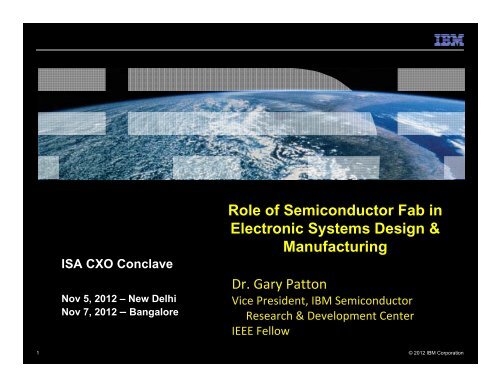
ISA CXO Conclave<br />
Nov 5, 2012 – New Delhi<br />
Nov 7, 2012 – Bangalore<br />
Role of Semiconductor Fab in<br />
Electronic Systems Design &<br />
Manufacturing<br />
Dr. Gary Patton<br />
Vice President, IBM Semiconductor<br />
Research & Development Center<br />
IEEE Fellow<br />
1<br />
© 2012 IBM Corporation
Chip Technology is Changing the World<br />
4 billion<br />
Power<br />
30 billion<br />
Number of RFID tags that will be embedded into Server/Network<br />
our world and across entire ecosystems<br />
Number<br />
by<br />
of<br />
2010<br />
connected devices in the world,<br />
constituting an “internet” of things<br />
2 billion<br />
Digital<br />
Camcorder<br />
Smart<br />
Tablet<br />
Video<br />
Game<br />
Devices<br />
1 trillion<br />
225,000 Data terabytes/month<br />
Processing<br />
Navigation<br />
System<br />
Estimated number of mobile<br />
Global mobile data traffic … more than 2x growth<br />
phone subscribers worldwide Digital TV over 2009, growing at 10x rate of voice traffic<br />
100 per day<br />
Number of texts the average<br />
Estimated number Phoneof people<br />
13- Speed to 17-year-old sends & receives<br />
on the internet by 2011<br />
Internet of Things<br />
ISA CXO Conclave –Nov 2012 2
Recent Smart phone / tablet phenomenon is fueling the<br />
mobile transformation<br />
Cell Phones Now Used More for Data<br />
Than for Calls 4<br />
“Instead of talking ….people are using<br />
it to …browse the web, listen to music,<br />
watch TV, play games, send e-mail and<br />
text messages.”<br />
Users expect mobile phones to<br />
replace GPS systems, MP3 players,<br />
and/or digital cameras by 2015. 5<br />
They want the ability to monitor and<br />
manage our home’s electricity use<br />
via mobile phones. 5<br />
Global Health Apps market to grow 24%<br />
Annually through 2014; Aged patients as well<br />
as patients suffering from chronic diseases<br />
prefer remote patient monitoring 2<br />
2<br />
1<br />
One of every three college students and employees surveyed<br />
Globally believes the Internet is a fundamental<br />
resource for the human race -- as important as air, water, food and shelter<br />
1. http://www.youtube.com/watch?v=lFZ0z5Fm-Ng&NR=1<br />
2. http://www.mobilehealthcaretoday.com/news/2011/09/<br />
3. Cisco connected world technology report 9/2011<br />
4. http://www.nytimes.com/2010/05/14/technology/personaltech/14talk.html?partner=rss&emc=rss<br />
5. “Opportunity Calling – The Future of Mobile Communications”, Oracle, 9/ 2010<br />
ISA CXO Conclave –Nov 2012 3<br />
3
Accelerating Advances in Technology<br />
Moore’s Law: doubling of chip<br />
integration every 12-18 months<br />
ISA CXO Conclave –Nov 2012 4
Exponential Technology Change<br />
If automobiles were like chips:<br />
1970 - 6 KM per Liter of gasoline<br />
1975 - 60 KM per Liter<br />
1980 - 600 KM per Liter<br />
1990 - 60,000 KM per Liter<br />
2000 - 6 Million KM per Liter<br />
ISA CXO Conclave –Nov 2012 5
Driving Force: Economics<br />
• Business Dynamics of the Semiconductor Industry in<br />
a 10 Year Cycle<br />
SCALING<br />
Exponential Growth in<br />
Investment in R&D and<br />
Manufacturing<br />
4x in 10 Years<br />
Exponential<br />
Improvement in<br />
Cost/Function:<br />
100x in 10 Years<br />
ELASTICITY<br />
Exponential Growth<br />
in Consumption of CEs<br />
400x in 10 Years<br />
Exponential Growth<br />
in Revenue:<br />
4x in 10 Years<br />
ISA CXO Conclave –Nov 2012 6
Advanced Technology for a wide range of applications<br />
MD’s selected semiconductor<br />
market segments (2011 total: $16.4B)<br />
Dollars (Billions)<br />
$18<br />
$16<br />
$14<br />
$12<br />
$10<br />
$8<br />
$6<br />
$4<br />
$2<br />
$0<br />
Auto<br />
A&D<br />
DP<br />
Industrial<br />
2009 2010 2011<br />
Wired<br />
Consumer<br />
Wireless<br />
These three<br />
segments make<br />
up 70% of MD’s<br />
OEM opportunity.<br />
Servers<br />
<strong>Smartphone</strong>s<br />
Routers &<br />
Switches<br />
WiFi, WiMAX<br />
Infrastructure<br />
Wireless<br />
Base Stations<br />
Storage<br />
TV Tuners,<br />
Video Processors<br />
Video<br />
Game Consoles<br />
Radio Network<br />
Controllers<br />
Optical<br />
Networks<br />
Communication<br />
Satellites<br />
7<br />
8 November 2012 IBM Confidential
End‐to‐end View of Semiconductor Application Market<br />
<strong>Smartphone</strong>s<br />
Game Consoles<br />
Internet of Things<br />
Smart<br />
surveillance<br />
Smart<br />
thermostats<br />
Smart<br />
lighting<br />
Radio<br />
Access<br />
Network<br />
Base<br />
station<br />
Backhaul<br />
(Copper,<br />
µwave<br />
or fibre)<br />
Radio<br />
Network<br />
Controller<br />
Wireless<br />
Core Network<br />
Mobile Operator<br />
Data Centers<br />
Internet/<br />
VPN<br />
Smart<br />
appliances<br />
Example applications<br />
Custom Processors<br />
Custom logic<br />
Specialty foundry<br />
Common Platform technology<br />
IBM systems & software<br />
ISA CXO Conclave –Nov 2012 8
<strong>Semiconductors</strong> in Servers and Supercomputers<br />
7 Oct 2009: Pres. Obama presented<br />
the 2008 National Medal of<br />
Technology and Innovation to IBM,<br />
the only company so honored, for<br />
the Blue Gene family of<br />
supercomputers…<br />
IBM Z<br />
Mainframe<br />
9<br />
ISA CXO Conclave –Nov 2012<br />
9
<strong>Semiconductors</strong> <strong>Inside</strong> a <strong>Smartphone</strong><br />
Power<br />
control<br />
PA<br />
PA<br />
Antenna tuner<br />
Switch<br />
PA<br />
PA<br />
Cellular front-end module (FEM)<br />
• Increasing bandwidth driven by new standards (4G/LTE)<br />
• Increasing complexity driving component integration and<br />
performance<br />
Key technologies:<br />
•RF CMOS, RF SOI, & SiGe<br />
Cellular transceivers /<br />
Analog baseband<br />
Wireless SoC<br />
transceiver<br />
(GPS, BT, Wi-Fi)<br />
TV tuner<br />
Power<br />
management<br />
Wi-Fi<br />
switch /<br />
LNA<br />
PA<br />
Digital baseband<br />
processors<br />
Applications<br />
processors<br />
Memory<br />
Wi-Fi FEM & TV Tuner<br />
• Becoming a standard on most<br />
phones to help offload data<br />
demand on base stations<br />
Key technologies:<br />
•RF CMOS, RF SOI, & SiGe<br />
Processor back-end module<br />
& Power Management<br />
Key technologies:<br />
•32/28 nm HKMG<br />
•HV CMOS<br />
*IBM MD Marketing estimates extrapolated from IBS<br />
12-11 NLT Foundry Mkt Trends data & IDC stats.<br />
ISA CXO Conclave –Nov 2012 10
<strong>Semiconductors</strong> <strong>Inside</strong> a <strong>Smartphone</strong><br />
32nm LP High‐k Metal Gate First Process<br />
Jointly developed with IBM<br />
Enabled to deliver twice the logic density of 45nm processes<br />
while maintaining low power, making it ideal for mobile applications<br />
Source: http://www.samsung.com/global/business/semiconductor/minisite/Exynos/products4quad.html<br />
11<br />
8 November 2012 IBM Confidential<br />
ISA CXO Conclave –Nov 2012 11
Classical Scaling and Reality<br />
• To maintain generational performance gains, supply voltage is not scaled<br />
ideally, leaving us with major power issues<br />
Voltage<br />
V / <br />
Ideal Scaling<br />
n+<br />
source<br />
tox/<br />
GATE<br />
WIRING<br />
n+<br />
drain<br />
W/<br />
L/<br />
xd/<br />
p substrate, doping *NA<br />
> 1<br />
Reality Scaling<br />
Voltage<br />
V / 1/2<br />
tox/<br />
n+<br />
source<br />
1/2<br />
GATE<br />
L/<br />
n+<br />
drain<br />
p substrate, doping *NA<br />
WIRING<br />
W/<br />
xd/<br />
gate<br />
source SiO 2 drain<br />
n+ channel n+<br />
p-type substrate<br />
Oxide down to only<br />
4 monolayers<br />
SCALING:<br />
Channel L L/<br />
Voltage: V/<br />
Oxide: tox /<br />
Wire width: W/<br />
Gate width: L/<br />
Diffusion: xd /<br />
Substrate: * NA<br />
On Current: <br />
RESULTS:<br />
2<br />
Higher Density: ~<br />
Higher Speed: ~<br />
2<br />
Power/ckt: ~1/<br />
Electric Field 1<br />
Power Density: ~1<br />
SCALING:<br />
Channel L L/<br />
1/2<br />
Voltage: V/<br />
1/2<br />
Oxide: tox /<br />
Wire width: W/<br />
Gate width: L/<br />
Diffusion: xd /<br />
Substrate: * NA<br />
On Current: 1/2<br />
<br />
RESULTS:<br />
2<br />
Higher Density: ~<br />
Higher Speed: ~<br />
Power/ckt: ~1/<br />
1/2<br />
Electric Field ~<br />
Power Density: ~<br />
Innovation, scaling, and power to drive performance !<br />
12
CMOS Scaling Realities: Pitch Degradation<br />
Significant innovation in performance‐enhancing elements required<br />
Node<br />
(nm)<br />
PC Pitch<br />
(m)<br />
180 0.7<br />
130 0.5<br />
90 0.35<br />
65 0.23<br />
45 0.18<br />
32 0.13<br />
22 0.1<br />
Relative Performance<br />
1.40<br />
1.35<br />
1.30<br />
1.25<br />
1.20<br />
1.15 Scaling In The Past…<br />
1.10<br />
1.05<br />
1.00<br />
0.95<br />
0.90<br />
0.85<br />
0.80<br />
Higher Capacitance<br />
Reduced Stress<br />
Scaling Now<br />
Channel Scaling<br />
High-k / Metal Gate<br />
Body Controlled Devices<br />
Reduced Gate Height<br />
Advanced BEOL Dielectric<br />
Higher Resistance<br />
Scaling<br />
Requirements<br />
ISA CXO Conclave –Nov 2012 13
Materials Innovations : Increased Complexity<br />
•Elements Employed in Silicon Technology<br />
Before 90’s<br />
Since the 90’s<br />
Beyond 2006<br />
ISA CXO Conclave –Nov 2012 14
Silicon Technology Roadmap<br />
• Major technology innovations “saturate” after about a decade<br />
• “Disruptive” Innovations will enable the next decades of progress<br />
Nanowire devices,<br />
3D multi-chip stacking &<br />
Photonics<br />
Performance, Density<br />
Planar CMOS<br />
Planar CMOS w/<br />
material & memory<br />
innovations<br />
3D Devices & 3D chip<br />
stacking, Adv. Power Mgt,<br />
Design-Tech Co-Optimization<br />
Emerald<br />
eDRAM<br />
Sapphire<br />
eDRAM<br />
Package<br />
Bipolar<br />
Bipolar<br />
Power<br />
Limit<br />
Gate<br />
Oxide<br />
Limit<br />
Planar<br />
Device<br />
Limit<br />
1980 1990 2000 2010 2020<br />
Atomic<br />
Dimension<br />
Limit<br />
ISA CXO Conclave –Nov 2012 15
Changing Innovation Requirements<br />
Atoms<br />
still don’t<br />
scale<br />
Traditional scaling is reaching its limits…but the<br />
economics of Moore’s Law are still holding…<br />
Yes, scaling<br />
can still drive<br />
down cost<br />
BUT<br />
It’s exponentially<br />
more costly<br />
to develop<br />
Continued advances mean changing the way we think about innovation<br />
Innovation<br />
Technical Innovation<br />
Business Model Innovation<br />
• Material & Process innovation must be able<br />
to counter the limits of traditional scaling<br />
• Long-term R&D focus/investment needed to<br />
drive this innovation and sustain roadmap<br />
• Design technology must be able to support &<br />
leverage materials and process innovation<br />
(Design-Technology Co-Optimization)<br />
• Collaborative R&D replaces independent<br />
R&D<br />
• Collaboration needs to include all functions<br />
(semiconductor manufacturers, equipment<br />
vendors, & material suppliers)<br />
• Shared investments / learning fosters<br />
breakthroughs beyond what would be<br />
possible for a single company / function<br />
ISA CXO Conclave –Nov 2012 16
Elements of an Open Collaborative Ecosystem:<br />
IBM Micro<strong>electronics</strong> Example<br />
• Mission: Provide world class semiconductor products<br />
through research, development, and manufacturing<br />
excellence to enable IBM systems and clients<br />
• Semiconductor Manufacturing Capabilities:<br />
– 200mm Manufacturing: 250nm+, 180nm, 130nm, 90nm nodes<br />
– 300mm Manufacturing: 90nm, 65nm, 45nm, 32nm nodes<br />
– Packaging: TSV 3D, flip chip, chip package interaction, Pb Free<br />
– Mask House: Capability for manufacturing nodes and advanced<br />
development<br />
– Yield / Factory Automation Software<br />
– Environmentally Friendly Manufacturing<br />
– Product Design / EDA capabilities<br />
Burlington, VT: 200mm Dev and Mfg<br />
Fishkill, NY: 300mm Dev and Mfg<br />
Bangalore, India: 200mm/300mm Dev<br />
• Research and Development Capabilities & Model:<br />
– Research and Development: 22nm, 14nm, 10nm =><br />
– World class technology research for materials, process,<br />
equipment, systems, and software<br />
– Collaboration model to create advanced semiconductor and<br />
packaging technologies with a range of partners<br />
• Process: Samsung, ST Micro, Global Foundries,…<br />
• Material: JSR, Rohm and Haas, BASF, etc<br />
• Equipment: Applied Materials, TEL, ASML, etc<br />
• Design / EDA: ARM, Cadence, Synopsis, Mentor Graphics, etc<br />
17 For Discussion Purposes only<br />
Albany NanoTech: 300mm R&D<br />
Watson Research Center (Yorktown,NY)<br />
Almaden Research Center (San Jose, CA)<br />
ISA CXO Conclave –Nov 2012 17
Government & University Partnerships to build Ecosystem:<br />
Albany Nanotech Research Center Example<br />
Litho Technology<br />
Leader<br />
#2 Equipment<br />
Supplier<br />
#1 Equipment Supplier<br />
Other JDA Partners<br />
Other Supplier Donations<br />
Fab Bld/Fit-Up / IMPLSE /<br />
CSR Tools<br />
Lam Research @ ANT<br />
IBM's Pre-T0 Partners<br />
CSR Tool Contributions<br />
(Phase 1, 2 and 3)<br />
Equipment Development Center (EDC)<br />
Other Equipment Supplier<br />
CSR Tool Contributions<br />
ISA CXO Conclave –Nov 2012 18
Innovation, Collaboration, & Government Partnership<br />
IBM Packaging Technology Corridor Example<br />
NY State Partnership<br />
C2MI Center<br />
CNSE CCIC Center<br />
East Fishkill PRDC<br />
IBM Research<br />
•Stand alone Bond and assembly line used to develop and<br />
launch products based upon JDA ecosystem technology<br />
•Focus on Product qualification & Process<br />
optimization for rapid manufacturing scale-up<br />
•Follow Silicon model & create world class packaging<br />
Research facility fostering collaboration between public and<br />
private entities<br />
•Current focus is W2W 3D integration<br />
•World class packaging interconnect and Bond & Assembly<br />
development facility in East Fishkill<br />
•Development of evolutionary and revolutionary<br />
packaging technology<br />
•World wide research across multiple labs, including Watson<br />
(NY), ZRL (Zurich) and TRL (Tokyo), ARL (Austin) and BRL<br />
(Brazil)<br />
•Fundamental research exploring new<br />
materials/process/paradigms<br />
ISA CXO Conclave –Nov 2012 19
IBM Semiconductor Research and Development<br />
Centers ‐ Around the World<br />
Almaden<br />
Malta (GF)<br />
Albany<br />
Fishkill<br />
Yorktown<br />
Bromont<br />
Burlington<br />
Zurich<br />
Crolles, France<br />
(STM)<br />
Korea<br />
(SEC)<br />
Bangalore<br />
IBM Research<br />
IBM SRDC<br />
IBM Teams based at Partner Locations<br />
ISA CXO Conclave –Nov 2012 20
Semiconductor Research & Development Center (SRDC)<br />
Bangalore, India<br />
TCAD Development<br />
Ab-initio Modeling<br />
Compact Modeling<br />
Computational<br />
Lithography<br />
Process & Device Characterization<br />
Process Window Analysis<br />
Fail Rate<br />
Electrical Data vs<br />
Design Electrical / Process Data<br />
Metrology Design / Data Process<br />
Metrology Data<br />
ISA CXO Conclave –Nov 2012<br />
21
Silicon through Systems –India Technology &<br />
Hardware Development<br />
Systems Engineering<br />
• Post Silicon Validation<br />
• Validation Tools Development<br />
• Memory, Processor, System Characterization<br />
• Processor & System Performance Modeling<br />
Core 0<br />
MC<br />
IOs<br />
L2<br />
MCU<br />
CoP<br />
L2<br />
MC<br />
IOs<br />
Core 1<br />
L3B<br />
L3_0<br />
L3_0<br />
L3_0 Controller<br />
L3_1 Controller<br />
L3B<br />
L3_1<br />
L3_1<br />
Core 2<br />
GX<br />
IOs<br />
L2<br />
CoP<br />
GX<br />
L2<br />
GX<br />
IOs<br />
Core 3<br />
Processors and System ASICs<br />
Logic Design and Verification<br />
• Server ASICs<br />
• Server Processors<br />
• Pervasive Design & Verification<br />
Physical Design and Layout<br />
• POWER & System Z processors<br />
Custom Logic – ASICs & IP<br />
• Delivery - ASIC Design Centre<br />
• IP - High Speed Serial Links & Analog Cores, Memory Compilers<br />
• Enablement - Test Manufacturing Data, Foundry / ASIC Enablement & Library Development<br />
EDA<br />
• Physical Design & Timing: Place & Route Flows, Layout Automation, Library charc., Timing tools & methodology<br />
• Front End & Verification: DFT methodology, Functional & Formal Verification debug tools<br />
• Enablement & Support: System Test, Data Management, Customer Support<br />
<strong>Semiconductors</strong><br />
200mm Enablement<br />
* Compact Modeling<br />
* Enablement<br />
Lithography<br />
* Pattern Correction<br />
* OPC Modeling<br />
Nanotechnology<br />
* MultiScale Modelling<br />
* TCAD Development<br />
eDRAM<br />
* eDRAM Design<br />
* Characterization<br />
Technology Software Engg<br />
* CAYCE<br />
* MD Parts<br />
Technical Breadth & Delivery across the System Hardware stack<br />
ISA CXO Conclave –Nov 2012 22
From Atoms to Supercomputers<br />
End-to-End Materials and Technology<br />
Innovation and Enablement<br />
for Semiconductor Chips and<br />
Computing Systems<br />
Servers and Supercomputers<br />
Atoms and<br />
Molecules :<br />
Materials<br />
Innovation<br />
NanoDevice<br />
technology<br />
Electronic<br />
Design and<br />
Processor<br />
Enablement<br />
Power 7+ Process Chip<br />
– 567mm2 32nm SOI eDRAM technology<br />
– Eight processor cores<br />
– 80MB on chip eDRAM shared L3<br />
– Equivalent function of 5.4B transistors<br />
ISA CXO Conclave –Nov 2012 due to eDRAM efficiency
Growing an Ecosystem<br />
Key Elements<br />
Market expertise<br />
SoC reference designs<br />
Turn‐key design services<br />
Design services –front end,<br />
back end, test, packaging<br />
RTL to GDSII reference flows<br />
Industry standard design<br />
tools<br />
Segment based IP –USB,<br />
HDMI, LPDDR, SATA….<br />
Foundation IP – libraries,<br />
memories, IO, PLLs…<br />
Foundry services –masks,<br />
MPWs, packaging, test<br />
Industry compatible PDK<br />
Competitive base technology<br />
India<br />
Product<br />
Development<br />
India<br />
Design<br />
services<br />
Design<br />
flows<br />
IP<br />
enablement<br />
Foundry<br />
technology<br />
India fab services<br />
Leverage<br />
Grow internal system design,<br />
architecture, product<br />
marketing, & field applications.<br />
3’rd party SoC ecosystem –<br />
ARM processors, Synopsys<br />
DesignWare<br />
Existing Indian design services<br />
infrastructure<br />
3’rd party EDA tools, reference<br />
flows, & sign-off solutions<br />
3’rd party IP, already designed<br />
& verified in existing industry<br />
technology<br />
Existing IBM foundry<br />
manufacturing ecosystem<br />
IBM technology &<br />
manufacturing expertise<br />
24 ISA CXO Conclave –Nov 2012 IBM Confidential 24
Semiconductor Industry Enablement Offerings<br />
For an end‐to‐end Semiconductor Modules Manufacturing Industry base<br />
• Ongoing access to a leadership CMOS wafer process technology roadmap<br />
– Including design enablement<br />
– Multiyear technology delivery commitment from IBM to Client<br />
• Semiconductor Manufacturing methodology / controls<br />
• Semiconductor Yield methodology<br />
• Technology Ramp/Training<br />
– Round robin wafer exchange<br />
– Failure analysis technology/methodology<br />
– Ongoing rotational training assignment in East Fishkill<br />
• Technology, manufacturing, logistics, controls, organizational<br />
– Product level transfer/yield compare<br />
• Dependent on initial product identified by Partner<br />
• IT Infrastructure<br />
– Servers, middleware, data warehouse<br />
– Manufacturing Execution system<br />
– Manufacturing yield, test, control software<br />
• Design IP<br />
• Design Tools<br />
• Wafer Bumping Technology<br />
• Wafer & Module Test Methodology<br />
• Packaging Technology<br />
Foundry<br />
Design House<br />
Packaging Assembly<br />
& Testing Company<br />
ISA CXO Conclave –Nov 2012 25
What will a Semiconductor Manufacturing Ecosystem<br />
do for India?<br />
– Address Import/Export Supply Gap<br />
• Domestic electronic products demand is projected to be $400B in 2020.<br />
• Domestic production expected to cover only $100B.<br />
• Import/Export Gap: $300B! (projected to exceeds India’s oil import bill<br />
in 2020!!)<br />
– Address National and information security<br />
– Create Sourcing stability and self‐reliance<br />
– Launch a Platform for scientific innovation and R&D based industries –<br />
Build on India’s current talent pool and design<br />
– Job creation: MANYjobs created beyond direct fab operations<br />
– Possible focus area : Set top boxes, Smart Phones, Tablets, Smart Meters,<br />
micro‐ATMs, Smart Cards, Sensors<br />
ISA CXO Conclave –Nov 2012 26
Summary<br />
• CMOS scaling will continue, requiring innovation and<br />
optimization in lithography, materials and device<br />
structures<br />
• New “disruptive” technologies coupled with CMOS<br />
scaling will enable performance growth to exascale<br />
• Solutions designed to deliver maximum value to the<br />
customer<br />
• Fab can be a catalyst for broad Electronic Systems Design<br />
and Manufacturing ecosystem<br />
27<br />
ISA CXO Conclave –Nov 2012 27
Thank You<br />
ISA CXO Conclave –Nov 2012 28