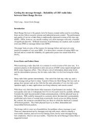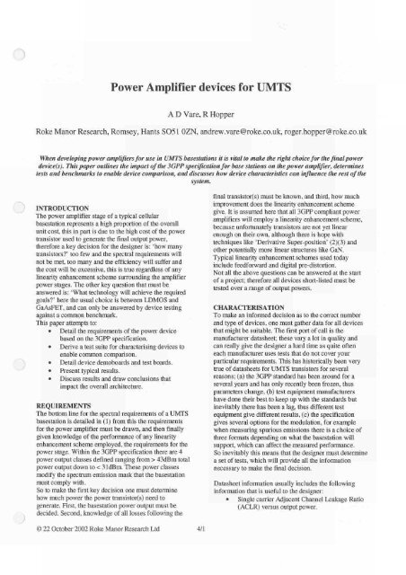
Power Amplifier devices for UMTS
Power Amplifier devices for UMTS
Power Amplifier devices for UMTS

Create successful ePaper yourself
Turn your PDF publications into a flip-book with our unique Google optimized e-Paper software.
<strong>Power</strong> <strong>Amplifier</strong> <strong>devices</strong> <strong>for</strong> <strong>UMTS</strong><br />
A D Vare, R Hopper<br />
Roke Manor Research, Romsey, Hants S051 OZN, andrew.vare@roke.co.uk , roger.hopper@roke.co.uk<br />
When developing power amplifiers <strong>for</strong> use in <strong>UMTS</strong> basestations it is vital to make the right choice <strong>for</strong> the final power<br />
device(s). This paper outlines the impact of the 3GPP specification <strong>for</strong> base stations on the power amplifier, determines<br />
tests and benchmarks to enable device comparison, and discusses how device characteristics can influence the rest of the<br />
system.<br />
INTRODUCTION<br />
The power amplifier stage of a typical cellular<br />
basestation represents a high proportion of the overall<br />
unit cost, this in part is due to the high cost of the power<br />
transistor used to generate the final output power,<br />
there<strong>for</strong>e a key decision <strong>for</strong> the designer is: `how many<br />
transistors?' too few and the spectral requi rements will<br />
not be met, too many and the efficiency will suffer and<br />
the cost will be excessive, this is true regardless of any<br />
linearity enhancement scheme surrounding the amplifier<br />
power stages. The other key question that must be<br />
answered is: `What technology will achieve the required<br />
goals?' here the usual choice is between LDMOS and<br />
GaAsFET, and can only be answered by device testing<br />
against a common benchmark.<br />
This paper attempts to:<br />
• Detail the requirements of the power device<br />
based on the 3GPP specification.<br />
• Derive a test suite <strong>for</strong> characterising <strong>devices</strong> to<br />
enable common comparison.<br />
• Detail device demoboards and test boards.<br />
• Present typical results.<br />
• Discuss results and draw conclusions that<br />
impact the overall architecture.<br />
REQUIREMENTS<br />
The bottom line <strong>for</strong> the spectral requirements of a <strong>UMTS</strong><br />
basestation is detailed in (1) from this the requirements<br />
<strong>for</strong> the power amplifier must be drawn, and then finally<br />
given knowledge of the per<strong>for</strong>mance of any linearity<br />
enhancement scheme employed, the requirements <strong>for</strong> the<br />
power stage. Within the 3GPP specification there are 4<br />
power output classes defined ranging from > 43dBm total<br />
power output down to < 31dBm. These power classes<br />
modify the spectrum emission mask that the basestation<br />
must comply with.<br />
So to make the first key decision one must determine<br />
how much power the power transistor(s) need to<br />
generate. First, the basestation power output must be<br />
decided. Second, knowledge of all losses following the<br />
final transistor(s) must be known, and third, how much<br />
improvement does the linearity enhancement scheme<br />
give. It is assumed here that all 3GPP compliant power<br />
amplifiers will employ a linearity enhancement scheme,<br />
because un<strong>for</strong>tunately transistors are not yet linear<br />
enough on their own, although there is hope with<br />
techniques like `Derivative Super-position' (2)(3) and<br />
other potentially more linear structures like GaN.<br />
Typical linearity enhancement schemes used today<br />
include feed<strong>for</strong>ward and digital pre-distortion.<br />
Not all the above questions can be answered at the start<br />
of a project; there<strong>for</strong>e all <strong>devices</strong> short-listed must be<br />
tested over a range of output powers.<br />
CHARACTERISATION<br />
To make an in<strong>for</strong>med decision as to the correct number<br />
and type of <strong>devices</strong>, one must gather data <strong>for</strong> all <strong>devices</strong><br />
that might be suitable. The first port of call is the<br />
manufacturer datasheet; these vary a lot in quality and<br />
can really give the designer a hard time as quite often<br />
each manufacturer uses tests that do not cover your<br />
particular requirements. This has historically been very<br />
true of datasheets <strong>for</strong> <strong>UMTS</strong> transistors <strong>for</strong> several<br />
reasons; (a) the 3GPP standard has been around <strong>for</strong> a<br />
several years and has only recently been frozen, thus<br />
parameters change, (b) test equipment manufacturers<br />
have done their best to keep up with the standards but<br />
inevitably there has been a lag, thus different test<br />
equipment give different results, (c) the specification<br />
gives several options <strong>for</strong> the modulation, <strong>for</strong> example<br />
when measuring spurious emissions there is a choice of<br />
three <strong>for</strong>mats depending on what the basestation will<br />
support, which can affect the measured per<strong>for</strong>mance.<br />
So inevitably this means that the designer must determine<br />
a set of tests, which will provide all the in<strong>for</strong>mation<br />
necessary to make the final decision.<br />
Datasheet in<strong>for</strong>mation usually includes the following<br />
in<strong>for</strong>mation that is useful to the designer:<br />
• Single carrier Adjacent Channel Leakage Ratio<br />
(ACLR) versus output power.<br />
© 22 October 2002 Roke Manor Research Ltd 4/1
• Two carrier ACLR and 3'd Order<br />
Intel-modulation Distortion (IMD) versus output<br />
power.<br />
• Optimised source and load impedances (useful<br />
<strong>for</strong> the test circuit).<br />
However quite often the modulation used <strong>for</strong> the<br />
measurements is not fully described in terms of statistics,<br />
or varies between manufacturers, or worse still, not even<br />
stated, necessitating re-measurement to a common<br />
standard. In some cases the designer may have a special<br />
modulation employing clipping algorithms, which would<br />
have to be used.<br />
In addition to the above data, the designer would also<br />
want to characterise the following parameters using a test<br />
circuit or demoboard:<br />
• S parameters over frequency.<br />
• Gain and phase compression.<br />
• 2 carrier CW IMD products, 3 `d , 5 `h , and 7`h at<br />
least.<br />
• Sensitivity to variation in Idq.<br />
To make these measurements repeatable and to remove<br />
the drudgery it is essential to automate the process as<br />
much as possible. At RMRL a suite of programs have<br />
been written using Agilent VEE, which has enabled a<br />
database of over 300MB to be generated <strong>for</strong> a broad<br />
spectrum of parts.<br />
As well as spectral, (1) also contains other requirements<br />
that relate to the wanted signal modulation quality,<br />
namely Error Vector Magnitude (EVM), and Peak Code<br />
Domain Error (PCDE), both defined in section 6.7 of (1).<br />
These requirements are very important as they relate to<br />
the overall bit error rate <strong>for</strong> the base station transmitter.<br />
The power amplifier will contribute to the overall figures<br />
of EVM and PCDE, but measurements have shown that<br />
if the power amplifier meets the spectral requirements<br />
then the linearity is sufficiently good such that the<br />
contribution to signal modulation quality will be<br />
negligible. There<strong>for</strong>e swept measurements of EVM and<br />
PCDE versus power output do not necessarily need to be<br />
included in the test suite.<br />
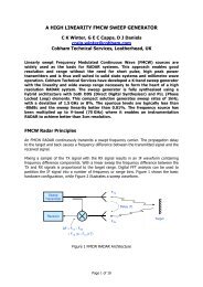
W-CDMA TEST SIGNAL<br />
Within the 3GPP specification, there are options as to the<br />
modulation <strong>for</strong>mat, these are referred to as `test models'.<br />
There are basically 4 different test models, each used <strong>for</strong><br />
specific tests, in the case of ACLR and spurious<br />
emissions the relevant test model is Test Model 1,<br />
defined in (1) 6.1.1.1. However within this test model<br />
there are 3 options; 16, 32 and 64 DPCH (Dedicated<br />
Physical CHannel) or `users', this results in a spread<br />
spectrum signal which exhibits a high peak to mean ratio<br />
dependant on the option chosen. Figure 1 plots the<br />
theoretical Complementary Cumulative Density Function<br />
(CCDF) <strong>for</strong> each option. It shows that there is about 1dB<br />
difference in absolute peak power between each option.<br />
This can affect the test results, there<strong>for</strong>e <strong>for</strong> repeatability<br />
reasons, one option should be standardised on. At RMRL<br />
the 64 DPCH has been decided on as this stresses the<br />
transistor to the maximum.<br />
In most base stations a clipping algorithm is employed in<br />
DSP at the baseband stage to reduce the maximum peak<br />
of the signal in order to reduce the stress on the power<br />
amplifier, allowing it to provide more power and hence<br />
better efficiency. However when choosing <strong>devices</strong> it is<br />
better to consider testing using an unclipped wave<strong>for</strong>m<br />
since this represents a worse case scenario. Results<br />
should only improve with clipping. It adds a safety<br />
margin <strong>for</strong> the designer, and provides protection from<br />
changes to the actual clipping algorithm.<br />
Figure 1: Test Model 1/64 CCDF cuove<br />
TEST BENCH<br />
For testing high power <strong>devices</strong> a special test setup is<br />
required comprising:<br />
• A high power dc supply.<br />
• 2 x W-CDMA capable signal generators, e.g.<br />
Agilent ESG or Rohde and Schwarz SMIQ.<br />
• 2 x High power class A driver amplifiers.<br />
• Isolators.<br />
• High power directional couplers.<br />
• High power attenuators.<br />
• 2 x power meters.<br />
• High dynamic range spectrum analyser with rms<br />
detector and ACLR measuring capability e.g.<br />
Rohde and Schwarz FSIQ.<br />
A typical test setup is given in Figure 2 below:<br />
Note that the two tone signal is generated by combining<br />
at high power, and note the use of isolators, both<br />
measures ensure that source IMD is negligible. The<br />
whole test set-up must be carefully calibrated <strong>for</strong> loss<br />
with a network analyser to ensure accurate measurements<br />
since a loss of 0.2dB already represents 1W in 20W.<br />
Note also that (1) 6.1.1.6.3 states that each modulated<br />
carrier shall have a different scrambling code,<br />
incremented from 0 starting with the lowest carrier<br />
frequency, there shall also be 1/5 time slot offset between<br />
their frame structures. This again will make a minor<br />
© 22 October 2002 Roke Manor Research Ltd 4/2
1 ACLR<br />
-i^<br />
0<br />
Agilent<br />
ESG<br />
45dBm<br />
Driver<br />
Isolator<br />
Isolator<br />
20dB<br />
Coupler<br />
30dB<br />
Coupler<br />
40dB<br />
Attenuator<br />
<strong>Power</strong> Meter<br />
E4418B<br />
Agilent<br />
ESG<br />
45dBm<br />
Driver<br />
Isolator<br />
0<br />
Figure 2: Typical IMD/ACLR test setup<br />
difference to the composite peak to mean ratio and<br />
should be included as part of the test setup.<br />
BENCHMARK TEST<br />
If certain assumptions can be made about system<br />
per<strong>for</strong>mance it is possible to generate a `benchmark' test<br />
that allows easy comparison of <strong>devices</strong>. The fast step is<br />
to extract the most demanding requirement from (1), the<br />
situation changes depending on the number of carriers<br />
the amplifier is required to pass. With one carrier there<br />
are no discrete IlViDs to worry about and the most<br />
stringent spectral requirement is the out of band emission<br />
found in (1) 6.5.2.1.2, this is illustrated in Figure 3, also<br />
shown are the less stringent requirements of ACLR. It<br />
can be seen that the requirement level in dBm is<br />
-28.2dBm/30kHz, given a 43dBm carrier this translates<br />
to -50.2dBc.<br />
30 -- - _ __ _ ...<br />
20<br />
10<br />
0<br />
4<br />
43dBrr carnet<br />
Spectrum<br />
Analyser<br />
FS IQ<br />
requirement is the category B Spurious emission mask<br />
found in section 6.5.3.4.2. This requirement is<br />
considerably tougher than ACLR or out of band emission<br />
<strong>for</strong> one or more carriers. Figure 4 below shows a<br />
composite plot of the spectral requirements assuming a 2<br />
carrier transmitter at the bottom of the frequency band<br />
2110 to 2170MHz. The carrier spacing <strong>for</strong> the 2 carrier<br />
signal is 15MHz, this means that the lower third order<br />
IMD product will fall at 2097.5MHz and will be required<br />
to be below the -45dBm/30kHz category B mask limit.<br />
30<br />
20<br />
i 10<br />
1 o<br />
^<br />
> - 10 -<br />
Ex<br />
QlgOry B<br />
43d8m career<br />
Band 2110 to 2170NHz<br />
-20 t e,n^ I / ,k<br />
iml<br />
-40<br />
-50<br />
2080 2100 2110 2120 2130 2140 2150<br />
Frequency (MHz)<br />
snya<br />
E -<br />
E<br />
10 RCL A<br />
Gleamy B<br />
(( )<br />
i.<br />
_.. -1-<br />
Band 21101o 2170M-lz<br />
5^-<br />
. -20<br />
M1<br />
l , '-<br />
musk<br />
40<br />
{I--L<br />
50<br />
2090 2100 2110 2120 2130 2140 2150<br />
Frequency (MHz)<br />
Figure 4: Two carrier <strong>UMTS</strong> spectrum requirements<br />
Translated to dB relative to a 43dBm carrier results in a<br />
level of -67dBc. In order to generate a benchmark IMD<br />
level <strong>for</strong> the power stage, the losses at 2097.5MHz<br />
relative to the wanted band e.g. duplexer filter, plus the<br />
linearity scheme enhancement must be subtracted from<br />
the -67dBc figure. In practise a general figure of about<br />
-35dBc results.<br />
Figure 3: Single Carrier <strong>UMTS</strong> spectrum requirements<br />
However, most amplifiers are designed to handle at least<br />
two carriers and in this case the most stringent<br />
© 22 October 2002 Roke Manor Research Ltd<br />
4/3
TWO CARRIER BENCHMARK:<br />
Total 3GPP requirement = -67dBc<br />
Linearity improvement scheme = 20dB<br />
Duplexer out of band loss*= 10dB<br />
Margin =<br />
2dB<br />
<strong>Power</strong> stage IMD level = -35dBc<br />
only a temporary solution as the gate bias circuit should<br />
really be thermally connected to the power transistor in<br />
order <strong>for</strong> the transistor Idq to be correctly thermally<br />
compensated. Note also that the power transistor is not<br />
soldered, this is only acceptable <strong>for</strong> a test board, where<br />
<strong>devices</strong> are to be compared, soldering makes this hard<br />
work.<br />
* K&L WSD-00189 <strong>UMTS</strong> duplexer<br />
The linearisation improvement figure of 20dB suggests<br />
that a feed<strong>for</strong>ward system is requi red to produce a<br />
compliant multi-carrier amplifier.<br />
DEMOBOARDS AND TEST BOARDS<br />
The quickest route to characterising a device is to obtain<br />
an application demoboard from the transistor<br />
manufacturer. The demoboards are designed to be as<br />
flexible as possible and adjustable tuning elements are<br />
often included <strong>for</strong> optimisation. The user can there<strong>for</strong>e<br />
optimise the demoboard to some degree <strong>for</strong> their<br />
particular application. However it is necessary at some<br />
point to make your own board customised to your<br />
application and manufacturing philosophy.<br />
Sometimes the delivery of a demoboard is either outside<br />
of your timescales or simply not available, in this case it<br />
is necessary to make your own board from the outset.<br />
Designing your own test board <strong>for</strong> a high power<br />
transistor is at lust a rather slow process as there are<br />
significantly more steps involved compared to say a<br />
small signal device, in particular with regard to the<br />
mechanical and heatsinldng arrangements. The typical<br />
tasks involved include the following:<br />
• If gerber files <strong>for</strong> a test board can be obtained<br />
from the manufacturer, use them!<br />
• No gerber files, then hopefully obtain the<br />
manufacturer declared optimum source and load<br />
impedances, decide what they mean and use<br />
them as a starting point <strong>for</strong> matching circuits.<br />
• Design the test board including bias networks.<br />
• Design the heatsink and / or baseplate.<br />
• Have all parts manufactured.<br />
• Build the pcbs and assemble the completed test<br />
board onto the heatsink.<br />
• Test the test board, and tune up if necessary.<br />
• Compare the results against the datasheet.<br />
Figure 5 is an example of a test board <strong>for</strong> a Motorola<br />
MRF 21125 based on manufacturer supplied data, it is<br />
part of a family of test boards all designed around the<br />
same heat sinking and biasing arrangements in order to<br />
speed up development of a test board <strong>for</strong> a new device. It<br />
can be seen that the gate and drain circuitry can be<br />
rapidly removed and replaced in order to experiment with<br />
different matching circuits. The gate bias circuit is also<br />
on a separate board <strong>for</strong> the same reason, however this is<br />
Figure 5: Typical power device testboard<br />
TYPICAL CHARACTERISATION RESULTS<br />
Figure 6 below shows small signal gain curves over a<br />
frequency sweep of 500MHz centered on 2140MHz. It<br />
compares a typical demoboard against another transistor<br />
of the same family optimised <strong>for</strong> flat gain. Flat gain is<br />
important <strong>for</strong> manufacture repeatability as a `peaked'<br />
response is more sensitive to component tolerances.<br />
18<br />
16<br />
4<br />
S 12<br />
cr) 10<br />
CI)<br />
I<br />
6<br />
2<br />
0<br />
IuMTB<br />
Band<br />
^ ^'<br />
nn<br />
1 ? nnr...<br />
-Typical demoboard<br />
-Bandwidth optimised<br />
design<br />
1.89 2.14 2.39<br />
Frequency (MHz)<br />
Figure 6: Small Signal Gain<br />
Flat gain (and phase) over frequency is also a very<br />
important characteristic when linearisation is employed.<br />
In the case of a feed<strong>for</strong>ward system the amplitude (and<br />
© 22 October 2002 Roke Manor Research Ltd 4/4
phase) ripple limits the amount of improvement that can<br />
be obtained over a given bandwidth.<br />
The amount of improvement or cancellation is given the<br />
equation below found in (4):<br />
A<br />
S:=10 .1og[ 10 10/ +1-410 01.cos(1, ),<br />
Where A is the amplitude ripple in dB, and 4 is the phase<br />
ripple, both over the bandwidth of interest. Taking the<br />
two <strong>devices</strong> above over a bandwidth of 15MHz, and<br />
60MHz, and the following cancellation figures result<br />
assuming the phase ripple <strong>for</strong> both <strong>devices</strong> were equal to<br />
zero:<br />
Device<br />
Carrier spacing Standard<br />
demoboard<br />
Optimised<br />
device<br />
15MHz -33.70dB -64.80dB<br />
60MHz -25.76dB -38.48dB<br />
Compared to the 2 carrier benchmark described earlier<br />
where 20dB is required from the lineariser, the standard<br />
demoboard would cause severe limitations as carrier<br />
spacing is increased as on its own would consume nearly<br />
all the budget just due to gain ripple. The figures will be<br />
worse if phase ripple were included. The output stage<br />
considered here will be only one part of the complete<br />
amplifier line-up and the way the S21 of all the <strong>devices</strong><br />
interact would have to be carefully considered.<br />
Figure 7 below shows a typical plot of power gain and<br />
phase versus input power level. The amplifier<br />
compression at the higher power levels can be clearly<br />
seen.<br />
19<br />
18<br />
17<br />
16<br />
12<br />
11<br />
I I I I J<br />
-40<br />
-Ma g (dB) - -45<br />
--Phase (deg) - -50<br />
-55<br />
-60<br />
-s5<br />
-70<br />
-75<br />
-80<br />
gain peaks are a <strong>for</strong>m of build-in pre-distortion giving a<br />
little gain expansion. The gain response can also interact<br />
with the phase curve to give the same result. If the<br />
transistor manufacturer had better control of the device<br />
transconductance curve then maybe we might see<br />
improved transistors and the goal of a class AB amplifier<br />
without an external lineariser might be achievable.<br />
It is still useful to plot the gain and phase of a transistor<br />
versus power level, but is not ideal <strong>for</strong> optimising<br />
linearity, it is far better to adjust Idq whilst observing<br />
IMD directly.<br />
As mentioned above Idq has a strong effect on the<br />
linearity of a device, this can be easily observed in Figure<br />
8 which shows 3'd order IMD levels versus average<br />
power output from a typical LDMOS device as Idq is<br />
varied. For this particular device the optimum Idq under<br />
CW excitation is about 1.30A. Similar plots could be<br />
drawn <strong>for</strong> 5th and 7th order products, however generally<br />
3rd order is dominant and so optimising Idq <strong>for</strong> this order<br />
is normally adequate. Note <strong>for</strong> this device the dip in IMD<br />
or `sweet spot' at 40dBm output level at an Idq of 1.3A.<br />
Characterisation using CW is very useful <strong>for</strong> carrying out<br />
an initial comparison of <strong>devices</strong> and optimisation,<br />
however the per<strong>for</strong>mance will change considerably under<br />
W-CDMA excitation due to the high peak to mean ratio<br />
and spread spectrum characteristics of the signal. Figure<br />
9 shows ACLR versus output power <strong>for</strong> the same device<br />
as shown in Figure 8. By comparison the following<br />
points can be drawn:<br />
• At high power s45dBm, the IMD/ACLR levels<br />
are similar and the amplifier is driven well into<br />
compression by the peaks of the signal.<br />
• With W-CDMA the `sweet spots' have<br />
disappeared.<br />
• Significant `memory effect' or ACLR imbalance<br />
is evidence with W-CDMA as power is backed<br />
off.<br />
• At high Idq where the device is getting closer to<br />
class A bias, the back off curve with W-CDMA<br />
retains the shape seen with CW, albeit at an<br />
overall lower level.<br />
• The optimum Idq setting <strong>for</strong> single car rier W-<br />
CDMA has increased to =1.6A.<br />
10<br />
-85<br />
9<br />
-so<br />
10 15 20 25 30 35 40 45<br />
Input power (dBm)<br />
Figure 7: CW power sweep<br />
The absolute gain and shape of the compression curve is<br />
related to the quiescent current (Idq) of the transistor<br />
which <strong>for</strong> a class AB stage will be in the region of 10%<br />
of Id max. It is important to set the optimum Idq <strong>for</strong> best<br />
efficiency and linearity. Linearity is strongly affected by<br />
Idq due to the gain peaks as the device approaches<br />
saturation, these cause so called IMD `sweet spots', the<br />
© 22 October 2002 Roke Manor Research Ltd 4/5
0<br />
-10<br />
-60<br />
-+3rd imd 0.70A<br />
-+3rd imd 1.OOA<br />
-+3rd imd 1.30A<br />
-+3rd imd 1.60A<br />
+3rd imd 1.90A<br />
- -Efficiency 0.7A<br />
Efficiency 1.3A<br />
_ Efficiency 1.9A<br />
lr<br />
3rd imd<br />
- - --3rd imd 0.70A<br />
1.00A<br />
-3rd imd 1.30A<br />
- - - - -3rd imd 1.60A<br />
-3rd imd 1.9A<br />
-Efficiency 1.0A<br />
-Efficiency 1.6A<br />
AdMal<br />
80<br />
0 80<br />
-+3rd imd 0.70A<br />
3rd imd 0.70A<br />
-+3rd imd 1.OOA<br />
3rd imd 1.OOA<br />
70<br />
+3rd imd 1.30A<br />
-3rd imd 1.30A - 70<br />
-10<br />
- +3rd imd 1.60A<br />
3rd imd 1.60A<br />
-+3rd imd 1.90A<br />
-3rd imd 1.9A<br />
60<br />
u -20 - -Efficiency 0.7A - - -Efficiency 1.0A - 60<br />
Efficiency 1.3A - - -Efficiency 1.6A -<br />
Efficiency 1.9A<br />
50 Z.<br />
50 g'<br />
U<br />
-30<br />
T..<br />
u<br />
40 40 `2v m<br />
-40<br />
30 W 30 W<br />
0<br />
-50<br />
20<br />
20<br />
-70<br />
10 -60<br />
10<br />
-80<br />
0 -70<br />
20 25 30 35 40 45 50<br />
20<br />
25<br />
30 35 40<br />
0<br />
45<br />
Average output power (dBm)<br />
Average output power (dBm)<br />
Figure 8: CW IMD versus Idq<br />
Figure 10: IMD with 2 x W-CDMA source<br />
-10<br />
-20<br />
+ACLR 0.70A - --ACLR 0.70A<br />
+ACLR 1.OOA ACLR 1.OOA<br />
+ACLR 1.30A -ACLR 1.30A<br />
+ACLR 1.60A ACLR 1.60A<br />
+ACLR 1.90A -ACLR 1.9A<br />
Efficiency 0.7A -Efficiency 1.0A<br />
Efficiency 1.3A -Efficiency 1.6A<br />
Efficiency 1.9A<br />
80<br />
70<br />
60<br />
Here we see:<br />
• `Sweet spots' very sensitive to Idq.<br />
• Large memory effect.<br />
• Optimum Idq now = 1.9A (at 2 carrier<br />
benchmark -35dBc).<br />
-70<br />
-80 -<br />
20<br />
+ACLR 0.70A --ACLR 0.70A<br />
-10 -<br />
---+ACLR 1.OOA ACLR 1.OOA<br />
+ACLR 1.30A -ACLR 1.30A<br />
-+ACLR 1.60A ACLR 1.60A<br />
-+ACLR 1.90A -ACLR 1.9A<br />
- -Efficiency 0.7A - - -Efficiency 1.0A<br />
Efficiency 1.3A - - -Efficiency 1.6A<br />
Efficiency 1.9A<br />
80<br />
70<br />
60<br />
Figure 9: ACLR with 1 x W-CDMA source<br />
ACLR with a spread signal is really a composite of 3 `d ,<br />
5th 7`h etc orders of IMD products added together over<br />
the complete range of baseband frequencies, or like a<br />
closely spaced multi-tone CW signal, thus it is no<br />
surprise that the plots seen in Figure 8 and Figure 9 are<br />
so different.<br />
Now consider the case of a two can•ier W-CDMA signal<br />
applied to the same amplifier, see Figure 10 and Figure<br />
11 below.<br />
In Figure 10 the plot of 3rd order IMD it can be seen that<br />
the `sweet spots' have reappeared, but there is significant<br />
`memory effect' with more than 10dB IMD imbalance<br />
noted at some power levels. This points to poor design of<br />
this particular demoboard supplied as is from the<br />
manufacturer.<br />
Figure 11: ACLR (lower carrier) with 2 x W-CDMA source<br />
Figure 11 shows the ACLR plot <strong>for</strong> the same 2 carrier<br />
W-CDMA input signal, but just considering the lower of<br />
the two carriers, in practise the other carrier will exhibit<br />
essentially the same set of curves. The plots are<br />
significantly different to the single carrier case shown in<br />
Figure 9, however with two carriers the absolute peak to<br />
mean ratio will have been modified to perhaps 12dB so<br />
this is no surprise.<br />
Here we conclude:<br />
• ACLR with two carriers is significantly lower in<br />
level compared to 3rd order IMD (5dB or more<br />
at high power), there<strong>for</strong>e less important.<br />
Normally improving the 3rd order IMD to meet<br />
specification will automatically ensure ACLR is<br />
acceptable.<br />
• Optimum Idq is again = 1.9A.<br />
© 22 October 2002 Roke Manor Research Ltd 4/6
IMPACT OF MEMORY EFFECT<br />
As observed Figure 10, this particular demoboard<br />
exhibited quite different memory effects under 2 carrier<br />
CW conditions compared to 2 carrier W-CDMA<br />
conditions: in the CW case hardly any memory was<br />
observed and in the W-CDMA case up to a very poor<br />
10dB was noticed.<br />
If 10dB IMD imbalance exists at the benchmark level<br />
then the implications are that if the higher of the two<br />
IMDs is enhanced by the memory effect whilst the other<br />
is cancelled then the amplifier is not providing the power<br />
it could if there were no memory effect. This means that<br />
with a feed<strong>for</strong>ward amplifier either the correction has to<br />
work harder or the amplifier has to be backed off more<br />
with the hit on efficiency. Neither case is desirable.<br />
Memory effect can also cause big problems with digital<br />
pre-distorting linearisers as independent coefficients to<br />
control each IMD product is not available and thus one<br />
IMD could be improved at the expense of the other, or<br />
just a generally poorer per<strong>for</strong>mance results. More<br />
recently digital techniques at RMRL have been<br />
developed to overcome these limitations. There<strong>for</strong>e it is<br />
important <strong>for</strong> multicarrier amplifiers that the memory<br />
effect be characterised.<br />
Memory effect can be explained in different ways, one<br />
useful way described by Steve Cripps in (5) is "a time lag<br />
...between AM-AM and AM-PM responses", this can be<br />
introduced by poor gate and drain decoupling at low<br />
frequencies causing a distortion of the envelope currents<br />
which results in IMD asymmetry. This is really only<br />
applicable to reduced conduction angle amplifiers like<br />
class AB where drain current varies with output power,<br />
this is seen in the plots above and note that as Idq is<br />
raised towards class A bias, memory effects reduces.<br />
The 2 carrier CW IMD plot does not show up the<br />
memory effect very well because the carrier spacing used<br />
was only 1MHz. Better evidence will be seen if the<br />
carrier spacing is varied between 1MHz and about<br />
15MHz which represents more closely the range of<br />
envelope frequencies with a 2 car rier W-CDMA signal.<br />
Figure 12 below shows a typical family of curves<br />
measured with a car rier spacing varied between 1 and<br />
15MHz, here large amounts of IMD imbalance are<br />
observed as the carrier spacing is varied.<br />
0<br />
-+3rd md 1MHz<br />
3rd imd 1MHz<br />
-1o<br />
-+3rd md 5MHz<br />
3rd imd 5MHz<br />
+3rd imd z<br />
-3rd imd 10MHz<br />
_ - +3rd imd 15MHz<br />
- - - - -3rd imd 15MHz<br />
-60<br />
,<br />
'' A<br />
-70<br />
20 25 30 35 40 45 50<br />
Average output power (dBm)<br />
Figure 12: 3rd Order CW IMD versus output power with 1 to<br />
15MHz carrier spacings<br />
Fortunately techniques have been developed at RMRL to<br />
reduce the memory effect down to levels which have<br />
very little impact on system design, an example of which<br />
is shown in Figure 13 below. Similar improvements are<br />
seen <strong>for</strong> 5`h and 7`h order products.<br />
0<br />
-10<br />
u -20<br />
M<br />
a<br />
m -30<br />
O -40<br />
co -5o<br />
-60<br />
_<br />
-+3rd md 1MHz<br />
3rd imd 1MHz<br />
-+3rd imd 5MHz<br />
- --3rd md 5MHz<br />
+3rd md 10MHz<br />
-3rd imd 10MHz<br />
- +3rd imd 15MHz<br />
3rd imd 15MHz<br />
.<br />
-70<br />
20 25 30 35 40 45 50<br />
Average output power (dBm)<br />
Figure 13: 3rd Order CW IMD versus output power with 1 to<br />
15MHz carrier spacings with improved circuit<br />
CONCLUSIONS<br />
This paper has explained criteria <strong>for</strong> choosing power<br />
<strong>devices</strong> <strong>for</strong> use in W-CDMA power amplifiers intended<br />
<strong>for</strong> <strong>UMTS</strong> usage. A critical decision is the choice and<br />
number of power <strong>devices</strong> used in the output stage which<br />
set the linearity of the whole amplifier. The 3GPP<br />
specification has requirements that influence the choice<br />
of device, although consideration must be made to the<br />
complete system, if system per<strong>for</strong>mance has not been<br />
determined then a benchmark figure of merit can<br />
determined which help with device comparison.<br />
Datasheet in<strong>for</strong>mation is not sufficient <strong>for</strong> device<br />
selection, to ensure a common baseline, <strong>devices</strong> must be<br />
tested on the bench, and demoboards must be obtainable<br />
from the manufacturer or designed and built in-house.<br />
=<br />
.<br />
T<br />
.<br />
© 22 October 2002 Roke Manor Research Ltd 4/7
Careful considerations must be made to the test setup to<br />
ensure that the correct test signals are used with the<br />
correct test equipment and that the system is accurately<br />
calibrated.<br />
It is important to build up an automated test suite to carry<br />
out the tests to ensure repeatability and gather more data<br />
than could be achieved manually.<br />
Traditional characterisation using CW stimulus although<br />
useful is not sufficient <strong>for</strong> complete characterisation of a<br />
device, measurements must made using W-CDMA<br />
sources and swept over power.<br />
Memory effects in class AB <strong>devices</strong> limit per<strong>for</strong>mance<br />
and reduce efficiency. There are very significant<br />
differences between the per<strong>for</strong>mance of <strong>devices</strong> within<br />
the same technology and between different technologies,<br />
this too must be carefully characterised. Techniques are<br />
available to minimise the impact of device memory.<br />
ACKNOWLEDGEMENT<br />
RMRL would like to acknowledge the support of<br />
SIEMENS ICM and <strong>for</strong> their permission to publish this<br />
paper.<br />
REFERENCES<br />
(1) 3GPP TS 25.141 V5.1.0(2001-12), 3rd Generation<br />
Partners/tip Project; Technical specification Group Radio<br />
Access Networks; Base Station con<strong>for</strong>mance testing (FDD)<br />
(Release 5).<br />
(2) `Application of Derivative Superposition to low-IM3<br />
Distortion IF <strong>Amplifier</strong>s", Workshop on RF Circuit<br />
Technology, A CMP Europe Conference, University Arms<br />
Hotel, Cambridge, UK. March 11 "', 2002. Peter M. Jupp (Roke<br />
Manor Research), D.R. Webster (University College London).<br />
(3) Ultra-Linear Distributed Class-AB LDMOS RF<br />
<strong>Power</strong> <strong>Amplifier</strong> <strong>for</strong> Base Stations, M.P. van der Heijens, H.C.<br />
de Graaff, L.C.N. de Vreede, J.R. Gajadharsing, and J.N.<br />
Burghatz. IEEE 2001.<br />
(4) Feed<strong>for</strong>ward Linear <strong>Power</strong> <strong>Amplifier</strong>s, Nick<br />
Pothecary, Artech House 1999.<br />
(5) Advanced Techniques in RF <strong>Power</strong> <strong>Amplifier</strong> Design,<br />
Steve C. Cripps, Artech House 2002.<br />
The authors would like to thank contributions from<br />
A.Altham and M.Horgan both of RMRL to this paper.<br />
© 22 October 2002 Roke Manor Research Ltd 4/8