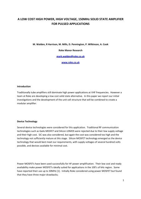
A Low Cost High Power, High Voltage, 150MHz Solid State Amplifier ...
A Low Cost High Power, High Voltage, 150MHz Solid State Amplifier ...
A Low Cost High Power, High Voltage, 150MHz Solid State Amplifier ...

You also want an ePaper? Increase the reach of your titles
YUMPU automatically turns print PDFs into web optimized ePapers that Google loves.
A LOW COST HIGH POWER, HIGH VOLTAGE, <strong>150MHz</strong> SOLID STATE AMPLIFIER<br />
FOR PULSED APPLICATIONS<br />
M. Walden, R Harrison, M. Mills, D. Pennington, P. Wilkinson, A. Cook<br />
Roke Manor Research<br />
mark.walden@roke.co.uk<br />
www.roke.co.uk<br />
Introduction<br />
Traditionally tube amplifiers still dominate high power applications at VHF frequencies. However a<br />
team at Roke are developing a low cost solid state alternative. In this paper we report our initial<br />
investigations and the development of the unit cell structure that will be combined to create a<br />
modular amplifier.<br />
Device Technology<br />
Several device technologies were considered for this application. Traditional RF communication<br />
technologies such as GaAs MESFET and Silicon LDMOS were rejected due to their low supply voltage<br />
and their high cost. SiC was also considered, but again the cost was considered too high and the<br />
technology not sufficiently mature at this stage. Silicon MOSFET technology emerged as the device<br />
technology that would best meet our requirements, with supply voltages of several hundred volts<br />
possible, and devices available for minimal cost.<br />
<strong>Power</strong> MOSFETs have been used successfully for HF power amplification. Their low cost and ready<br />
availability make power MOSFETs ideally suited for applications in the 100’s of kHz region. Some<br />
have reported their use up to 30MHz [1]. Initially Roke considered using power MOSFET but found<br />
that they have three major drawbacks;<br />
1
1. high input capacitances – leading to low switching speed<br />
2. device integration (having drain connected to heat sink)<br />
3. packaging - long leads leading to high inductances<br />
Some effort has been made by certain device manufacturers to address some of these problems, but<br />
never, it seems, all of them at the same time!<br />
However all was not lost. Before the advent of LDMOS, Motorola used to champion a series of VHF<br />
RF MOSFETs, the most popular of which was the MRF150 [2]. Indeed they provided an application<br />
note for building a 600W 30MHz amplifier from four such devices [3]. If these devices were available<br />
in the early 1980s, we reasoned, then what was the state of the art today nearly 30 years later<br />
After some searching, we found that the natural successor to the MRF150 was being produced by<br />
the Microsemi Corporation (http://www.microsemi.com/).<br />
Microsemi offer several different RF MOSFETs. It is quite interesting to look at each part in turn and<br />
to realise that they attempted to solve the main problems with power MOSFETs one at a time.<br />
Though the input impedances of their devices are still relatively high, the gate structures have been<br />
modified to be more forgiving at VHF frequencies. Also they have isolated the drain from the<br />
heatsink, attaching the source instead in a manner more in keeping with RF design (Frey [4] gives an<br />
interesting account of how to overcome this issue with traditional MOSFETs by simply wiring it into<br />
the circuit the “wrong way round”). Finally they have adopted packages more suited to RF<br />
applications.<br />
2
Topology<br />
We had decided upon a push-pull configuration. This presents its own challenges for the device<br />
selection. Unless “mirror image” devices are available, the layout of the amplifier will be<br />
compromised. An alternative is to use a device that consists of two die in a single package.<br />
Microsemi offers such a device in the ARF475FL [5].<br />
Microsemi also offer a reference design for the ARF475FL at 128MHz [6]. Using this as a starting<br />
point Roke designed an amplifier more fitting for our purpose. Several changes to the reference<br />
design were enabled. Our requirement was for fast, short pulses, at low duty cycle. We reasoned<br />
that the gate and drain bias circuitry described in the technical note would not support this.<br />
Furthermore we wished to control the device such that it was not active during the “off” period. We<br />
would use a limited charge storage arrangement to provide the DC bias, and turning the device off<br />
would give time for the capacitors used to recharge before the next burst was required. Usually we<br />
would use high side switching to control the device, but in this case, with drain voltages of over 150V<br />
present we decided to control the device by use of the gate bias to achieve pinch off. The ARF475FL<br />
is pinched off at 0V, but to be sure we arranged for the gate bias to be made negative during the off<br />
period.<br />
The control pulse was provided by a PIC microcontroller, programmed to give various length pulses<br />
and PRIs, controlled by DIP switches. The output of this was buffered using open collector and fed<br />
to a driver MOSFET. This was arranged such that in the off period the device output -5V and during<br />
the on pulse it output the gate bias as set by a PSU. Local charge storage and RF decoupling of the<br />
drain supply line was provided by AVXs high voltage MLC chip capacitors with X7R dielectric. Bulk<br />
storage capacitance was provided by AVX FFVE series polyester capacitors.<br />
For testing purposes the amplifier was placed inside an interlocked safety box. This also contained<br />
the charging/discharging circuitry for the storage capacitors, and limited the available energy to safe<br />
levels. Figure 1 shows the key parts of the amplifier design.<br />
3
Figure 1: The high power high voltage solid state amplifier<br />
4
Results<br />
Using their reference design [6] for 128MHz operation, Microsemi were able to demonstrate a<br />
maximum output power for the ARFL475 device of just over 1kW. Using the board designed at Roke<br />
we were able to demonstrate in excess of 2kW at the same frequency. However our target<br />
frequency was <strong>150MHz</strong>. The bandwidth of the device was measured, and found that the gain at<br />
<strong>150MHz</strong> was less than half that of the 128MHz.<br />
Figure 2: The gain of the amplifier in its original circuit<br />
5
The design was tweaked to increase the gain at <strong>150MHz</strong> to be comparable to that of the original<br />
circuit at 128MHz. The power performance of the device was then measured at <strong>150MHz</strong> and found<br />
to be in excess of 2kW.<br />
Figure 3: <strong>Power</strong> sweep measurements for the modified amplifier at <strong>150MHz</strong><br />
6
Next Steps<br />
Having successfully demonstrated over 2kW from a single device, the next step is to combine several<br />
devices to make a more powerful module. A block diagram of this module is illustrated in Figure 4.<br />
A development to progress towards this scale of module is already underway. Ultimately it will<br />
include advances such as pulse, gate, and drain conditioning hardware on the board to make a more<br />
integrated module.<br />
Pulse<br />
Generation<br />
and Control<br />
Circuitry<br />
Single<br />
ended to<br />
push pull<br />
conversion<br />
network<br />
Bias Control<br />
Circuitry<br />
ARF475FL<br />
4-way<br />
splitter and<br />
interstage<br />
matching<br />
network<br />
4-way<br />
splitter and<br />
interstage<br />
matching<br />
network<br />
ARF475FL ARF475FL ARF475FL ARF475FL<br />
Push pull to<br />
single ended<br />
conversion<br />
network<br />
Push pull to<br />
single ended<br />
conversion<br />
network<br />
Push pull to<br />
single ended<br />
conversion<br />
network<br />
Push pull to<br />
single ended<br />
conversion<br />
network<br />
4-way<br />
combiner<br />
network<br />
Figure 4: Block diagram for a high power module<br />
7
Conclusion<br />
A low cost, high power, high voltage solid state amplifier has been demonstrated. The amplifier uses<br />
commercially available MOSFET devices to achieve high output powers at low component cost. Over<br />
2kW of pulsed power has been obtained with power gain in excess of 15dB. The amplifier is being<br />
used as the unit cell for a high power modular amplifier, which is currently under development at<br />
Roke.<br />
References<br />
[1] Mike Kossor; A Broadband HF <strong>Amplifier</strong> Using <strong>Low</strong>-<strong>Cost</strong> <strong>Power</strong> MOSFETs; QST Magazine;<br />
March and April 1999.<br />
[2] MRF150 Datasheet<br />
[3] Motorola EB104<br />
[4] Richard Frey; Capabilities of <strong>Low</strong>-cost <strong>High</strong> <strong>Voltage</strong> RF <strong>Power</strong> MOSFETs at HF and VHF;<br />
Technical Brief APTB 981<br />
[5] ARF475FL Datasheet<br />
[6] Richard Frey; ARF475FL 128 MHz Linear Pulse <strong>Amplifier</strong>; Application Note APT06010<br />
8