A HIGH LINEARITY FMCW SWEEP GENERATOR
A HIGH LINEARITY FMCW SWEEP GENERATOR
A HIGH LINEARITY FMCW SWEEP GENERATOR

Create successful ePaper yourself
Turn your PDF publications into a flip-book with our unique Google optimized e-Paper software.
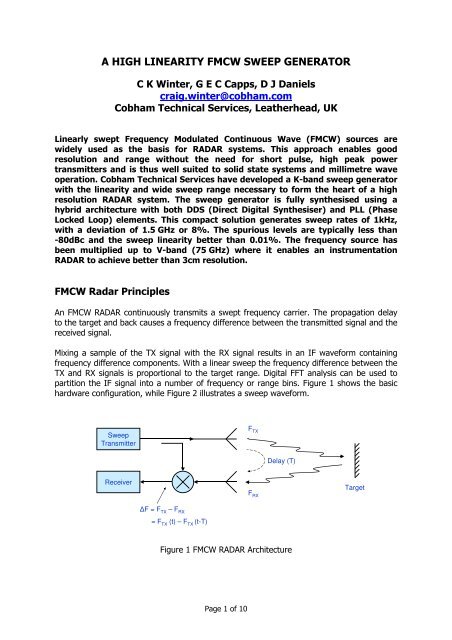
A <strong>HIGH</strong> <strong>LINEARITY</strong> <strong>FMCW</strong> <strong>SWEEP</strong> <strong>GENERATOR</strong>C K Winter, G E C Capps, D J Danielscraig.winter@cobham.comCobham Technical Services, Leatherhead, UKLinearly swept Frequency Modulated Continuous Wave (<strong>FMCW</strong>) sources arewidely used as the basis for RADAR systems. This approach enables goodresolution and range without the need for short pulse, high peak powertransmitters and is thus well suited to solid state systems and millimetre waveoperation. Cobham Technical Services have developed a K-band sweep generatorwith the linearity and wide sweep range necessary to form the heart of a highresolution RADAR system. The sweep generator is fully synthesised using ahybrid architecture with both DDS (Direct Digital Synthesiser) and PLL (PhaseLocked Loop) elements. This compact solution generates sweep rates of 1kHz,with a deviation of 1.5 GHz or 8%. The spurious levels are typically less than-80dBc and the sweep linearity better than 0.01%. The frequency source hasbeen multiplied up to V-band (75 GHz) where it enables an instrumentationRADAR to achieve better than 3cm resolution.<strong>FMCW</strong> Radar PrinciplesAn <strong>FMCW</strong> RADAR continuously transmits a swept frequency carrier. The propagation delayto the target and back causes a frequency difference between the transmitted signal and thereceived signal.Mixing a sample of the TX signal with the RX signal results in an IF waveform containingfrequency difference components. With a linear sweep the frequency difference between theTX and RX signals is proportional to the target range. Digital FFT analysis can be used topartition the IF signal into a number of frequency or range bins. Figure 1 shows the basichardware configuration, while Figure 2 illustrates a sweep waveform.SweepTransmitterF TXDelay (T)ReceiverF RXTarget∆F = F TX– F RX= F TX(t) – F TX(t-T)Figure 1 <strong>FMCW</strong> RADAR ArchitecturePage 1 of 10
Phase AccumulatorFrequencyWord32Σ3219(MSBs)Look Up TableA=SinΦPhaseToAmplitude14DACDigitalToAnalogueOutputClock1 GHzΦAAccumulatingphaseQuantised phasesFigure 5 DDS Synthesiser CoreThe Analog Devices AD9910 is a flexible, high speed, single chip DDS solution. It is capableof generating frequencies from 0 Hz up to approximately 400 MHz using the maximum1 GHz clock. The frequency is inherently very accurate due to the high resolution 32 bitprocessing. Because it is a sampled and quantised system the output spectrum containssignificant spurious products, typically at levels around -55 dBc.Figure 6 Typical DDS Spectrum (from Analog Devices AD9910 data sheet)Page 5 of 10
An extension to the basic DDS core enables generation of extremely accurate frequencyramps. By using some additional logic the frequency word controlling the instantaneousfrequency of the DDS core can be varied linearly with a ramp. The logic sets the start andstop frequencies and manages the switch between ramping up or down.Frequency accumulator32Inc.SelectorΣEnd pointlogic32DDS CoreFMSweepDec.Slopesettings32FrequencyWord to DDSClock1 GHz÷ 4Figure 7 DDS With Frequency RampIn the case of The Analog Devices AD9910, the DDS internally updates the frequency every4 clock cycles, or 4ns. This equates to 250,000 discrete steps within a 1 ms frequencysweep.Hybrid SynthesiserTwo key features of the architecture are:Minimum DDS multiplication factor by use of frequency translation and,Integrated tracking filter function to smooth steps and reduce DDS spurious levels.Minimising DDS Frequency MultiplicationFrequency multiplication increases the level of spurious signals by an amount equal to20log(n) where n is the multiplication factor. Thus one of the key design aims for the hybridsynthesiser is to use the lowest practical DDS frequency multiplication factor (in this casex8). This means dissociating sweep bandwidth and centre frequency so that both aspectscan be dealt with independently. In the architecture of Figure 8 the DDS provides thereference input to a modified PLL system. The feedback path of the PLL includes a divider toachieve the required closed loop bandwidth multiplication. To achieve the desired outputfrequency (18.75 GHz) the feedback path of the PLL also includes a fixed frequencydownconverter. The downconverter within the feedback path effectively adds an offsetfrequency to the final VCO output.Page 6 of 10
133 to 320.5 MHzDDS(swept)Loop filterVCO18 to 19.5 GHz1.064 to 2.564 GHz133 to 320.5 MHz÷ 8BPFBandwidth ScalingFrequencyOffsetLOSynth.16.936 GHzFigure 8 Hybrid SynthesiserTracking filterIn an ideal situation the output from the VCO does not contain any non-harmonic spurii.However, in practice, unwanted signals reach the VCO control port and the resultingmodulation causes spurious sidebands at the VCO RF output. The low pass loop filter isdesigned to minimise the bandwidth of the spurious modulation while maintaining adequateloop dynamics. From the DDS’s perspective the PLL appear as a tracking filter. The PLLtracks the reference input frequency and the low pass loop filter limits the bandwidth of theVCO control signal such that the unwanted sidebands are constrained to a narrow,symmetrical bandwidth around the carrier. The combination of fast DDS frequency update(4ns) and relatively low PLL loop bandwidth (200 kHz) effectively eliminates any granularityin the output. At carrier offsets less than the loop bandwidth the DDS spurious levels areincreased by 18dB (to typically -37 dBc) due to the multiplication factor (x8). For offsetsgreater than the loop bandwidth the DDS spurii are progressively attenuated. Appropriatechoice of loop filter bandwidth, in this case around 200kHz, means that most of the spuriouscomponents in the output of the DDS (up to 400MHz) are attenuated and the end result isan extremely clean wideband spectrum.Page 7 of 10
Spurious levels better than -80dBc are easily achieved over broad bandwidths. Thebroadband noise floor of Figure 9 is the spectrum analyser measurement limit, with nosynthesiser spurious components visible.Figure 9 Wideband SpectrumThe major DDS spurious frequency components are not fixed but are related to DDS outputfrequency. In this case, with a swept frequency output, unfiltered spurious componentswithin 200kHz of the carrier exist for just a very small part of the sweep and thus are ofminimal significance when their overall contribution is considered. Figure 10 shows the closeto carrier spectrum dominated by phase noise with two small discrete spurious signals at+/- 1.5MHz offset.Figure 10 Phase NoisePage 8 of 10
Figure 11 shows the VCO control voltage in purple and the loop error (phase discriminatoroutput) in red. The control voltage is essentially triangular, reflecting the up/down sweeppattern, but sharp eyes might just notice that the sides are not straight because of thenon-linearity of the VCO transfer function. The error voltage confirms that the loop is phaselocked throughout the whole cycle and the VCO is tracking the DDS. The error is normallyzero except at the slope transitions when the error briefly spikes but remains less than 180º,monotonic and non-saturated.Figure 11 VCO Control Voltage and Loop Error VoltagemmWave Radar SystemThe hybrid synthesiser module has been built into a short range instrumentation RADARincorporating a further x4 frequency multiplier to reach 75 GHz with a 6 GHz bandwidth. Thereturn signals are processed using a custom DSP based FFT processor.18 to 19.5 GHzHybridsynthesiserX 472 to 78 GHzTXFFTProcessorIF ReceiverRX0 to 8 MHz0 to 200 m rangeAnalogue +A to D conversionFigure 12 mmWave Radar SystemPage 9 of 10
A simple laboratory test was carried out with a metal target placed on a particle board andfoam support table. An example response is shown in Figure 13. The test target return canbe clearly identified at 1904 cm. Also clearly visible are returns from the front and backedges of the support structure at around 1870 and 1944 cm.TargetSupport structureSupport structureFigure 13 Typical Target ReturnConclusionsThe PLL/DDS Hybrid Synthesiser has demonstrated excellent performance:High linearityLow spurious levelsFlexible ArchitectureRe-configurableNo calibration: