SiT1532 - SiTime
SiT1532 - SiTime
SiT1532 - SiTime

Create successful ePaper yourself
Turn your PDF publications into a flip-book with our unique Google optimized e-Paper software.
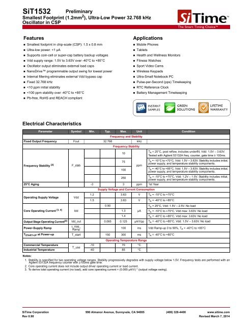
<strong>SiT1532</strong><br />
Preliminary<br />
Smallest Footprint (1.2mm 2 ), Ultra-Low Power 32.768 kHz<br />
Oscillator in CSP<br />
The Smart Timing Choice<br />
The Smart Timing Choice<br />
Features<br />
• Smallest footprint in chip-scale (CSP): 1.5 x 0.8 mm<br />
• Ultra-low power:
<strong>SiT1532</strong><br />
Smallest Footprint (1.2mm 2 ), Ultra-Low Power 32.768 kHz<br />
Oscillator in CSP<br />
The Smart Timing Choice<br />
The Smart Timing Choice<br />
Electrical Characteristics (continued)<br />
Parameter Symbol Min. Typ. Max. Unit Condition<br />
LVCMOS Output Option, T A = -40°C to +85°C, typical values are at T A = 25°C<br />
Output Rise/Fall Time tr, tf 100 200 ns 10-90%, 15 pF load, Vdd = 1.5V to 3.63V<br />
Output Clock Duty Cycle DC 48 52 %<br />
Output Voltage High VOH 90% V Vdd: 1.5V – 3.63V. I OH = -10 μA, 15 pF<br />
Output Voltage Low VOL 10% V Vdd: 1.5V – 3.63V. I OL = 10 μA, 15 pF<br />
NanoDrive Programmable, Reduced Swing Output<br />
Output Rise/Fall Time tf, tf 200 ns 30-70%, 10 pF Load<br />
Output Clock Duty Cycle DC 48 52 %<br />
AC-coupled Programmable<br />
Output Swing<br />
DC-Biased Programmable<br />
Output Voltage High Range<br />
DC-Biased Programmable<br />
Output Voltage Low Range<br />
Programmable Output Voltage<br />
Swing Tolerance<br />
V_sw<br />
VOH<br />
VOL<br />
0.20 to<br />
0.80<br />
0.60 to<br />
1.225<br />
0.35 to<br />
0.80<br />
-0.055 0.055 V<br />
V<br />
V<br />
V<br />
<strong>SiT1532</strong> does not internally AC-couple. This output description<br />
is intended for a receiver that is AC-coupled. See Table 2 for<br />
acceptable NanoDrive swing options.<br />
Vdd: 1.5V – 3.63V, 10 pF Load, I OH / I OL = ±0.2 μA.<br />
Vdd: 1.5V – 3.63V. I OH = -0.2 μA, 10 pF Load. See Table 1 for<br />
acceptable V OH /V OL setting levels.<br />
Vdd: 1.5V – 3.63V. I OL = 0.2 μA, 10 pF Load. See Table 1 for<br />
acceptable V OH /V OL setting levels.<br />
T A = -40°C to +85°C, Vdd = 1.5V to 3.63V. See Tables 1 and -2<br />
for acceptable NanoDrive Settings.<br />
Period Jitter T_jitt 35 ns RMS N = 10,000, T A = 25°C, Vdd = 1.5V – 3.63V<br />
Pin Configuration<br />
Pin Symbol I/O Functionality<br />
1, 4 GND<br />
Power Supply<br />
Ground<br />
2 CLK Out OUT<br />
3 Vdd Power Supply<br />
Connect to ground. Acceptable to connect pin 1 and 4 together. Both pins<br />
must be connected to GND.<br />
Oscillator clock output. The CLK can drive into a Ref CLK input or into an<br />
ASIC or chip-set’s 32kHz XTAL input. When driving into an ASIC or<br />
chip-set oscillator input (X IN and X Out), the CLK Out is typically<br />
connected directly to the XTAL IN pin. No need for load<br />
capacitors. The output driver is intended to be insensitive to capacitive<br />
loading.<br />
Connect to power supply 1.2V ≤ Vdd ≤ 3.63V. Under normal operating<br />
conditions, Vdd does not require external bypass/decoupling<br />
capacitor(s). For more information about the internal power-supply<br />
filtering, see the Power Supply Noise Immunity section in the detailed<br />
description.<br />
Contact factory for applications that require a wider operating supply<br />
voltage range.<br />
CSP Package (Top View)<br />
GND 1 4 GND<br />
CLK Out 2 3 Vdd<br />
Rev. 0.90 Page 2 of 10 www.sitime.com
<strong>SiT1532</strong><br />
Smallest Footprint (1.2mm 2 ), Ultra-Low Power 32.768 kHz<br />
Oscillator in CSP<br />
The Smart Timing Choice<br />
The Smart Timing Choice<br />
System Block Diagram<br />
MEMS Resonator<br />
GND<br />
Control<br />
Regulators<br />
Vdd<br />
Trim<br />
Prog<br />
Prog<br />
GND<br />
Sustaining<br />
Amp<br />
Ultra-Low<br />
Power<br />
PLL<br />
Divider<br />
Ultra-Low<br />
Power Driver<br />
CLK Out<br />
Figure 1.<br />
Absolute Maximum<br />
Attempted operation outside the absolute maximum ratings of may cause permanent damage to the part. Actual performance of<br />
the IC is only guaranteed within the operational specifications, not at absolute maximum ratings.<br />
Parameter Test Condition Value Unit<br />
Continuous Power Supply Voltage Range (Vdd) -0.5 to 3.63 V<br />
Short Duration Maximum Power Supply Voltage (Vdd)
<strong>SiT1532</strong><br />
Smallest Footprint (1.2mm 2 ), Ultra-Low Power 32.768 kHz<br />
Oscillator in CSP<br />
The Smart Timing Choice<br />
The Smart Timing Choice<br />
Description<br />
The <strong>SiT1532</strong> is the world’s smallest, lowest power 32 kHz<br />
oscillator optimized for mobile and other battery-powered<br />
applications. <strong>SiTime</strong>’s silicon MEMS technology enables the<br />
smallest footprint and chip-scale packaging. This device<br />
reduces the 32 kHz footprint by as much as 85% compared to<br />
existing 2.0 x 1.2 mm SMD XTAL packages. Unlike XTALs, the<br />
<strong>SiT1532</strong> oscillator output enables greater component<br />
placement flexibility and eliminates external load capacitors,<br />
thus saving additional component count and board space. And<br />
unlike standard oscillators, the <strong>SiT1532</strong> features<br />
NanoDrive, a factory programmable output that reduces the<br />
voltage swing to minimize power.<br />
The 1.2V to 3.63V operating supply voltage range makes it an<br />
ideal solution for mobile applications that incorporate a<br />
low-voltage, battery-back-up source such as a coin-cell or<br />
super-cap.<br />
<strong>SiTime</strong>’s MEMS oscillators consist of MEMS resonators and a<br />
programmable analog circuit. Our MEMS resonators are built<br />
with <strong>SiTime</strong>’s unique MEMS First process. A key manufacturing<br />
step is EpiSeal during which the MEMS resonator is<br />
annealed with temperatures over 1000°C. EpiSeal creates an<br />
extremely strong, clean, vacuum chamber that encapsulates<br />
the MEMS resonator and ensures the best performance and<br />
reliability. During EpiSeal, a poly silicon cap is grown on top of<br />
the resonator cavity, which eliminates the need for additional<br />
cap wafers or other exotic packaging. As a result, <strong>SiTime</strong>’s<br />
MEMS resonator die can be used like any other semiconductor<br />
die. One unique result of <strong>SiTime</strong>’s MEMS First and<br />
EpiSeal manufacturing processes is the capability to integrate<br />
<strong>SiTime</strong>’s MEMS die with a SOC, ASIC, microprocessor or<br />
analog die within a package to eliminate external timing<br />
components and provide a highly integrated, smaller, cheaper<br />
solution to the customer.<br />
Frequency Stability<br />
The <strong>SiT1532</strong> is factory calibrated (trimmed) to guarantee<br />
frequency stability to be less than 10 ppm at room temperature<br />
and less than 100 ppm over the full -40°C to +85°C temperature<br />
range. Unlike quartz crystals that have a classic tuning<br />
fork parabola temperature curve with a 25°C turnover point,<br />
the <strong>SiT1532</strong> temperature coefficient is extremely flat across<br />
temperature. The device maintains less than 100 ppm<br />
frequency stability over the full operating temperature range<br />
when the operating voltage is between 1.5 and 3.63V.<br />
When measuring the <strong>SiT1532</strong> output frequency with a<br />
frequency counter, it is important to make sure the counter's<br />
gate time is >100ms. The slow frequency of a 32kHz clock will<br />
give false readings with faster gate times.<br />
Contact <strong>SiTime</strong> for applications that require a wider supply<br />
voltage range >3.63V or lower frequency options as low as<br />
1Hz.<br />
Power Supply Noise Immunity<br />
In addition to eliminating external output load capacitors<br />
common with standard XTALs, The <strong>SiT1532</strong> includes special<br />
internal power supply filtering and thus, eliminates the need<br />
for an external Vdd bypass-decoupling capacitor. This feature<br />
further simplifies the design and keeps the footprint as small<br />
as possible. Internal power supply filtering is designed to<br />
reject greater than ±150 mVpp magnitude and frequency<br />
components through 10 MHz.<br />
Output Voltage<br />
The <strong>SiT1532</strong> has two output voltage options. One option is a<br />
standard LVCMOS output swing. The second option is the<br />
NanoDrive reduced swing output. Output swing is customer<br />
specific and programmed between 200 mV and 800 mV. For<br />
DC-coupled applications, output V OH and V OL are individually<br />
factory programmed to the customers’ requirement. V OH<br />
programming range is between 600 mV and 1.225V in 100 mV<br />
increments. Similarly, V OL programming range is between 350<br />
mV and 800 mV. For example; a PMIC or MCU is internally<br />
1.8V logic compatible, and requires a 1.2V V IH and a 0.6V V IL .<br />
Simply select <strong>SiT1532</strong> NanoDrive factory programming code<br />
to be “D14” and the correct output thresholds will match the<br />
downstream PMIC or MCU input requirements. Interface logic<br />
will vary by manufacturer and we recommend that you review<br />
the input voltage requirements for the input interface.<br />
For DC-biased NanoDrive output configuration, the minimum<br />
V OL is limited to 350mV and the maximum allowable swing<br />
(V OH - V OL ) is 750mV. For example, 1.1V V OH and 400mV V OL<br />
is acceptable, but 1.2V V OH and 400 mV V OL is not<br />
acceptable.<br />
When the output is interfacing to an XTAL input that is internally<br />
AC-coupled, the <strong>SiT1532</strong> output can be factory<br />
programmed to match the input swing requirements. For<br />
example, if a PMIC or MCU input is internally AC-coupled and<br />
requires an 800mV swing, then simply choose the <strong>SiT1532</strong><br />
NanoDrive programming code “AA8” in the part number. It is<br />
important to note that the <strong>SiT1532</strong> does not include internal<br />
AC-coupling capacitors. Please see the Part Number Ordering<br />
section at the end of the datasheet for more information about<br />
the part number ordering scheme.<br />
Power-up<br />
The <strong>SiT1532</strong> starts-up to a valid output frequency within 300<br />
ms (150ms typ). To ensure proper start-up, Vdd power-supply<br />
ramp, from a power-down state to 90% of final Vdd, must be<br />
less than 100 ms.<br />
Rev. 0.90 Page 4 of 10 www.sitime.com
<strong>SiT1532</strong><br />
Smallest Footprint (1.2mm 2 ), Ultra-Low Power 32.768 kHz<br />
Oscillator in CSP<br />
The Smart Timing Choice<br />
The Smart Timing Choice<br />
<strong>SiT1532</strong> NanoDrive<br />
Figure 2 shows a typical output waveform of the <strong>SiT1532</strong> (into<br />
a 10 pF load) when factory programmed for a 0.70V swing and<br />
DC bias (V OH /V OL ) for 1.8V logic:<br />
Example:<br />
• NanoDrive part number coding: D14. Example part<br />
number: <strong>SiT1532</strong>AI-J4-D14-32.768<br />
•V OH = 1.1V, V OL = 0.4V (V sw = 0.70V)<br />
VOH = 1.1V<br />
VSW = 0.7V<br />
VOL = 0.4V<br />
For these applications, refer to Table 2 for the acceptable<br />
voltage swing options.<br />
Table 2. Acceptable AC-Coupled Swing Levels<br />
Swing 0.800 0.700 0.600 0.500 0.400 0.300 0.250 0.200<br />
Output<br />
Code<br />
AA8 AA7 AA6 AA5 AA4 AA3 AA2 AA1<br />
Example:<br />
• NanoDrive part number coding: AA2. Example part number:<br />
<strong>SiT1532</strong>AI-J4-AA2-32.768<br />
• Output voltage swing: 0.250V<br />
The values listed in Tables 1 and -2 are nominal values at<br />
25°C and will exhibit a tolerance of ±55 mV across Vdd and<br />
-40°C to 85°C operating temperature range.<br />
<strong>SiT1532</strong> Full Swing LVCMOS Output<br />
The <strong>SiT1532</strong> can be factory programmed to generate<br />
full-swing LVCMOS levels. Figure 3 shows the typical<br />
waveform (Vdd = 1.8V) at room temperature into a 15 pF load.<br />
Figure 2. <strong>SiT1532</strong>AI-J4-D14-32.768<br />
Output Waveform (10 pF load)<br />
Table 1 shows the supported NanoDrive V OH , V OL factory<br />
programming options.<br />
Table 1. Acceptable V OH /V OL NanoDrive Levels<br />
V OL /V OH 1.225 1.100 1.000 0.900 0.800 0.700 0.600<br />
0.800 D28 D18 D08<br />
0.700 D27 D17 D07 D97<br />
0.525 D26 D16 D06 D96 D86<br />
0.500 D25 D15 D05 D95 D85 D75<br />
0.400 D14 D04 D94 D84 D74 D64<br />
0.350 D13 D03 D93 D83 D73 D63<br />
Table 2 shows the supported AC coupled Swing levels. The<br />
“AC-coupled” terminology refers to the programming<br />
description for applications where the downstream chipset<br />
includes an internal AC-coupling capacitor, and therefore,<br />
only the output swing is important and V OH /V OL is not relevant.<br />
Figure 3. LVCMOS Waveform<br />
(Vdd = 1.8V) into 15 pF Load<br />
Example:<br />
• LVCMOS output part number coding is always DCC<br />
• Example part number: <strong>SiT1532</strong>AI-J4-DCC-32.768<br />
Rev. 0.90 Page 5 of 10 www.sitime.com
<strong>SiT1532</strong><br />
Smallest Footprint (1.2mm 2 ), Ultra-Low Power 32.768 kHz<br />
Oscillator in CSP<br />
Calculating Load Current<br />
No Load Supply Current<br />
When calculating no-load power for the <strong>SiT1532</strong>, the core and<br />
output driver components need to be added. Since the output<br />
voltage swing can be programmed for reduced swing between<br />
250 mV and 800 mV for ultra-low power applications, the<br />
output driver current is variable. Therefore, no-load operating<br />
supply current is broken into two sections; core and output<br />
driver. The equation is as follows:<br />
Total Supply Current (no load) = I dd Core + (65nA/V)(Vout pp )<br />
Example 1: Full-swing LVCMOS<br />
• Vdd = 1.8V<br />
• Idd Core = 900nA (typ)<br />
•Vout pp = 1.8V<br />
Supply Current = 900nA + (65nA/V)(1.8V) = 1017nA<br />
Example 2: NanoDrive Reduced Swing<br />
• Vdd = 1.8V<br />
• Idd Core = 900nA (typ)<br />
•Vout pp (Programmable) = V OH – V OL = 1.1V - 0.6V = 500mV<br />
Supply Current = 900nA + (65nA/V)(0.5V) = 932nA<br />
The Smart Timing Choice<br />
The Smart Timing Choice<br />
Total Supply Current with Load<br />
To calculate the total supply current, including the load, follow<br />
the equation listed below. Note the 30% reduction in power<br />
with NanoDrive.<br />
Total Current = Idd Core + Idd Output Driver (65nA/V*Vout pp )<br />
+ Load Current (C*V*F)<br />
Example 1: Full-swing LVCMOS<br />
• Vdd = 1.8V<br />
• Idd Core = 900nA<br />
• Load Capacitance = 10pF<br />
• Idd Output Driver: (65nA/V)(1.8V) = 117nA<br />
• Load Current: (10pF)(1.8V)(32.768kHz) = 590nA<br />
• Total Current = 900nA + 117nA + 590nA = 1.6µA<br />
Example 2: NanoDrive Reduced Swing<br />
• Vdd = 1.8V<br />
• Idd Core = 900nA<br />
• Load Capacitance = 10pF<br />
•Vout pp (Programmable): V OH – V OL = 1.1V - 0.6V = 500mV<br />
• Idd Output Driver: (65nA/V)(0.5V) = 33nA<br />
• Load Current: (10pF)(0.5V)(32.768kHz) = 164nA<br />
• Total Current = 900nA + 33nA + 164nA = 1.1µA<br />
Rev. 0.90 Page 6 of 10 www.sitime.com
<strong>SiT1532</strong><br />
Smallest Footprint (1.2mm 2 ), Ultra-Low Power 32.768 kHz<br />
Oscillator in CSP<br />
The Smart Timing Choice<br />
The Smart Timing Choice<br />
Typical Operating Curves<br />
(T A = 25°C, Vdd = 1.8V, unless otherwise stated)<br />
30<br />
Initial Tolerance Histogram<br />
NanoDrive Output Waveform<br />
(V OH = 1.1V, V OL = 0.4V; <strong>SiT1532</strong>AI-J4-D14-32.768)<br />
Number of Devices<br />
25<br />
20<br />
(TA = 25°C)<br />
15<br />
10<br />
Min/Max Limit<br />
VOH = 1.1V<br />
VSW = 0.7V<br />
5<br />
VOL = 0.4V<br />
-15 -10 -5 0 5 10 15<br />
Initial Tolerance (ppm)<br />
LVCMOS Output Waveform<br />
(<strong>SiT1532</strong>AI-J4-DCC-32.768)<br />
Rev. 0.90 Page 7 of 10 www.sitime.com
<strong>SiT1532</strong><br />
Smallest Footprint (1.2mm 2 ), Ultra-Low Power 32.768 kHz<br />
Oscillator in CSP<br />
Dimensions and Patterns<br />
1.55 x 0.85 mm CSP<br />
Package Size – Dimensions (Unit: mm)<br />
The Smart Timing Choice<br />
The Smart Timing Choice<br />
Recommended Land Pattern (Unit: mm)<br />
1.55 ±0.02<br />
#4 #3<br />
0.85 ±0.02<br />
#3 #4<br />
#4<br />
#3<br />
0.315 ±0.015<br />
#1 #2<br />
#2 #1<br />
#1<br />
#2<br />
Rev. 0.90 Page 8 of 10 www.sitime.com
<strong>SiT1532</strong><br />
Smallest Footprint (1.2mm 2 ), Ultra-Low Power 32.768 kHz<br />
Oscillator in CSP<br />
Ordering Information<br />
The Smart Timing Choice<br />
The Smart Timing Choice<br />
Part number characters in blue represent the customer specific options. The other characters in the part number are fixed.<br />
The following examples illustrate how to select<br />
the appropriate temp range and output voltage<br />
requirements:<br />
Example 1: <strong>SiT1532</strong>AI-J4-D14-32.768<br />
• Industrial temp & corresponding 100 ppm<br />
frequency<br />
stability. Note, 100 ppm is only available for<br />
the industrial temp range, and 75 ppm is<br />
only available for the commercial temp<br />
range.<br />
• Output swing requirements:<br />
a) “D” = DC-coupled receiver<br />
b) “J” = CSP<br />
b) “1” = V OH = 1.1V<br />
Example 2: <strong>SiT1532</strong>AC-J5-AA5-32.768<br />
• Commercial temp & corresponding 75 ppm<br />
frequency stability. Note, 100 ppm is only<br />
available for the industrial temp range, and<br />
75 ppm is only available for the commercial<br />
temp range.<br />
• Output swing requirements:<br />
a) “A” = AC-coupled receiver<br />
b) “A” = AC-coupled receiver<br />
c) “5” = 500mV swing<br />
c) “4” = V OL = 0.4V<br />
Acceptable AC-Coupled Swing Levels<br />
Part Family<br />
“<strong>SiT1532</strong>”<br />
Revision Letter<br />
“A”: is the revision<br />
Temperature Range<br />
“C”: Commercial, -10 to 70ºC<br />
“I”: Industrial, -40 to 85ºC<br />
Package Size<br />
1.5 mm x 0.8 mm CSP<br />
Frequency Stability<br />
Swing 0.800 0.700 0.600 0.500 0.400 0.300 0.250 0.200<br />
Output<br />
Code<br />
AA8 AA7 AA6 AA5 AA4 AA3 AA2 AA1<br />
Acceptable V OH /V OL NanoDrive Levels<br />
V OL /V OH 1.225 1.100 1.000 0.900 0.800 0.700 0.600<br />
0.800 D28 D18 D08<br />
0.700 D27 D17 D07 D97<br />
0.525 D26 D16 D06 D96 D86<br />
0.500 D25 D15 D05 D95 D85 D75<br />
0.400 D14 D04 D94 D84 D74 D64<br />
0.350 D13 D03 D93 D83 D73 D63<br />
“5”: ±75 PPM (-10 to 70ºC only)<br />
“4”: ±100 PPM (-40 to 85ºC only)<br />
AC- or DC-coupled<br />
“A”: AC-coupled Signal Path Rx<br />
“D”: DC-coupled Signal Path or<br />
Rail-to-Rail LVCMOS<br />
<strong>SiT1532</strong>AI-J4-D14-32.768S<br />
Packaging<br />
“S”: 8 mm Tape & Reel, 10ku reel<br />
“D”: 8 mm Tape & Reel, 3ku reel<br />
“E”: 8 mm Tape & Reel, 1ku reel<br />
Samples in cut Tape & Reel strips<br />
Output Clock Frequency<br />
32.768 kHz<br />
DC-coupled Output VOL or AC Swing<br />
(refer to Table 3 below for available<br />
options)<br />
“1”: 200mV (Only available for<br />
AC-coupled swing option)<br />
“2”: 250mV (Only available for<br />
AC-coupled swing option)<br />
“3”: 350mV<br />
“4”: 400mV<br />
“5”: 500mV<br />
“6”: 600mV<br />
“7”: 700mV<br />
“8”: 800mV<br />
“C”: rail-to-rail LVCMOS<br />
DC-coupled Output VOH (refer to<br />
Table 4 below for available options)<br />
“6”: 600mV<br />
“7”: 700mV<br />
“8”: 800mV<br />
“9”: 900mV<br />
“0”: 1.00V<br />
“1”: 1.10V<br />
“2”: 1.225V<br />
“A”: AC-coupled Receiver<br />
“C”: rail-to-rail LVCMOS<br />
© <strong>SiTime</strong> Corporation 2014. The information contained herein is subject to change at any time without notice. <strong>SiTime</strong> assumes no responsibility or liability for any loss, damage or defect of a<br />
Product which is caused in whole or in part by (i) use of any circuitry other than circuitry embodied in a <strong>SiTime</strong> product, (ii) misuse or abuse including static discharge, neglect or accident, (iii)<br />
unauthorized modification or repairs which have been soldered or altered during assembly and are not capable of being tested by <strong>SiTime</strong> under its normal test conditions, or (iv) improper<br />
installation, storage, handling, warehousing or transportation, or (v) being subjected to unusual physical, thermal, or electrical stress.<br />
Disclaimer: <strong>SiTime</strong> makes no warranty of any kind, express or implied, with regard to this material, and specifically disclaims any and all express or implied warranties, either in fact or by<br />
operation of law, statutory or otherwise, including the implied warranties of merchantability and fitness for use or a particular purpose, and any implied warranty arising from course of dealing or<br />
usage of trade, as well as any common-law duties relating to accuracy or lack of negligence, with respect to this material, any <strong>SiTime</strong> product and any product documentation. Products sold by<br />
<strong>SiTime</strong> are not suitable or intended to be used in a life support application or component, to operate nuclear facilities, or in other mission critical applications where human life may be involved<br />
or at stake. All sales are made conditioned upon compliance with the critical uses policy set forth below.<br />
CRITICAL USE EXCLUSION POLICY<br />
BUYER AGREES NOT TO USE SITIME'S PRODUCTS FOR ANY APPLICATION OR IN ANY COMPONENTS USED IN LIFE SUPPORT DEVICES OR TO OPERATE NUCLEAR FACILITIES<br />
OR FOR USE IN OTHER MISSION-CRITICAL APPLICATIONS OR COMPONENTS WHERE HUMAN LIFE OR PROPERTY MAY BE AT STAKE.<br />
<strong>SiTime</strong> owns all rights, title and interest to the intellectual property related to <strong>SiTime</strong>'s products, including any software, firmware, copyright, patent, or trademark. The sale of <strong>SiTime</strong> products<br />
does not convey or imply any license under patent or other rights. <strong>SiTime</strong> retains the copyright and trademark rights in all documents, catalogs and plans supplied pursuant to or ancillary to the<br />
sale of products or services by <strong>SiTime</strong>. Unless otherwise agreed to in writing by <strong>SiTime</strong>, any reproduction, modification, translation, compilation, or representation of this material shall be strictly<br />
prohibited.<br />
Rev. 0.90 Page 9 of 10 www.sitime.com
<strong>SiT1532</strong><br />
Smallest Footprint (1.2mm 2 ), Ultra-Low Power 32.768 kHz<br />
Oscillator in CSP<br />
The Smart Timing Choice<br />
The Smart Timing Choice<br />
© <strong>SiTime</strong> Corporation 2014. The information contained herein is subject to change at any time without notice. <strong>SiTime</strong> assumes no responsibility or liability for any loss, damage or defect of a<br />
Product which is caused in whole or in part by (i) use of any circuitry other than circuitry embodied in a <strong>SiTime</strong> product, (ii) misuse or abuse including static discharge, neglect or accident, (iii)<br />
unauthorized modification or repairs which have been soldered or altered during assembly and are not capable of being tested by <strong>SiTime</strong> under its normal test conditions, or (iv) improper<br />
installation, storage, handling, warehousing or transportation, or (v) being subjected to unusual physical, thermal, or electrical stress.<br />
Disclaimer: <strong>SiTime</strong> makes no warranty of any kind, express or implied, with regard to this material, and specifically disclaims any and all express or implied warranties, either in fact or by<br />
operation of law, statutory or otherwise, including the implied warranties of merchantability and fitness for use or a particular purpose, and any implied warranty arising from course of dealing or<br />
usage of trade, as well as any common-law duties relating to accuracy or lack of negligence, with respect to this material, any <strong>SiTime</strong> product and any product documentation. Products sold by<br />
<strong>SiTime</strong> are not suitable or intended to be used in a life support application or component, to operate nuclear facilities, or in other mission critical applications where human life may be involved<br />
or at stake. All sales are made conditioned upon compliance with the critical uses policy set forth below.<br />
CRITICAL USE EXCLUSION POLICY<br />
BUYER AGREES NOT TO USE SITIME'S PRODUCTS FOR ANY APPLICATION OR IN ANY COMPONENTS USED IN LIFE SUPPORT DEVICES OR TO OPERATE NUCLEAR FACILITIES<br />
OR FOR USE IN OTHER MISSION-CRITICAL APPLICATIONS OR COMPONENTS WHERE HUMAN LIFE OR PROPERTY MAY BE AT STAKE.<br />
<strong>SiTime</strong> owns all rights, title and interest to the intellectual property related to <strong>SiTime</strong>'s products, including any software, firmware, copyright, patent, or trademark. The sale of <strong>SiTime</strong> products<br />
does not convey or imply any license under patent or other rights. <strong>SiTime</strong> retains the copyright and trademark rights in all documents, catalogs and plans supplied pursuant to or ancillary to the<br />
sale of products or services by <strong>SiTime</strong>. Unless otherwise agreed to in writing by <strong>SiTime</strong>, any reproduction, modification, translation, compilation, or representation of this material shall be strictly<br />
prohibited.<br />
Rev. 0.90 Page 10 of 10 www.sitime.com