Differential Output Terminations LVPECL, HCSL, LVDS ... - SiTime
Differential Output Terminations LVPECL, HCSL, LVDS ... - SiTime
Differential Output Terminations LVPECL, HCSL, LVDS ... - SiTime
- No tags were found...
Create successful ePaper yourself
Turn your PDF publications into a flip-book with our unique Google optimized e-Paper software.
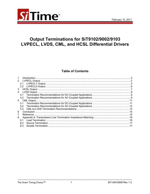
<strong>Output</strong> <strong>Terminations</strong> for SiT9102/9002/9103<strong>LVPECL</strong>, <strong>LVDS</strong>, CML, and <strong>HCSL</strong> differential drivers1 Introduction<strong>SiTime</strong> offers a wide selection of output differential signaling types to facilitate various clockapplications. The supported signaling types are <strong>LVPECL</strong> (Low-Voltage Positive Emitter-CoupledLogic), <strong>LVDS</strong> (Low-Voltage <strong>Differential</strong> Signaling), CML (Current Mode Logic), and <strong>HCSL</strong> (High-Speed Current Steering Logic).<strong>Differential</strong> signals typically have fast rise times, e.g., between 100ps and 400ps, which causeseven short traces to behave as transmission lines. These traces have to be terminated properlyfor minimal reflections, optimal signal integrity, and the least EMI.The traces in most high-speed differential applications are designed either as two 50Ωuncoupled transmission lines (each 50Ω to GND plane), or as one 100Ω coupled differentialtrace pair.Minimal reflections are achieved when the traces are terminated on one or both ends withimpedances that match the trace impedance. (Refer to Appendix A for more details aboutsource and/or load termination strategies.) In addition to impedance matching, the terminationnetworks impact the DC bias and AC voltage swings at the receivers. This application notedescribes each output type and the recommended termination methods for proper impedancematching, DC biasing, and AC swing levels.2 <strong>LVPECL</strong> <strong>Output</strong>The <strong>SiTime</strong> <strong>LVPECL</strong> outputs use current-mode drivers, primarily to accommodate multiplesignaling formats. Two types of <strong>LVPECL</strong> outputs are provided, “<strong>LVPECL</strong>0” and “<strong>LVPECL</strong>1”,each suitable for different set of termination methodologies that are either commonly used orwould provide specific benefits in some custom applications. <strong>SiTime</strong> generally recommends<strong>LVPECL</strong>0 and <strong>LVPECL</strong>1 as below:1. <strong>LVPECL</strong>0: when the device outputs are AC-coupled to the load termination circuit2. <strong>LVPECL</strong>1: when the device outputs are DC-coupled to the load termination circuit.The uses of <strong>LVPECL</strong>0 and <strong>LVPECL</strong>1 are not restricted to the two cases just listed. They mayalso be used in special applications, such as double termination. The following sections providefurther detail about using <strong>LVPECL</strong>0 and <strong>LVPECL</strong>1 outputs and the associated terminationrecommendations.--------------------------------------------------------------------------------------------------------------------------------------------The Smart Timing Choice 2 SiT-AN10009 Rev 1.3
<strong>Output</strong> <strong>Terminations</strong> for SiT9102/9002/9103<strong>LVPECL</strong>, <strong>LVDS</strong>, CML, and <strong>HCSL</strong> differential drivers2.1 <strong>LVPECL</strong>1 <strong>Output</strong>I CNISWICPFigure 1: <strong>SiTime</strong> <strong>LVPECL</strong>1 driver output structureThe structure of the <strong>SiTime</strong> <strong>LVPECL</strong>1 driver is shown in Figure 1. Each output is driven by twocurrent sources: a switched 16 mA current source ( ISW) and a dedicated constant 6 mA currentsource ( I CPor ICN). Typically, the outputs are terminated to VDD-2V via 50Ω resistors. Whenan output is high, it will source 22 mA of current (16 mA + 6 mA). When it is low, it will driveonly 6 mA of current. Consequently, the voltage developed across the 50Ω load resistor willvary nominally between 1.1V and 300 mV, thus creating a single-ended signal swing of 800mV.This single-ended signal swing is only nominally 800mV. Since the output voltage is proportionalto the value of the load resistor, large variations in resistor value may result in excessivevariations in voltage swing. For systems sensitive to signal swings beyond the nominal range,the use of 1% precision resistors is recommended.Figure 2 shows the typical termination network for DC-coupled load terminated <strong>LVPECL</strong>outputs. The outputs are terminated with a 50Ω resistor to the termination voltage (VT),providing good impedance match to the transmission line. In Figure 2, the receiver inputimpedance is assumed to be high (greater than 1kohm or so). Therefore, the 50Ω resistorsshould be placed as close to the receiver as possible to avoid the formation of unterminatedstubs, which can cause signal integrity issues. Note that the receiver may be connected in twoways: either directly to the termination circuit, or through AC-coupled capacitors. The latter isused when the receiver biasing is different from what the termination circuit provides.Figure 2: <strong>LVPECL</strong> with DC-coupled parallel Shunt load termination--------------------------------------------------------------------------------------------------------------------------------------------The Smart Timing Choice 3 SiT-AN10009 Rev 1.3
<strong>Output</strong> <strong>Terminations</strong> for SiT9102/9002/9103<strong>LVPECL</strong>, <strong>LVDS</strong>, CML, and <strong>HCSL</strong> differential driversFor <strong>SiTime</strong> <strong>LVPECL</strong> current drivers, output impedance is in the range of several K-ohms whileZ o is close to 50Ω for most traces and cables. This results in a source reflection coefficient ( ΓS)close to 100% (see Appendix A), thus reflecting back virtually all of the signal that has beenreflected from the load. Fortunately, the round-trip reflection signal is small because themajority of the signals will be absorbed by the load due to its low reflection coefficient ( Γ ).In applications where a separate termination voltage is not readily available, pull-up and pulldownresistors forming a Thevenin Equivalent network can terminate the 50Ω transmission line.Such a network effectively establishes a 50Ω impedance to the termination voltage of VDD-2Vat the receiver. This termination method is shown in Figure 3; note that the resistor values aredifferent for 3.3V and 2.5V supply voltages. As in Shunt load termination, the AC-coupledcapacitors may used between the termination network and the receiver where needed.LFigure 3: LEVPECL DC-coupled load termination with Thevenin Equivalent networkOUT+<strong>LVPECL</strong>1Y-Bias TerminationnetworkZo = 50Ω0.1μFD+OUT-Zo = 50Ω0.1μFD-VDDR1R2R3R1R23.3 V2.5 V50 Ω50 Ω50 Ω50 Ω50 Ω18 ΩC10.1μFR3Figure 4: <strong>LVPECL</strong> with Y-Bias terminationIn most case the Thevenin Equivalent termination works well, but it can be sensitive to thepower supply noise if there is any significant mismatch between traces or between the resistornetworks on each side of the differential pair, or if the receiver is too sensitive to common-modenoise. Figure 4 shows the Y-Bias termination network, which provides an effective terminationvoltage of VDD-2V without requiring either connection to VDD or access to an additionaltermination voltage source. The termination voltage is generated by the sum of differential pair--------------------------------------------------------------------------------------------------------------------------------------------The Smart Timing Choice 4 SiT-AN10009 Rev 1.3
<strong>Output</strong> <strong>Terminations</strong> for SiT9102/9002/9103<strong>LVPECL</strong>, <strong>LVDS</strong>, CML, and <strong>HCSL</strong> differential driverscurrents passing through the R3. The capacitance C1 is used to create AC ground at thetermination voltage. As in previous cases, the AC-coupled capacitors may be used between thetermination network and the receiver where needed.Parallel load termination may not provide the best signal integrity for some <strong>LVPECL</strong>applications, including the following cases:1. When it is difficult to place the termination network close to the receiver, i.e., within 0.1into 0.3in from the receiver. In such cases, the traces connecting the termination networkto the receiver will appear as a stub and will degrade signal integrity at the receiverinputs.2. When there are large capacitive loads at the receiver inputs. Such capacitive loads willreduce the termination impedance when the fast edges of the signal reach the receiver,causing a large load reflection coefficient. This reflection will return to the load with littleattenuation after being reflected at the source. The rule of thumb is that the terminationmismatch becomes significant if 3.Tr/( π . CL) is less than 50Ω, where Tris the 20%-to-80% rise time, and CLis the load capacitance.In such scenarios, source termination is a better option, which can be implemented by placingany of the termination networks shown in Figure 2, Figure 3, and Figure 4 close to the driver.(Refer to Appendix A for general details on source termination.)Note: The termination networks in Figure 2, Figure 3, and Figure 4 cannot be used for sourcetermination with the low-impedance <strong>LVPECL</strong> (open emitter) drivers. Such drivers require seriesimpedances for source termination (see Appendix A).For most applications, a single termination at the source or load minimizes the reflectionssufficiently. In some situations, it may not be possible to achieve good matching with load orsource termination alone. An effective strategy is double termination. Figure 5 shows anexample of double termination for <strong>LVPECL</strong> signals. Any combination of termination networksshown in Figure 2, Figure 3, and Figure 4 can be used at the source and load with <strong>SiTime</strong>LVEPCL outputs. When using Y-Bias termination in double termination cases, the R3 should be100Ω and 36Ω for 3.3V and 2.5V power supply voltages, respectively.Figure 5: <strong>LVPECL</strong> double termination (source and load)With the addition of the 50Ω termination at the source, a 25Ω equivalent load is presented to the<strong>LVPECL</strong> driver, reducing the differential signal swing from 1600 mV to 800 mV. If this signallevel is insufficient for the receiver, the user can choose the <strong>LVPECL</strong>0 version of the oscillatorwith higher switched current drivers. The switched current sources (see Figure 1) in these--------------------------------------------------------------------------------------------------------------------------------------------The Smart Timing Choice 5 SiT-AN10009 Rev 1.3
<strong>Output</strong> <strong>Terminations</strong> for SiT9102/9002/9103<strong>LVPECL</strong>, <strong>LVDS</strong>, CML, and <strong>HCSL</strong> differential driversoscillators are enhanced from 16 mA to 22 mA, thus increasing the signal swing for a 25Ω loadfrom 400 mV to 550 mV.2.2 <strong>LVPECL</strong>0 <strong>Output</strong>VDDChipboundaryI SW= 22mAOUT+OUT-Figure 6: <strong>LVPECL</strong>0 driver output structureThe <strong>LVPECL</strong>0 driver output structure is shown in Figure 6. The <strong>LVPECL</strong>0 switched current,ISW, is 22mA. This effectively increases the outputs’ switching drive capacity from the<strong>LVPECL</strong>1 mode’s 16mA to 22mA. One use of this mode is for <strong>LVPECL</strong> with an AC-coupledtermination circuit, as described below.An AC-coupled termination is often recommended when the <strong>LVPECL</strong> output drives a differentialreceiver with a termination voltage different from what the driver needs. As shown in Figure 7, acapacitor is used to block the DC path to the load termination and receiver, allowing the receiverto set its own termination voltage. In this example, the receiver inputs are biased by a 50Ωresistor to a termination voltage, which is determined by the receiver requirements. Since thecapacitor blocks the DC path for the driver’s outputs, additional 150Ω resistors are installedbetween the outputs and ground at the source to provide the required output DC current paths.From the AC standpoint, the R1/R2 resistors at the source are in parallel with the 50Ω resistorsat the load, resulting in a 37.5Ω equivalent load to the driver. To obtain the nominal <strong>LVPECL</strong>signal swings at the load, the user should choose the <strong>LVPECL</strong>0 output mode of SiT9102 with 22mA current drivers, thus increasing the nominal signal swing to 825 mV.Figure 7: <strong>LVPECL</strong>0 in load terminated AC-coupled application--------------------------------------------------------------------------------------------------------------------------------------------The Smart Timing Choice 6 SiT-AN10009 Rev 1.3
<strong>Output</strong> <strong>Terminations</strong> for SiT9102/9002/9103<strong>LVPECL</strong>, <strong>LVDS</strong>, CML, and <strong>HCSL</strong> differential drivers3 <strong>HCSL</strong> <strong>Output</strong>VDDI SW= 15mAChipboundaryOUT+OUT-Figure 8: <strong>HCSL</strong> driver output structureThe <strong>HCSL</strong> output structure (see Figure 8) is driven by a 15 mA switched current source typicallyterminated to ground via a 50Ω resistor. The nominal signal swing is 750 mV. The <strong>HCSL</strong>interface is typically source-terminated with a 50Ω load as shown in Figure 9. The open-draintransistor at the output has fairly high impedance in the range of several kilo-ohms. From an ACstandard point, the output transistor’s impedance is parallel to the 50Ω load resistor, resulting inan equivalent resistance very close to 50Ω. Since the traces used in this interface have acharacteristic impedance of 50Ω, any signal reflected from the load will be absorbed at thesource. Typically, two small resistors, R1 and R2 (see Figure 9), are placed in series with thehigh-impedance driver. They function as an overshoot limiter by slowing down the rapid rise ofcurrent from the output, and have no impact on the impedance matching at the source. <strong>SiTime</strong>recommends 20Ω for these resistors.Figure 9: <strong>HCSL</strong> interface termination--------------------------------------------------------------------------------------------------------------------------------------------The Smart Timing Choice 7 SiT-AN10009 Rev 1.3
<strong>Output</strong> <strong>Terminations</strong> for SiT9102/9002/9103<strong>LVPECL</strong>, <strong>LVDS</strong>, CML, and <strong>HCSL</strong> differential drivers4 <strong>LVDS</strong> <strong>Output</strong>VDDI SWChipboundaryIN-CAIN+OUT+OUT-100ΩBDI SWSwing typeNormalHighI SW3.5 mA7 mAFigure 10: <strong>LVDS</strong> driver output structure<strong>LVDS</strong> [1] is a high-speed digital interface suitable for many applications that require low powerconsumption and high noise immunity. <strong>LVDS</strong> uses differential signals with low voltage swings totransmit data at high rates. Figure 10 shows the output structure of an <strong>LVDS</strong> driver, consistingof a 3.5 mA nominal current source connected to differential outputs via a switching network.The outputs are typically attached to 100Ω differential transmission lines terminated with a 100Ωresistor at the receiver end. The resistor’s impedance matches the impedance of thetransmission lines and provides a current path for the signal. The common mode voltage isspecified at 1.2V.Signal switching is accomplished with four transistors labeled A, B, C, and D, respectively.Because the impedance of the receiver is typically high, virtually all of the current from the driverwill flow through the 100Ω resistor, resulting in a voltage difference of 350 mV between thereceiver inputs. In Figure 10, when the signal IN is low, transistors A and B will be turned on;the current will flow through transistor A and the 100Ω resistor, and return through transistor B.When signal IN is high, transistors C and D will be turned on; the current will flow throughtransistor C and the 100Ω resistor, and return through transistor D, resulting in -350mV voltageacross the receiver.For the receiver, the direction of the current flowing through the termination resistor determineswhether a positive or negative differential voltage is registered. A positive differential voltagerepresents a logic high level, while a negative differential voltage represents a logic low level.<strong>SiTime</strong> provides two types of <strong>LVDS</strong> output swings: normal and high. The “normal swing”version has a 3.5 mA current source while the “high swing” version features a 7 mA currentsource. The high swing version is designed to be used in double termination configurations.Both versions are available for 3.3V and 2.5V applications.--------------------------------------------------------------------------------------------------------------------------------------------The Smart Timing Choice 8 SiT-AN10009 Rev 1.3
<strong>Output</strong> <strong>Terminations</strong> for SiT9102/9002/9103<strong>LVPECL</strong>, <strong>LVDS</strong>, CML, and <strong>HCSL</strong> differential drivers4.1 Termination Recommendations for DC-Coupled ApplicationsA <strong>LVDS</strong> interface with 100Ω differential traces is typically terminated at the receiver end with a100Ω resistor across the differential inputs of the receiver (see Figure 11). Some receivershave incorporated the 100Ω resistor on-chip, eliminating the need for external termination.OUT+Zo = 50ΩZo = 50Ω100 ΩOUT+OUT-OUT-<strong>LVDS</strong>, Normal swingFigure 11: <strong>LVDS</strong> single DC termination at the loadFor most applications, a single termination at the load is sufficient. In situations where the loadreflection coefficient is relatively high, a double termination arrangement may reduce the overallround trip (see Figure 12). (Refer to Appendix A for more information on the uses of single anddouble termination arrangements.) With a 100Ω resistor at both the source and the load, theequivalent resistance at the output driver is reduced to 50Ω, causing the output signal swing tobe cut in half. <strong>SiTime</strong> provides the high swing option for its <strong>LVDS</strong> drivers with 7 mA currentdrive to restore the differential signal swing to ±350 mV.OUT+100 ΩZo = 50ΩZo = 50Ω100 ΩOUT+OUT-OUT-<strong>LVDS</strong>, High swingFigure 12: <strong>LVDS</strong> double DC termination4.2 Termination Recommendations for AC-Coupled ApplicationsIf the <strong>LVDS</strong> driver and the receiver are operating with different common mode voltages, then anAC termination is recommended. A capacitor is used to block the DC current path from thedriver; in such cases, the receiver must implement its own input bias circuit.AC coupling can be configured as either a single termination at the load or as a doubletermination. With a single load termination, as shown in Figure 13, the AC-coupled capacitorsshould be placed between termination resistor and the receiver for proper DC biasing of thedriver. For double-terminated links, the AC-coupling capacitor can be placed before (Figure 14)or after (Figure 15) the load termination resistor. The high swing version may be used with thedouble termination.--------------------------------------------------------------------------------------------------------------------------------------------The Smart Timing Choice 9 SiT-AN10009 Rev 1.3
<strong>Output</strong> <strong>Terminations</strong> for SiT9102/9002/9103<strong>LVPECL</strong>, <strong>LVDS</strong>, CML, and <strong>HCSL</strong> differential driversOUT+Zo = 50ΩZo = 50Ω100 Ω0.1μF0.1μFOUT+OUT-OUT-<strong>LVDS</strong>, Normal swingFigure 13: <strong>LVDS</strong> single AC termination at the loadThe double terminations shown in Figure 14 and Figure 15 differ only in the position of the ACcouplingcapacitor. The capacitor in Figure 14 is charged by the common mode current flowingthrough half the differential resistance, which is the equivalent of 50Ω. On the other hand, thecapacitor in Figure 15 is charged by the current through the resistance of the receiver’s inputs,which can be in the range of kilo-ohms. During clock start-up, the capacitor shown in Figure 14will be charged much faster than that shown in Figure 15. Therefore, a valid clock signal will beavailable sooner to the receiver. If fast clock start-up is important, the configuration shown inFigure 14 is preferable.OUT+100 Ω0.1μF0.1μFZo = 50ΩZo = 50Ω100 ΩOUT+OUT-OUT-<strong>LVDS</strong>, High swingFigure 14: <strong>LVDS</strong> double AC termination with capacitor close to the sourceIn data transmission applications, the configuration shown in Figure 15 may be moreadvantageous. Because of its higher RC time constant, it can sustain data sequences withlonger 1s and 0s without experiencing significant voltage droop.OUT+100 ΩZo = 50ΩZo = 50Ω100 Ω0.1μF0.1μFOUT+OUT-OUT-<strong>LVDS</strong>, Normal swingFigure 15: <strong>LVDS</strong> double AC termination with capacitor close to the load--------------------------------------------------------------------------------------------------------------------------------------------The Smart Timing Choice 10 SiT-AN10009 Rev 1.3
<strong>Output</strong> <strong>Terminations</strong> for SiT9102/9002/9103<strong>LVPECL</strong>, <strong>LVDS</strong>, CML, and <strong>HCSL</strong> differential drivers5 CML <strong>Output</strong>OUT+OUT-ChipboundaryI SWSwing typeNormalHighI SW8 mA16 mAFigure 16: CML driver output structure<strong>SiTime</strong> CML drivers are constructed with an NMOS open-drain differential pair and an 8 mAconstant current source. The output structure is shown in Figure 16. Because the open-draintransistors are only capable of pulling down a signal, external pull-up resistors are needed.Voltage swing across a 50Ω resistor is typically 400 mV.<strong>SiTime</strong>’s CML clocks can operate at 3.3V, 2.5V, and 1.8V. Two output signal swing versionsare supported: normal and high. The normal swing version is equipped with an 8 mA currentsource, while the high swing version has a 16 mA current source.5.1 Termination Recommendations for DC-Coupled ApplicationsFigure 17: CML with single DC load terminationA typical CML termination is shown in Figure 17. The differential outputs are pulled up to atermination voltage. In most cases, the driver supply voltage (VDD DR ) is used for the VT.However, in applications where the driver and the receiver are operated at different VDDs, VT istypically set to the driver supply voltage or the higher of the two VDDs, as long as it does notexceed the maximum allowable voltage for the driver or the receiver.For a double termination strategy, both the source and the load are typically terminated to thesame VT, as shown in Figure 18. Because two 50Ω termination resistors are connected inparallel to the output, their equivalent resistance is reduced to 25Ω, causing a 50% reduction inthe output swing. <strong>SiTime</strong> offers the CML high swing version with 16 mA current drivers torestore the signal swing back to 400mV.--------------------------------------------------------------------------------------------------------------------------------------------The Smart Timing Choice 11 SiT-AN10009 Rev 1.3
<strong>Output</strong> <strong>Terminations</strong> for SiT9102/9002/9103<strong>LVPECL</strong>, <strong>LVDS</strong>, CML, and <strong>HCSL</strong> differential driversFigure 18: CML with double DC termination5.2 Termination Recommendations for AC-Coupled ApplicationsAC termination should be used if the receiver requires a different input bias from what thetermination provides. The DC path to the receiver is blocked by the capacitor, so the user mustprovide a separate bias circuit for the receiver inputs. In many cases, a single termination at theload end is sufficient (see Figure 18). The VT is typically the VDD of the driver.Figure 19: CML single AC termination at the loadFor better signal integrity, double termination configurations, shown in Figure 20 and Figure 21,may be used. The CML high swing version may be used in double terminations to maintain a400 mV signal swing. As in the discussion about AC coupling with <strong>LVDS</strong> links, the maindifference between the AC coupling shown in Figure 20 and Figure 21 is the effective timeconstant for the common-mode signal. The first provides shorter time constants, which may beadvantageous for getting stable signals faster in clock applications. The longer time constantsshown in Figure 21 may be preferable in data-carrying links, to sustain data sequences withlonger 1s and 0s without experiencing significant voltage droop.--------------------------------------------------------------------------------------------------------------------------------------------The Smart Timing Choice 12 SiT-AN10009 Rev 1.3
<strong>Output</strong> <strong>Terminations</strong> for SiT9102/9002/9103<strong>LVPECL</strong>, <strong>LVDS</strong>, CML, and <strong>HCSL</strong> differential driverswhere I DC= 8mArepresents the DC current going through the termination circuit (R1||R2). Areasonable choice is to remove R2, i.e., R 2 = ∞ , which leads to the following values for R1:• VDD=3.3V R1=225Ω, 1%• VDD=2.5V R1=125Ω, 1%• VDD=1.8V R1=37.5Ω, 1%VDDR1VT0.1μFR2VDD50 Ω50 ΩVDDOUT+Zo = 50ΩD+OUT-Zo = 50ΩD-CML driver withNormal swingFigure 22: CML-to-<strong>LVDS</strong> Shunt termination networkAnother method for connecting CML outputs to <strong>LVDS</strong> inputs is to decouple the DC levels usingAC-coupling capacitors, as shown in Figure 23. The bias circuits, R1=R3 and R2=R4, should bedesigned to provide the <strong>LVDS</strong> offset voltage of 1.25V at the receiver. The termination resistors,AC-coupled capacitors, and the bias networks should be placed close to the receiver for bestsignal integrity. From an AC point of view, the bias network impedance is in parallel with thetermination resistor. To avoid significant mismatch due to the bias networks, the R1||R2 shouldbe great than 1kΩ.Figure 23: CML-to-<strong>LVDS</strong> interface with AC coupling and DC bias circuitThe AC coupling method shown in Figure 23 may also be used to interface CML outputs to<strong>LVPECL</strong> inputs provided that the bias networks are designed for the nominal offset of <strong>LVPECL</strong>circuits, which is typically VDD-1.3V.--------------------------------------------------------------------------------------------------------------------------------------------The Smart Timing Choice 14 SiT-AN10009 Rev 1.3
<strong>Output</strong> <strong>Terminations</strong> for SiT9102/9002/9103<strong>LVPECL</strong>, <strong>LVDS</strong>, CML, and <strong>HCSL</strong> differential drivers6 ConclusionThis application note presented the SiT9102, SiT9002, and SiT9103 differential output driverstructures and the most commonly used AC-coupled and DC-coupled terminationrecommendations for four types of differential outputs: <strong>LVPECL</strong>, <strong>HCSL</strong>, <strong>LVDS</strong>, and CML.Additionally, multiple current strength options in these clocks support double terminationstrategies without sacrificing signal swing voltages. With such a rich selection of output types,users can easily find the ones that fit their design requirements.7 Reference[1] Telecommunications Industry Association, “Electrical Characteristics of low voltagedifferential signaling (<strong>LVDS</strong>) interface circuits”, TIA/EIA-644-A standard specifications,February 2001.--------------------------------------------------------------------------------------------------------------------------------------------The Smart Timing Choice 15 SiT-AN10009 Rev 1.3
<strong>Output</strong> <strong>Terminations</strong> for SiT9102/9002/9103<strong>LVPECL</strong>, <strong>LVDS</strong>, CML, and <strong>HCSL</strong> differential drivers8 Appendix A: Transmission Line Termination ImpedanceMatchingAny trace of a printed circuit board (PCB) or cable behaves as a transmission line when itselectrical length is greater than half of the 20%-to-80% rise time of the signal that is beinglaunched to the trace. Proper termination is an important factor for optimal signal integrity. ThisAppendix discusses source, load, and double termination strategies.8.1 Load TerminationZoZoV + -ReceiverZ LIReceiverZ L(a)(b)Figure 24: Transmission line parallel load terminationFigure 24 (a) and (b) show transmission lines terminated with parallel load impedance of ZLand driven by a voltage or current signal. Once the signal reaches the load at the other side ofthe line, some of its energy will be absorbed by the load and the rest will reflect back to thesource. The ratio of the reflected signal to the incident one is referred to as the reflectioncoefficient and is computed as below:ZL− ZoΓL=Equation 2ZL+ ZoIf the load is terminated with the same impedance as the trace, i.e., ZL= Zo, then Γ L= 0 ,which means no signal will reflect back. If the load impedance does not match that of the trace,some of the signal will reflect to the source. A fraction of the reflected signal will reflect back tothe load depending on the source reflection coefficient, computed as below:Z− ZS oΓS=Equation 3ZS+ ZoThe overall reflection seen at the load is the result of round-trip reflection through thetransmission line, which can be computed using the round-trip reflection coefficient, Γ RT,computed as below:Γ = Γ . ΓEquation 4RTSLThe round-trip reflection Γ RTshould be minimized for optimal signal integrity. A large value ofΓRTcan cause reduced signal margin, extra trigger edges in digital applications, or excessiveringing at load.--------------------------------------------------------------------------------------------------------------------------------------------The Smart Timing Choice 16 SiT-AN10009 Rev 1.3
<strong>Output</strong> <strong>Terminations</strong> for SiT9102/9002/9103<strong>LVPECL</strong>, <strong>LVDS</strong>, CML, and <strong>HCSL</strong> differential driversFor the voltage driver in Figure 24(a), ZS= 0 , which leads to Γ S= −1, while for the currentdriver in Figure 24(b), ZS= ∞ , which leads to Γ S= + 1. In both cases, all the energy of thesignal reflected from the load will reflect back to the load, leading to ΓRT= −ΓLand ΓRT= ΓLforFigure 24(a) and Figure 24(b), respectively. Therefore, the load impedance should be matchedwell with that of the trace to avoid signal integrity issues.8.2 Source TerminationZ SZoZoV + -Z SReceiverIZ SZ SReceiver(a)(b)Figure 25: Transmission line source terminationIn some applications, it is difficult to properly terminate the transmission line at the load, forexample, due to uncontrolled impedances at the load or inability to place the termination closeto the receiver circuit at the end of the line. In such cases, the source termination strategiesshown in Figure 25(a) and (b) can be used. The receivers are assumed to have highimpedance, which leads to a load reflection coefficient of 1 ( Γ L= + 1). The signal will reflect tothe source, where much of the energy gets absorbed by the source impedance when Z Sismatched to Zo, and only a small portion will reflect back to the load. The round-trip reflectioncoefficient will be Γ = Γ .RT8.3 Double TerminationSZ SZoZoV + -Z SReceiverZ LIZ SZ SReceiverZ L(a)(b)Figure 26: Double termination techniqueIn some applications it may be difficult to reduce load or source reflection coefficients toacceptably small values, e.g., due to the excessive parasitic capacitances and inductances.Terminating at both ends of the transmission line is an effective way to reduce round-tripreflection and improve signal integrity. Figure 26 shows double termination for voltage andcurrent drivers. For example, if ΓL = ΓS= 0. 1, then Γ RT= 0. 01, i.e., only 1% of the signal reflectback to the load.--------------------------------------------------------------------------------------------------------------------------------------------The Smart Timing Choice 17 SiT-AN10009 Rev 1.3
<strong>Output</strong> <strong>Terminations</strong> for SiT9102/9002/9103<strong>LVPECL</strong>, <strong>LVDS</strong>, CML, and <strong>HCSL</strong> differential driversOne drawback of double termination is that the effective signal reaching the load will be half ofthe signal in load- or source-only terminated circuits. Drivers that can provide twice the nominaldrive are attractive solutions to signal integrity problems using the double termination strategy.The additional drive causes more power consumption in the load and source terminations, butoverall power consumption goes up only marginally in cases where the load power consumptionis small relative to that of the driver.<strong>SiTime</strong> Corporation990 Almanor AvenueSunnyvale, CA 94085USAPhone: 408-328-4400http://www.sitime.com© <strong>SiTime</strong> Corporation, 2008-2011. The information contained herein is subject to change at any time without notice. <strong>SiTime</strong>assumes no responsibility or liability for any loss, damage or defect of a Product which is caused in whole or in part by (i) use of anycircuitry other than circuitry embodied in a <strong>SiTime</strong> product, (ii) misuse or abuse including static discharge, neglect or accident, (iii)unauthorized modification or repairs which have been soldered or altered during assembly and are not capable of being tested by<strong>SiTime</strong> under its normal test conditions, or (iv) improper installation, storage, handling, warehousing or transportation, or (v) beingsubjected to unusual physical, thermal, or electrical stress.Disclaimer: <strong>SiTime</strong> makes no warranty of any kind, express or implied, with regard to this material, and specifically disclaims anyand all express or implied warranties, either in fact or by operation of law, statutory or otherwise, including the implied warranties ofmerchantability and fitness for use or a particular purpose, and any implied warranty arising from course of dealing or usage oftrade, as well as any common-law duties relating to accuracy or lack of negligence, with respect to this material, any <strong>SiTime</strong> productand any product documentation. Products sold by <strong>SiTime</strong> are not suitable or intended to be used in a life support application orcomponent, to operate nuclear facilities, or in other mission critical applications where human life may be involved or at stake.--------------------------------------------------------------------------------------------------------------------------------------------The Smart Timing Choice 18 SiT-AN10009 Rev 1.3


