Differential Output Terminations LVPECL, HCSL, LVDS ... - SiTime
Differential Output Terminations LVPECL, HCSL, LVDS ... - SiTime
Differential Output Terminations LVPECL, HCSL, LVDS ... - SiTime
- No tags were found...

You also want an ePaper? Increase the reach of your titles
YUMPU automatically turns print PDFs into web optimized ePapers that Google loves.
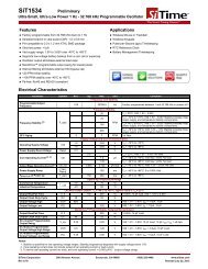
<strong>Output</strong> <strong>Terminations</strong> for SiT9102/9002/9103<strong>LVPECL</strong>, <strong>LVDS</strong>, CML, and <strong>HCSL</strong> differential drivers4 <strong>LVDS</strong> <strong>Output</strong>VDDI SWChipboundaryIN-CAIN+OUT+OUT-100ΩBDI SWSwing typeNormalHighI SW3.5 mA7 mAFigure 10: <strong>LVDS</strong> driver output structure<strong>LVDS</strong> [1] is a high-speed digital interface suitable for many applications that require low powerconsumption and high noise immunity. <strong>LVDS</strong> uses differential signals with low voltage swings totransmit data at high rates. Figure 10 shows the output structure of an <strong>LVDS</strong> driver, consistingof a 3.5 mA nominal current source connected to differential outputs via a switching network.The outputs are typically attached to 100Ω differential transmission lines terminated with a 100Ωresistor at the receiver end. The resistor’s impedance matches the impedance of thetransmission lines and provides a current path for the signal. The common mode voltage isspecified at 1.2V.Signal switching is accomplished with four transistors labeled A, B, C, and D, respectively.Because the impedance of the receiver is typically high, virtually all of the current from the driverwill flow through the 100Ω resistor, resulting in a voltage difference of 350 mV between thereceiver inputs. In Figure 10, when the signal IN is low, transistors A and B will be turned on;the current will flow through transistor A and the 100Ω resistor, and return through transistor B.When signal IN is high, transistors C and D will be turned on; the current will flow throughtransistor C and the 100Ω resistor, and return through transistor D, resulting in -350mV voltageacross the receiver.For the receiver, the direction of the current flowing through the termination resistor determineswhether a positive or negative differential voltage is registered. A positive differential voltagerepresents a logic high level, while a negative differential voltage represents a logic low level.<strong>SiTime</strong> provides two types of <strong>LVDS</strong> output swings: normal and high. The “normal swing”version has a 3.5 mA current source while the “high swing” version features a 7 mA currentsource. The high swing version is designed to be used in double termination configurations.Both versions are available for 3.3V and 2.5V applications.--------------------------------------------------------------------------------------------------------------------------------------------The Smart Timing Choice 8 SiT-AN10009 Rev 1.3