MCP1702 250 mA Low Quiescent Current LDO Regulator - Microchip
MCP1702 250 mA Low Quiescent Current LDO Regulator - Microchip
MCP1702 250 mA Low Quiescent Current LDO Regulator - Microchip

You also want an ePaper? Increase the reach of your titles
YUMPU automatically turns print PDFs into web optimized ePapers that Google loves.
<strong>MCP1702</strong><br />
<strong>250</strong> <strong>mA</strong> <strong>Low</strong> <strong>Quiescent</strong> <strong>Current</strong> <strong>LDO</strong> <strong>Regulator</strong><br />
Features:<br />
• 2.0 µA <strong>Quiescent</strong> <strong>Current</strong> (typical)<br />
• Input Operating Voltage Range: 2.7V to 13.2V<br />
• <strong>250</strong> <strong>mA</strong> Output <strong>Current</strong> for Output Voltages 2.5V<br />
• 200 <strong>mA</strong> Output <strong>Current</strong> for Output Voltages < 2.5V<br />
• <strong>Low</strong> Dropout (<strong>LDO</strong>) Voltage<br />
- 625 mV typical @ <strong>250</strong> <strong>mA</strong> (V OUT = 2.8V)<br />
• 0.4% Typical Output Voltage Tolerance<br />
• Standard Output Voltage Options:<br />
- 1.2V, 1.5V, 1.8V, 2.5V, 2.8V,<br />
3.0V, 3.3V, 4.0V, 5.0V<br />
• Output Voltage Range 1.2V to 5.5V in 0.1V<br />
Increments (50 mV increments available upon<br />
request)<br />
• Stable with 1.0 µF to 22 µF Output Capacitor<br />
• Short-Circuit Protection<br />
• Overtemperature Protection<br />
Applications:<br />
• Battery-powered Devices<br />
• Battery-powered Alarm Circuits<br />
• Smoke Detectors<br />
• CO 2 Detectors<br />
• Pagers and Cellular Phones<br />
• Smart Battery Packs<br />
• <strong>Low</strong> <strong>Quiescent</strong> <strong>Current</strong> Voltage Reference<br />
• PDAs<br />
• Digital Cameras<br />
• Microcontroller Power<br />
• Solar-Powered Instruments<br />
• Consumer Products<br />
• Battery Powered Data Loggers<br />
Related Literature:<br />
• AN765, “Using <strong>Microchip</strong>’s Micropower <strong>LDO</strong>s”,<br />
DS00765, <strong>Microchip</strong> Technology Inc., 2002<br />
• AN766, “Pin-Compatible CMOS Upgrades to<br />
Bipolar <strong>LDO</strong>s”, DS00766,<br />
<strong>Microchip</strong> Technology Inc., 2002<br />
• AN792, “A Method to Determine How Much<br />
Power a SOT-23 Can Dissipate in an Application”,<br />
DS00792, <strong>Microchip</strong> Technology Inc., 2001<br />
Description:<br />
The <strong>MCP1702</strong> is a family of CMOS low dropout (<strong>LDO</strong>)<br />
voltage regulators that can deliver up to <strong>250</strong> <strong>mA</strong> of<br />
current while consuming only 2.0 µA of quiescent<br />
current (typical). The input operating range is specified<br />
from 2.7V to 13.2V, making it an ideal choice for two to<br />
six primary cell battery-powered applications, 9V<br />
alkaline and one or two cell Li-Ion-powered<br />
applications.<br />
The <strong>MCP1702</strong> is capable of delivering <strong>250</strong> <strong>mA</strong> with<br />
only 625 mV (typical) of input to output voltage<br />
differential (V OUT = 2.8V). The output voltage tolerance<br />
of the <strong>MCP1702</strong> is typically ±0.4% at +25°C and ±3%<br />
maximum over the operating junction temperature<br />
range of -40°C to +125°C. Line regulation is ±0.1%<br />
typical at +25°C.<br />
Output voltages available for the <strong>MCP1702</strong> range from<br />
1.2V to 5.0V. The <strong>LDO</strong> output is stable when using only<br />
1 µF of output capacitance. Ceramic, tantalum or<br />
aluminum electrolytic capacitors can all be used for<br />
input and output. Overcurrent limit and<br />
overtemperature shutdown provide a robust solution<br />
for any application.<br />
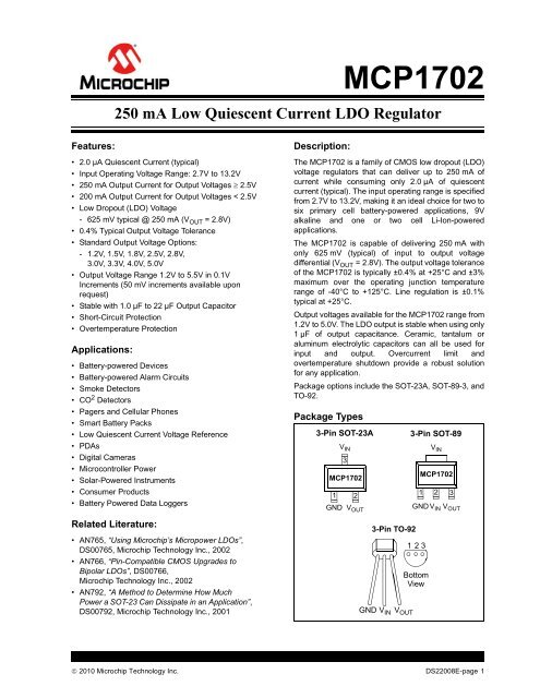
Package options include the SOT-23A, SOT-89-3, and<br />
TO-92.<br />
Package Types<br />
3-Pin SOT-23A<br />
1<br />
V IN<br />
3<br />
<strong>MCP1702</strong><br />
2<br />
GND V OUT<br />
3-Pin TO-92<br />
GND V IN V OUT<br />
3-Pin SOT-89<br />
V IN<br />
<strong>MCP1702</strong><br />
1 2 3<br />
GND V IN V OUT<br />
123<br />
Bottom<br />
View<br />
2010 <strong>Microchip</strong> Technology Inc. DS22008E-page 1
<strong>MCP1702</strong><br />
Functional Block Diagrams<br />
<strong>MCP1702</strong><br />
V IN<br />
V OUT<br />
Error Amplifier<br />
Voltage<br />
Reference<br />
-<br />
+<br />
+V IN<br />
Overcurrent<br />
Overtemperature<br />
GND<br />
Typical Application Circuits<br />
9V<br />
Battery<br />
+<br />
C IN<br />
1µF Ceramic<br />
<strong>MCP1702</strong><br />
V OUT<br />
3.3V<br />
V OUT<br />
V IN I OUT<br />
V IN<br />
C OUT 50 <strong>mA</strong><br />
1µF Ceramic<br />
GND<br />
DS22008E-page 2<br />
2010 <strong>Microchip</strong> Technology Inc.
<strong>MCP1702</strong><br />
1.0 ELECTRICAL<br />
CHARACTERISTICS<br />
Absolute Maximum Ratings †<br />
V DD ...............................................................................+14.5V<br />
All inputs and outputs w.r.t. .............(V SS -0.3V) to (V IN +0.3V)<br />
Peak Output <strong>Current</strong> ...................................................500 <strong>mA</strong><br />
Storage temperature .....................................-65°C to +150°C<br />
Maximum Junction Temperature................................... 150°C<br />
ESD protection on all pins (HBM;MM) 4 kV; 400V<br />
DC CHARACTERISTICS<br />
† Notice: Stresses above those listed under “Maximum<br />
Ratings” may cause permanent damage to the device. This is<br />
a stress rating only and functional operation of the device at<br />
those or any other conditions above those indicated in the<br />
operational listings of this specification is not implied.<br />
Exposure to maximum rating conditions for extended periods<br />
may affect device reliability.<br />
Electrical Specifications: Unless otherwise specified, all limits are established for V IN = V OUT(MAX) + V DROPOUT(MAX) , Note 1,<br />
I LOAD = 100 µA, C OUT = 1 µF (X7R), C IN = 1 µF (X7R), T A = +25°C.<br />
Boldface type applies for junction temperatures, T J of -40°C to +125°C. (Note 7)<br />
Parameters Sym Min Typ Max Units Conditions<br />
Input / Output Characteristics<br />
Input Operating Voltage V IN 2.7 — 13.2 V Note 1<br />
Input <strong>Quiescent</strong> <strong>Current</strong> I q — 2.0 5 µA I L = 0 <strong>mA</strong><br />
Maximum Output <strong>Current</strong> I OUT_<strong>mA</strong> <strong>250</strong> — — <strong>mA</strong> For V R 2.5V<br />
50 100 — <strong>mA</strong> For V R < 2.5V, V IN 2.7V<br />
100 130 — <strong>mA</strong> For V R < 2.5V, V IN 2.95V<br />
150 200 — <strong>mA</strong> For V R < 2.5V, V IN 3.2V<br />
200 <strong>250</strong> — <strong>mA</strong> For V R < 2.5V, V IN 3.45V<br />
Output Short Circuit <strong>Current</strong> I OUT_SC — 400 — <strong>mA</strong> V IN = V IN(MIN) (Note 1), V OUT = GND,<br />
<strong>Current</strong> (average current) measured<br />
10 ms after short is applied.<br />
Output Voltage Regulation V OUT V R -3.0% V R ±0.4% V R +3.0% V Note 2<br />
V R -2.0% V R ±0.4% V R +2.0% V<br />
V R -1.0% V R ±0.4% V R +1.0% V 1% Custom<br />
V OUT Temperature<br />
Coefficient<br />
TCV OUT — 50 — ppm/°C Note 3<br />
Line Regulation V OUT /<br />
(V OUT XV IN )<br />
-0.3 ±0.1 +0.3 %/V (V OUT(MAX) + V DROPOUT(MAX) )<br />
V IN 13.2V, (Note 1)<br />
Load Regulation V OUT /V OUT -2.5 ±1.0 +2.5 % I L = 1.0 <strong>mA</strong> to <strong>250</strong> <strong>mA</strong> for V R 2.5V<br />
I L = 1.0 <strong>mA</strong> to 200 <strong>mA</strong> for V R 2.5V,<br />
V IN = 3.45V (Note 4)<br />
Note 1: The minimum V IN must meet two conditions: V IN 2.7V and V IN V OUT(MAX) + V DROPOUT(MAX) .<br />
2: V R is the nominal regulator output voltage. For example: V R = 1.2V, 1.5V, 1.8V, 2.5V, 2.8V, 3.0V, 3.3V, 4.0V, or 5.0V. The<br />
input voltage V IN = V OUT(MAX) + V DROPOUT(MAX) or V IN = 2.7V (whichever is greater); I OUT = 100 µA.<br />
3: TCV OUT = (V OUT-HIGH - V OUT-LOW ) *10 6 / (V R * Temperature), V OUT-HIGH = highest voltage measured over the<br />
temperature range. V OUT-LOW = lowest voltage measured over the temperature range.<br />
4: Load regulation is measured at a constant junction temperature using low duty cycle pulse testing. Changes in output<br />
voltage due to heating effects are determined using thermal regulation specification TCV OUT .<br />
5: Dropout voltage is defined as the input to output differential at which the output voltage drops 2% below its measured<br />
value with an applied input voltage of V OUT(MAX) + V DROPOUT(MAX) or 2.7V, whichever is greater.<br />
6: The maximum allowable power dissipation is a function of ambient temperature, the maximum allowable junction<br />
temperature and the thermal resistance from junction to air (i.e., T A , T J , JA ). Exceeding the maximum allowable power<br />
dissipation will cause the device operating junction temperature to exceed the maximum 150°C rating. Sustained<br />
junction temperatures above 150°C can impact the device reliability.<br />
7: The junction temperature is approximated by soaking the device under test at an ambient temperature equal to the<br />
desired Junction temperature. The test time is small enough such that the rise in the Junction temperature over the<br />
ambient temperature is not significant.<br />
2010 <strong>Microchip</strong> Technology Inc. DS22008E-page 3
<strong>MCP1702</strong><br />
DC CHARACTERISTICS (CONTINUED)<br />
Electrical Specifications: Unless otherwise specified, all limits are established for V IN = V OUT(MAX) + V DROPOUT(MAX) , Note 1,<br />
I LOAD = 100 µA, C OUT = 1 µF (X7R), C IN = 1 µF (X7R), T A = +25°C.<br />
Boldface type applies for junction temperatures, T J of -40°C to +125°C. (Note 7)<br />
Parameters Sym Min Typ Max Units Conditions<br />
Dropout Voltage<br />
(Note 1, Note 5)<br />
V DROPOUT — 330 650 mV I L = <strong>250</strong> <strong>mA</strong>, V R = 5.0V<br />
— 525 725 mV I L = <strong>250</strong> <strong>mA</strong>, 3.3V V R < 5.0V<br />
— 625 975 mV I L = <strong>250</strong> <strong>mA</strong>, 2.8V V R < 3.3V<br />
— 750 1100 mV I L = <strong>250</strong> <strong>mA</strong>, 2.5V V R < 2.8V<br />
— — — mV V R < 2.5V, See Maximum Output<br />
<strong>Current</strong> Parameter<br />
Output Delay Time T DELAY — 1000 — µs V IN = 0V to 6V, V OUT = 90% V R<br />
R L = 50 resistive<br />
Output Noise e N — 8 — µV/(Hz) 1/2 I L = 50 <strong>mA</strong>, f = 1 kHz, C OUT = 1 µF<br />
Power Supply Ripple<br />
Rejection Ratio<br />
PSRR — 44 — dB f = 100 Hz, C OUT = 1 µF, I L = 50 <strong>mA</strong>,<br />
V INAC = 100 mV pk-pk, C IN = 0 µF,<br />
V R =1.2V<br />
Thermal Shutdown<br />
Protection<br />
T SD — 150 — °C<br />
Note 1: The minimum V IN must meet two conditions: V IN 2.7V and V IN V OUT(MAX) + V DROPOUT(MAX) .<br />
2: V R is the nominal regulator output voltage. For example: V R = 1.2V, 1.5V, 1.8V, 2.5V, 2.8V, 3.0V, 3.3V, 4.0V, or 5.0V. The<br />
input voltage V IN = V OUT(MAX) + V DROPOUT(MAX) or V IN = 2.7V (whichever is greater); I OUT = 100 µA.<br />
3: TCV OUT = (V OUT-HIGH - V OUT-LOW ) *10 6 / (V R * Temperature), V OUT-HIGH = highest voltage measured over the<br />
temperature range. V OUT-LOW = lowest voltage measured over the temperature range.<br />
4: Load regulation is measured at a constant junction temperature using low duty cycle pulse testing. Changes in output<br />
voltage due to heating effects are determined using thermal regulation specification TCV OUT .<br />
5: Dropout voltage is defined as the input to output differential at which the output voltage drops 2% below its measured<br />
value with an applied input voltage of V OUT(MAX) + V DROPOUT(MAX) or 2.7V, whichever is greater.<br />
6: The maximum allowable power dissipation is a function of ambient temperature, the maximum allowable junction<br />
temperature and the thermal resistance from junction to air (i.e., T A , T J , JA ). Exceeding the maximum allowable power<br />
dissipation will cause the device operating junction temperature to exceed the maximum 150°C rating. Sustained<br />
junction temperatures above 150°C can impact the device reliability.<br />
7: The junction temperature is approximated by soaking the device under test at an ambient temperature equal to the<br />
desired Junction temperature. The test time is small enough such that the rise in the Junction temperature over the<br />
ambient temperature is not significant.<br />
DS22008E-page 4<br />
2010 <strong>Microchip</strong> Technology Inc.
<strong>MCP1702</strong><br />
TEMPERATURE SPECIFICATIONS (Note 1)<br />
Parameters Sym Min Typ Max Units Conditions<br />
Temperature Ranges<br />
Operating Junction Temperature Range T J -40 +125 °C Steady State<br />
Maximum Junction Temperature T J — +150 °C Transient<br />
Storage Temperature Range T A -65 +150 °C<br />
Thermal Package Resistance (Note 2)<br />
Thermal Resistance, 3L-SOT-23A<br />
EIA/JEDEC JESD51-7<br />
JA — 336 — °C/W<br />
FR-4 0.063 4-Layer Board<br />
JC — 110 — °C/W<br />
Thermal Resistance, 3L-SOT-89<br />
EIA/JEDEC JESD51-7<br />
JA — 153.3 — °C/W<br />
FR-4 0.063 4-Layer Board<br />
JC — 100 — °C/W<br />
Thermal Resistance, 3L-TO-92 JA — 131.9 — °C/W<br />
JC — 66.3 — °C/W<br />
Note 1: The maximum allowable power dissipation is a function of ambient temperature, the maximum allowable junction<br />
temperature and the thermal resistance from junction to air (i.e., T A , T J , JA ). Exceeding the maximum allowable power<br />
dissipation will cause the device operating junction temperature to exceed the maximum 150°C rating. Sustained<br />
junction temperatures above 150°C can impact the device reliability.<br />
2: Thermal Resistance values are subject to change. Please visit the <strong>Microchip</strong> web site for the latest packaging<br />
information.<br />
2010 <strong>Microchip</strong> Technology Inc. DS22008E-page 5
<strong>MCP1702</strong><br />
2.0 TYPICAL PERFORMANCE CURVES<br />
Note:<br />
The graphs and tables provided following this note are a statistical summary based on a limited number of<br />
samples and are provided for informational purposes only. The performance characteristics listed herein<br />
are not tested or guaranteed. In some graphs or tables, the data presented may be outside the specified<br />
operating range (e.g., outside specified power supply range) and therefore outside the warranted range.<br />
Note: Unless otherwise indicated: V R = 2.8V, C OUT = 1 µF Ceramic (X7R), C IN = 1 µF Ceramic (X7R), I L = 100 µA,<br />
T A = +25°C, V IN = V OUT(MAX) + V DROPOUT(MAX) .<br />
Note: Junction Temperature (T J ) is approximated by soaking the device under test to an ambient temperature equal to the desired junction<br />
temperature. The test time is small enough such that the rise in Junction temperature over the Ambient temperature is not significant.<br />
<strong>Quiescent</strong> <strong>Current</strong> (µA)<br />
5.00<br />
4.00<br />
3.00<br />
2.00<br />
1.00<br />
+25°C<br />
+90°C<br />
-45°C<br />
+130°C<br />
V OUT = 1.2V<br />
0°C<br />
GND <strong>Current</strong> (µA)<br />
120.00<br />
100.00<br />
80.00<br />
60.00<br />
40.00<br />
20.00<br />
Temperature = +25°C<br />
V OUT = 1.2V<br />
V IN = 2.7V<br />
0.00<br />
2 4 6 8 10 12 14<br />
Input Voltage (V)<br />
0.00<br />
0 40 80 120 160 200<br />
Load <strong>Current</strong> (<strong>mA</strong>)<br />
FIGURE 2-1:<br />
Voltage.<br />
<strong>Quiescent</strong> <strong>Current</strong> vs. Input<br />
FIGURE 2-4:<br />
<strong>Current</strong>.<br />
Ground <strong>Current</strong> vs. Load<br />
<strong>Quiescent</strong> <strong>Current</strong> (µA)<br />
5.00<br />
V OUT = 2.8V<br />
4.00<br />
+130°C<br />
3.00<br />
+25°C<br />
+90°C<br />
2.00<br />
0°C<br />
1.00<br />
-45°C<br />
0.00<br />
3 5 7 9 11 13<br />
Input Voltage (V)<br />
GND <strong>Current</strong> (µA)<br />
120.00<br />
100.00<br />
80.00<br />
60.00<br />
40.00<br />
20.00<br />
Temperature = +25°C<br />
V OUT = 5.0V<br />
V IN = 6.0V<br />
V OUT = 2.8V<br />
V IN = 3.8V<br />
0.00<br />
0 50 100 150 200 <strong>250</strong><br />
Load <strong>Current</strong> (<strong>mA</strong>)<br />
FIGURE 2-2:<br />
Voltage.<br />
<strong>Quiescent</strong> <strong>Current</strong> vs.Input<br />
FIGURE 2-5:<br />
<strong>Current</strong>.<br />
Ground <strong>Current</strong> vs. Load<br />
<strong>Quiescent</strong> <strong>Current</strong> (µA)<br />
5.00<br />
V OUT = 5.0V<br />
4.00<br />
+130°C<br />
3.00<br />
+90°C<br />
2.00<br />
0°C<br />
+25°C<br />
-45°C<br />
1.00<br />
6 7 8 9 10 11 12 13 14<br />
Input Voltage (V)<br />
<strong>Quiescent</strong> <strong>Current</strong> (µA)<br />
3.00<br />
2.50<br />
2.00<br />
1.50<br />
1.00<br />
0.50<br />
V OUT = 2.8V<br />
V IN = 3.8V<br />
V OUT = 5.0V<br />
V IN = 6.0V<br />
V OUT = 1.2V<br />
V IN = 2.7V<br />
I OUT = 0 <strong>mA</strong><br />
0.00<br />
-45 -20 5 30 55 80 105 130<br />
Junction Temperature (°C)<br />
FIGURE 2-3:<br />
Voltage.<br />
<strong>Quiescent</strong> <strong>Current</strong> vs.Input<br />
FIGURE 2-6: <strong>Quiescent</strong> <strong>Current</strong> vs.<br />
Junction Temperature.<br />
DS22008E-page 6<br />
2010 <strong>Microchip</strong> Technology Inc.
<strong>MCP1702</strong><br />
Note: Unless otherwise indicated: V R = 2.8V, C OUT = 1 µF Ceramic (X7R), C IN = 1 µF Ceramic (X7R), I L = 100 µA,<br />
T A = +25°C, V IN = V OUT(MAX) + V DROPOUT(MAX) .<br />
Output Voltage (V)<br />
1.24<br />
1.23<br />
1.22<br />
1.21<br />
1.20<br />
1.19<br />
0°C<br />
+25°C<br />
-45°C<br />
+90°C<br />
V OUT = 1.2V<br />
I LOAD = 0.1 <strong>mA</strong><br />
+130°C<br />
Output Voltage (V)<br />
1.23<br />
1.22<br />
1.21<br />
1.20<br />
1.19<br />
-45°C<br />
+130°C<br />
+90°C<br />
0°C<br />
V OUT = 1.2V<br />
+25°C<br />
1.18<br />
2 4 6 8 10 12 14<br />
Input Voltage (V)<br />
1.18<br />
0 20 40 60 80 100<br />
Load <strong>Current</strong> (<strong>mA</strong>)<br />
FIGURE 2-7:<br />
Voltage.<br />
Output Voltage vs. Input<br />
FIGURE 2-10:<br />
<strong>Current</strong>.<br />
Output Voltage vs. Load<br />
Output Voltage (V)<br />
2.85<br />
V OUT = 2.8V<br />
2.84 I LOAD = 0.1 <strong>mA</strong><br />
2.83<br />
+130°C<br />
2.82<br />
+90°C<br />
2.81<br />
2.80<br />
2.79<br />
0°C -45°C<br />
2.78<br />
+25°C<br />
2.77<br />
3 4 5 6 7 8 9 10 11 12 13 14<br />
Input Voltage (V)<br />
Output Voltage (V)<br />
2.83<br />
V OUT = 2.8V<br />
2.82<br />
+130°C<br />
+90°C<br />
2.81<br />
2.80<br />
2.79<br />
0°C<br />
+25°C<br />
2.78<br />
-45°C<br />
2.77<br />
0 50 100 150 200 <strong>250</strong><br />
Load <strong>Current</strong> (<strong>mA</strong>)<br />
FIGURE 2-8:<br />
Voltage.<br />
Output Voltage vs. Input<br />
FIGURE 2-11:<br />
<strong>Current</strong>.<br />
Output Voltage vs. Load<br />
Output Voltage (V)<br />
5.06<br />
5.04<br />
5.02<br />
5.00<br />
4.98<br />
V OUT = 5.0V<br />
I LOAD = 0.1 <strong>mA</strong><br />
+90°C<br />
+130°C<br />
+25°C<br />
0°C<br />
-45°C<br />
4.96<br />
6 7 8 9 10 11 12 13 14<br />
Input Voltage (V)<br />
Output Voltage (V)<br />
5.04<br />
5.03<br />
V OUT = 5.0V<br />
+130°C<br />
5.02<br />
+90°C<br />
5.01<br />
5.00<br />
4.99<br />
0°C<br />
4.98<br />
4.97 -45°C +25°C<br />
4.96<br />
0 50 100 150 200 <strong>250</strong><br />
Load <strong>Current</strong> (<strong>mA</strong>)<br />
FIGURE 2-9:<br />
Voltage.<br />
Output Voltage vs. Input<br />
FIGURE 2-12:<br />
<strong>Current</strong>.<br />
Output Voltage vs. Load<br />
2010 <strong>Microchip</strong> Technology Inc. DS22008E-page 7
<strong>MCP1702</strong><br />
Note: Unless otherwise indicated: V R = 2.8V, C OUT = 1 µF Ceramic (X7R), C IN = 1 µF Ceramic (X7R), I L = 100 µA,<br />
T A = +25°C, V IN = V OUT(MAX) + V DROPOUT(MAX) .<br />
Dropout Voltage (V)<br />
1.40<br />
V OUT = 1.8V<br />
1.30<br />
+130°C<br />
1.20<br />
+90°C<br />
1.10<br />
+25°C<br />
1.00<br />
0°C<br />
0.90<br />
-45°C<br />
0.80<br />
0.70<br />
0.60<br />
100 120 140 160 180 200<br />
Load <strong>Current</strong> (<strong>mA</strong>)<br />
FIGURE 2-13:<br />
<strong>Current</strong>.<br />
Dropout Voltage vs. Load<br />
FIGURE 2-16:<br />
Dynamic Line Response.<br />
Dropout Voltage (V)<br />
1.00<br />
0.90<br />
0.80<br />
0.70<br />
0.60<br />
0.50<br />
0.40<br />
0.30<br />
0.20<br />
0.10<br />
0.00<br />
V OUT = 2.8V<br />
+130°C<br />
+90°C<br />
+25°C<br />
+0°C<br />
-45°C<br />
0 25 50 75 100 125 150 175 200 225 <strong>250</strong><br />
Load <strong>Current</strong> (<strong>mA</strong>)<br />
FIGURE 2-14:<br />
<strong>Current</strong>.<br />
Dropout Voltage vs. Load<br />
FIGURE 2-17:<br />
Dynamic Line Response.<br />
Dropout Voltage (V)<br />
0.50<br />
0.45<br />
0.40<br />
0.35<br />
0.30<br />
0.25<br />
0.20<br />
0.15<br />
0.10<br />
0.05<br />
0.00<br />
V OUT = 5.0V<br />
+130°C<br />
+90°C<br />
+25°C<br />
+0°C<br />
-45°C<br />
0 25 50 75 100 125 150 175 200 225 <strong>250</strong><br />
Load <strong>Current</strong> (<strong>mA</strong>)<br />
Short Circuit <strong>Current</strong> (<strong>mA</strong>)<br />
600.00<br />
500.00<br />
400.00<br />
300.00<br />
200.00<br />
100.00<br />
V OUT = 2.8V<br />
R OUT < 0.1<br />
0.00<br />
4 6 8 10 12 14<br />
Input Voltage (V)<br />
FIGURE 2-15:<br />
<strong>Current</strong>.<br />
Dropout Voltage vs. Load<br />
FIGURE 2-18:<br />
Input Voltage.<br />
Short Circuit <strong>Current</strong> vs.<br />
DS22008E-page 8<br />
2010 <strong>Microchip</strong> Technology Inc.
<strong>MCP1702</strong><br />
Note: Unless otherwise indicated: V R = 2.8V, C OUT = 1 µF Ceramic (X7R), C IN = 1 µF Ceramic (X7R), I L = 100 µA,<br />
T A = +25°C, V IN = V OUT(MAX) + V DROPOUT(MAX) .<br />
Load Regulation (%)<br />
0.20<br />
0.15<br />
0.10<br />
0.05<br />
0.00<br />
-0.05<br />
-0.10<br />
-0.15<br />
-0.20<br />
-0.25<br />
-0.30<br />
V IN = 4V<br />
V IN = 10V<br />
V IN = 6V<br />
V OUT = 1.2V<br />
I LOAD = 0.1 <strong>mA</strong> to 200 <strong>mA</strong><br />
V IN = 12V<br />
V IN = 13.2V<br />
-45 -20 5 30 55 80 105 130<br />
Temperature (°C)<br />
Line Regulation (%/V)<br />
0.20<br />
0.16<br />
0.12<br />
0.08<br />
0.04<br />
1 <strong>mA</strong><br />
V OUT = 1.2V<br />
V IN = 2.7V to 13.2V<br />
100 <strong>mA</strong><br />
0 <strong>mA</strong><br />
0.00<br />
-45 -20 5 30 55 80 105 130<br />
Temperature (°C)<br />
FIGURE 2-19:<br />
Temperature.<br />
Load Regulation vs.<br />
FIGURE 2-22:<br />
Temperature.<br />
Line Regulation vs.<br />
Load Regulation (%)<br />
0.40<br />
0.30<br />
0.20<br />
0.10<br />
0.00<br />
-0.10<br />
-0.20<br />
-0.30<br />
-0.40<br />
-0.50<br />
-0.60<br />
V IN = 6V<br />
V OUT = 2.8V<br />
I LOAD = 1 <strong>mA</strong> to <strong>250</strong> <strong>mA</strong><br />
V IN = 10V<br />
V IN = 3.8V V IN = 13.2V<br />
-45 -20 5 30 55 80 105 130<br />
Temperature (°C)<br />
Line Regulation (%/V)<br />
0.20<br />
0.16<br />
0.12<br />
0.08<br />
0.04<br />
V OUT = 2.8V<br />
V IN = 3.8V to 13.2V<br />
200 <strong>mA</strong><br />
100 <strong>mA</strong><br />
<strong>250</strong> <strong>mA</strong><br />
0 <strong>mA</strong><br />
0.00<br />
-45 -20 5 30 55 80 105 130<br />
Temperature (°C)<br />
FIGURE 2-20:<br />
Temperature.<br />
Load Regulation vs.<br />
FIGURE 2-23:<br />
Temperature.<br />
Line Regulation vs.<br />
Load Regulation (%)<br />
0.40<br />
0.30<br />
0.20<br />
0.10<br />
0.00<br />
-0.10<br />
V IN = 10V<br />
V IN = 6V<br />
V IN = 8V<br />
V OUT = 5.0V<br />
I LOAD = 1 <strong>mA</strong> to <strong>250</strong> <strong>mA</strong><br />
V IN = 13.2V<br />
-45 -20 5 30 55 80 105 130<br />
Temperature (°C)<br />
Line Regulation (%/V)<br />
0.16<br />
0.14<br />
0.12<br />
0.10<br />
0.08<br />
V OUT = 5.0V<br />
V IN = 6.0V to 13.2V<br />
0 <strong>mA</strong><br />
200 <strong>mA</strong><br />
<strong>250</strong> <strong>mA</strong><br />
100 <strong>mA</strong><br />
0.06<br />
-45 -20 5 30 55 80 105 130<br />
Temperature (°C)<br />
FIGURE 2-21:<br />
Temperature.<br />
Load Regulation vs.<br />
FIGURE 2-24:<br />
Temperature.<br />
Line Regulation vs.<br />
2010 <strong>Microchip</strong> Technology Inc. DS22008E-page 9
<strong>MCP1702</strong><br />
Note: Unless otherwise indicated: V R = 2.8V, C OUT = 1 µF Ceramic (X7R), C IN = 1 µF Ceramic (X7R), I L = 100 µA,<br />
T A = +25°C, V IN = V OUT(MAX) + V DROPOUT(MAX) .<br />
PSRR (dB)<br />
0<br />
-10<br />
-20<br />
-30<br />
-40<br />
-50<br />
-60<br />
-70<br />
-80<br />
V R =1.2V<br />
C OUT =1.0 μF ceramic X7R<br />
V IN =2.7V<br />
C IN =0 μF<br />
I OUT =1.0 <strong>mA</strong><br />
-90<br />
0.01 0.1 1 10 100 1000<br />
Frequency (kHz)<br />
FIGURE 2-25: Power Supply Ripple<br />
Rejection vs. Frequency.<br />
FIGURE 2-28:<br />
Power Up Timing.<br />
PSRR (dB)<br />
0<br />
-10<br />
-20<br />
-30<br />
-40<br />
-50<br />
-60<br />
-70<br />
-80<br />
V R =5.0V<br />
C OUT =1.0 μF ceramic X7R<br />
V IN =6.0V<br />
C IN =0 μF<br />
I OUT =1.0 <strong>mA</strong><br />
-90<br />
0.01 0.1 1 10 100 1000<br />
Frequency (kHz)<br />
FIGURE 2-26: Power Supply Ripple<br />
Rejection vs. Frequency.<br />
FIGURE 2-29:<br />
Dynamic Load Response.<br />
Noise (μV/Hz)<br />
100<br />
10<br />
1<br />
0.1<br />
0.01<br />
V R =2,8V, V IN =3.8V<br />
V R =5.0V, V IN =6.0V<br />
V R =1.2V, V IN =2.7V<br />
I OUT =50 <strong>mA</strong><br />
0.001<br />
0.01 0.1 1 10 100 1000<br />
Frequency (kHz)<br />
FIGURE 2-27:<br />
Output Noise vs. Frequency.<br />
FIGURE 2-30:<br />
Dynamic Load Response.<br />
DS22008E-page 10<br />
2010 <strong>Microchip</strong> Technology Inc.
<strong>MCP1702</strong><br />
3.0 PIN DESCRIPTIONS<br />
The descriptions of the pins are listed in Table 3-1.<br />
TABLE 3-1:<br />
Pin No.<br />
SOT-23A<br />
PIN FUNCTION TABLE<br />
Pin No.<br />
SOT-89<br />
Pin No.<br />
TO-92<br />
Symbol<br />
1 1 1 GND Ground Terminal<br />
2 3 3 V OUT Regulated Voltage Output<br />
3 2, Tab 2 V IN Unregulated Supply Voltage<br />
– – – NC No connection<br />
Function<br />
3.1 Ground Terminal (GND)<br />
<strong>Regulator</strong> ground. Tie GND to the negative side of the<br />
output and the negative side of the input capacitor.<br />
Only the <strong>LDO</strong> bias current (2.0 µA typical) flows out of<br />
this pin; there is no high current. The <strong>LDO</strong> output<br />
regulation is referenced to this pin. Minimize voltage<br />
drops between this pin and the negative side of the<br />
load.<br />
3.2 Regulated Output Voltage (V OUT )<br />
Connect V OUT to the positive side of the load and the<br />
positive terminal of the output capacitor. The positive<br />
side of the output capacitor should be physically<br />
located as close to the <strong>LDO</strong> V OUT pin as is practical.<br />
The current flowing out of this pin is equal to the DC<br />
load current.<br />
3.3 Unregulated Input Voltage Pin<br />
(V IN )<br />
Connect V IN to the input unregulated source voltage.<br />
Like all <strong>LDO</strong> linear regulators, low source impedance is<br />
necessary for the stable operation of the <strong>LDO</strong>. The<br />
amount of capacitance required to ensure low source<br />
impedance will depend on the proximity of the input<br />
source capacitors or battery type. For most<br />
applications, 1 µF of capacitance will ensure stable<br />
operation of the <strong>LDO</strong> circuit. For applications that have<br />
load currents below 100 <strong>mA</strong>, the input capacitance<br />
requirement can be lowered. The type of capacitor<br />
used can be ceramic, tantalum or aluminum<br />
electrolytic. The low ESR characteristics of the ceramic<br />
will yield better noise and PSRR performance at<br />
high-frequency.<br />
2010 <strong>Microchip</strong> Technology Inc. DS22008E-page 11
<strong>MCP1702</strong><br />
4.0 DETAILED DESCRIPTION<br />
4.1 Output Regulation<br />
A portion of the <strong>LDO</strong> output voltage is fed back to the<br />
internal error amplifier and compared with the precision<br />
internal band gap reference. The error amplifier output<br />
will adjust the amount of current that flows through the<br />
P-Channel pass transistor, thus regulating the output<br />
voltage to the desired value. Any changes in input<br />
voltage or output current will cause the error amplifier<br />
to respond and adjust the output voltage to the target<br />
voltage (refer to Figure 4-1).<br />
4.2 Overcurrent<br />
The <strong>MCP1702</strong> internal circuitry monitors the amount of<br />
current flowing through the P-Channel pass transistor.<br />
In the event of a short-circuit or excessive output<br />
current, the <strong>MCP1702</strong> will turn off the P-Channel<br />
device for a short period, after which the <strong>LDO</strong> will<br />
attempt to restart. If the excessive current remains, the<br />
cycle will repeat itself.<br />
4.3 Overtemperature<br />
The internal power dissipation within the <strong>LDO</strong> is a<br />
function of input-to-output voltage differential and load<br />
current. If the power dissipation within the <strong>LDO</strong> is<br />
excessive, the internal junction temperature will rise<br />
above the typical shutdown threshold of 150°C. At that<br />
point, the <strong>LDO</strong> will shut down and begin to cool to the<br />
typical turn-on junction temperature of 130°C. If the<br />
power dissipation is low enough, the device will<br />
continue to cool and operate normally. If the power<br />
dissipation remains high, the thermal shutdown<br />
protection circuitry will again turn off the <strong>LDO</strong>,<br />
protecting it from catastrophic failure.<br />
<strong>MCP1702</strong><br />
V IN<br />
V OUT<br />
Error Amplifier<br />
Voltage<br />
Reference<br />
-<br />
+<br />
+V IN<br />
Overcurrent<br />
Overtemperature<br />
GND<br />
FIGURE 4-1:<br />
Block Diagram.<br />
DS22008E-page 12<br />
2010 <strong>Microchip</strong> Technology Inc.
<strong>MCP1702</strong><br />
5.0 FUNCTIONAL DESCRIPTION<br />
The <strong>MCP1702</strong> CMOS <strong>LDO</strong> linear regulator is intended<br />
for applications that need the lowest current<br />
consumption while maintaining output voltage<br />
regulation. The operating continuous load range of the<br />
<strong>MCP1702</strong> is from 0 <strong>mA</strong> to <strong>250</strong> <strong>mA</strong> (V R 2.5V). The<br />
input operating voltage range is from 2.7V to 13.2V,<br />
making it capable of operating from two or more<br />
alkaline cells or single and multiple Li-Ion cell batteries.<br />
5.1 Input<br />
The input of the <strong>MCP1702</strong> is connected to the source<br />
of the P-Channel PMOS pass transistor. As with all<br />
<strong>LDO</strong> circuits, a relatively low source impedance (10)<br />
is needed to prevent the input impedance from causing<br />
the <strong>LDO</strong> to become unstable. The size and type of the<br />
capacitor needed depends heavily on the input source<br />
type (battery, power supply) and the output current<br />
range of the application. For most applications (up to<br />
100 <strong>mA</strong>), a 1 µF ceramic capacitor will be sufficient to<br />
ensure circuit stability. Larger values can be used to<br />
improve circuit AC performance.<br />
5.2 Output<br />
The maximum rated continuous output current for the<br />
<strong>MCP1702</strong> is <strong>250</strong> <strong>mA</strong> (V R 2.5V). For applications<br />
where V R < 2.5V, the maximum output current is<br />
200 <strong>mA</strong>.<br />
A minimum output capacitance of 1.0 µF is required for<br />
small signal stability in applications that have up to<br />
<strong>250</strong> <strong>mA</strong> output current capability. The capacitor type<br />
can be ceramic, tantalum or aluminum electrolytic. The<br />
esr range on the output capacitor can range from 0 to<br />
2.0.<br />
The output capacitor range for ceramic capacitors is<br />
1 µF to 22 µF. Higher output capacitance values may<br />
be used for tantalum and electrolytic capacitors. Higher<br />
output capacitor values pull the pole of the <strong>LDO</strong><br />
transfer function inward that results in higher phase<br />
shifts which in turn cause a lower crossover frequency.<br />
The circuit designer should verify the stability by<br />
applying line step and load step testing to their system<br />
when using capacitance values greater than 22 µF.<br />
5.3 Output Rise Time<br />
When powering up the internal reference output, the<br />
typical output rise time of 500 µs is controlled to<br />
prevent overshoot of the output voltage. There is also a<br />
start-up delay time that ranges from 300 µs to 800 µs<br />
based on loading. The start-up time is separate from<br />
and precedes the Output Rise Time. The total output<br />
delay is the Start-up Delay plus the Output Rise time.<br />
2010 <strong>Microchip</strong> Technology Inc. DS22008E-page 13
<strong>MCP1702</strong><br />
6.0 APPLICATION CIRCUITS AND<br />
ISSUES<br />
6.1 Typical Application<br />
The <strong>MCP1702</strong> is most commonly used as a voltage<br />
regulator. Its low quiescent current and low dropout<br />
voltage makes it ideal for many battery-powered<br />
applications.<br />
V OUT<br />
1.8V<br />
I OUT<br />
150 <strong>mA</strong><br />
FIGURE 6-1:<br />
Typical Application Circuit.<br />
6.1.1 APPLICATION INPUT CONDITIONS<br />
Package Type = SOT-23A<br />
Input Voltage Range = 2.8V to 3.2V<br />
V IN maximum = 3.2V<br />
V OUT typical = 1.8V<br />
I OUT = 150 <strong>mA</strong> maximum<br />
6.2 Power Calculations<br />
6.2.1 POWER DISSIPATION<br />
The internal power dissipation of the <strong>MCP1702</strong> is a<br />
function of input voltage, output voltage and output<br />
current. The power dissipation, as a result of the<br />
quiescent current draw, is so low, it is insignificant<br />
(2.0 µA x V IN ). The following equation can be used to<br />
calculate the internal power dissipation of the <strong>LDO</strong>.<br />
EQUATION 6-1:<br />
P <strong>LDO</strong><br />
Where:<br />
=<br />
GND<br />
<strong>MCP1702</strong><br />
V IN<br />
(2.8V to 3.2V)<br />
V OUT<br />
V IN<br />
C IN<br />
1 µF Ceramic<br />
C OUT<br />
1µF Ceramic<br />
V INMAX<br />
– V I OUTMIN<br />
OUT MAX <br />
P <strong>LDO</strong> = <strong>LDO</strong> Pass device internal<br />
power dissipation<br />
V IN(MAX) = Maximum input voltage<br />
V OUT(MIN) = <strong>LDO</strong> minimum output voltage<br />
The maximum continuous operating junction<br />
temperature specified for the <strong>MCP1702</strong> is +125°C. To<br />
estimate the internal junction temperature of the<br />
<strong>MCP1702</strong>, the total internal power dissipation is<br />
multiplied by the thermal resistance from junction to<br />
ambient (R JA ). The thermal resistance from junction to<br />
ambient for the SOT-23A pin package is estimated at<br />
336°C/W.<br />
EQUATION 6-2:<br />
Where:<br />
T JMAX<br />
The maximum power dissipation capability for a<br />
package can be calculated given the junction-toambient<br />
thermal resistance and the maximum ambient<br />
temperature for the application. The following equation<br />
can be used to determine the package maximum<br />
internal power dissipation.<br />
EQUATION 6-3:<br />
EQUATION 6-4:<br />
EQUATION 6-5:<br />
<br />
= P TOTAL<br />
R JA<br />
+<br />
T AMAX<br />
T J(MAX) = Maximum continuous junction<br />
temperature<br />
P TOTAL = Total device power dissipation<br />
R JA Thermal resistance from<br />
junction to ambient<br />
T AMAX = Maximum ambient temperature<br />
Where:<br />
– <br />
---------------------------------------------------<br />
T JMAX <br />
T AMAX <br />
P DMAX <br />
=<br />
R JA<br />
P D(MAX) = Maximum device power<br />
dissipation<br />
T J(MAX) = Maximum continuous junction<br />
temperature<br />
T A(MAX) Maximum ambient temperature<br />
R JA = Thermal resistance from<br />
junction to ambient<br />
Where:<br />
T JRISE <br />
= P DMAX <br />
R JA<br />
T J(RISE) = Rise in device junction<br />
temperature over the ambient<br />
temperature<br />
P TOTAL = Maximum device power<br />
dissipation<br />
R JA Thermal resistance from<br />
junction to ambient<br />
Where:<br />
T J<br />
=<br />
T JRISE <br />
+ T A<br />
T J = Junction Temperature<br />
T J(RISE) = Rise in device junction<br />
temperature over the ambient<br />
temperature<br />
T A Ambient temperature<br />
DS22008E-page 14<br />
2010 <strong>Microchip</strong> Technology Inc.
<strong>MCP1702</strong><br />
6.3 Voltage <strong>Regulator</strong><br />
Internal power dissipation, junction temperature rise,<br />
junction temperature and maximum power dissipation<br />
are calculated in the following example. The power<br />
dissipation, as a result of ground current, is small<br />
enough to be neglected.<br />
6.3.1 POWER DISSIPATION EXAMPLE<br />
Package<br />
Package Type = SOT-23A<br />
Input Voltage<br />
V IN = 2.8V to 3.2V<br />
<strong>LDO</strong> Output Voltages and <strong>Current</strong>s<br />
V OUT = 1.8V<br />
I OUT = 150 <strong>mA</strong><br />
Maximum Ambient Temperature<br />
T A(MAX) = +40°C<br />
Internal Power Dissipation<br />
Internal Power dissipation is the product of the <strong>LDO</strong><br />
output current times the voltage across the <strong>LDO</strong><br />
(V IN to V OUT ).<br />
P <strong>LDO</strong>(MAX) = (V IN(MAX) - V OUT(MIN) ) x<br />
I OUT(MAX)<br />
P <strong>LDO</strong> = (3.2V - (0.97 x 1.8V)) x 150 <strong>mA</strong><br />
P <strong>LDO</strong> = 218.1 milli-Watts<br />
Device Junction Temperature Rise<br />
The internal junction temperature rise is a function of<br />
internal power dissipation and the thermal resistance<br />
from junction to ambient for the application. The<br />
thermal resistance from junction to ambient (R JA ) is<br />
derived from an EIA/JEDEC standard for measuring<br />
thermal resistance for small surface mount packages.<br />
The EIA/JEDEC specification is JESD51-7, “High<br />
Effective Thermal Conductivity Test Board for Leaded<br />
Surface Mount Packages”. The standard describes the<br />
test method and board specifications for measuring the<br />
thermal resistance from junction to ambient. The actual<br />
thermal resistance for a particular application can vary<br />
depending on many factors, such as copper area and<br />
thickness. Refer to AN792, “A Method to Determine<br />
How Much Power a SOT-23 Can Dissipate in an<br />
Application”, (DS00792), for more information<br />
regarding this subject.<br />
Junction Temperature Estimate<br />
To estimate the internal junction temperature, the<br />
calculated temperature rise is added to the ambient or<br />
offset temperature. For this example, the worst-case<br />
junction temperature is estimated below.<br />
T J = T JRISE + T A(MAX)<br />
T J = 113.3°C<br />
Maximum Package Power Dissipation at +40°C<br />
Ambient Temperature Assuming Minimal Copper<br />
Usage.<br />
SOT-23 (336.0°C/Watt = R JA )<br />
P D(MAX) = (+125°C - 40°C) / 336°C/W<br />
P D(MAX) = 253 milli-Watts<br />
SOT-89 (153.3°C/Watt = R JA )<br />
P D(MAX) = (+125°C - 40°C) / 153.3°C/W<br />
P D(MAX) = 0.554 Watts<br />
TO92 (131.9°C/Watt = R JA )<br />
P D(MAX) = (+125°C - 40°C) / 131.9°C/W<br />
P D(MAX) = 644 milli-Watts<br />
6.4 Voltage Reference<br />
The <strong>MCP1702</strong> can be used not only as a regulator, but<br />
also as a low quiescent current voltage reference. In<br />
many microcontroller applications, the initial accuracy<br />
of the reference can be calibrated using production test<br />
equipment or by using a ratio measurement. When the<br />
initial accuracy is calibrated, the thermal stability and<br />
line regulation tolerance are the only errors introduced<br />
by the <strong>MCP1702</strong> <strong>LDO</strong>. The low-cost, low quiescent<br />
current and small ceramic output capacitor are all<br />
advantages when using the <strong>MCP1702</strong> as a voltage<br />
reference.<br />
2 µA Bias<br />
<strong>MCP1702</strong><br />
V<br />
C IN<br />
IN V OUT<br />
1µF C<br />
GND OUT<br />
1µF<br />
Bridge Sensor<br />
Ratio Metric Reference<br />
PIC ®<br />
Microcontroller<br />
V REF<br />
ADO<br />
AD1<br />
T J(RISE) = P TOTAL x Rq JA<br />
T JRISE = 218.1 milli-Watts x 336.0°C/Watt<br />
T JRISE = 73.3°C<br />
FIGURE 6-2:<br />
Voltage Reference.<br />
Using the <strong>MCP1702</strong> as a<br />
2010 <strong>Microchip</strong> Technology Inc. DS22008E-page 15
<strong>MCP1702</strong><br />
6.5 Pulsed Load Applications<br />
For some applications, there are pulsed load current<br />
events that may exceed the specified <strong>250</strong> <strong>mA</strong><br />
maximum specification of the <strong>MCP1702</strong>. The internal<br />
current limit of the <strong>MCP1702</strong> will prevent high peak<br />
load demands from causing non-recoverable damage.<br />
The <strong>250</strong> <strong>mA</strong> rating is a maximum average continuous<br />
rating. As long as the average current does not exceed<br />
<strong>250</strong> <strong>mA</strong>, pulsed higher load currents can be applied to<br />
the <strong>MCP1702</strong>. The typical current limit for the<br />
<strong>MCP1702</strong> is 500 <strong>mA</strong> (T A +25°C).<br />
DS22008E-page 16<br />
2010 <strong>Microchip</strong> Technology Inc.
<strong>MCP1702</strong><br />
7.0 PACKAGING INFORMATION<br />
7.1 Package Marking Information<br />
3-Pin SOT-23A<br />
XXNN<br />
Standard<br />
Extended Temp<br />
Symbol Voltage * Symbol Voltage *<br />
HA 1.2 HF 3.0<br />
HB 1.5 HG 3.3<br />
HC 1.8 HH 4.0<br />
HD 2.5 HJ 5.0<br />
HE 2.8 — —<br />
Custom<br />
GA 4.5 GC 2.1<br />
GB 2.2 GD 4.1<br />
* Custom output voltages available upon request.<br />
Contact your local <strong>Microchip</strong> sales office for more information.<br />
Example:<br />
HANN<br />
3-Lead SOT-89<br />
XXXYYWW<br />
NNN<br />
3-Lead TO-92<br />
XXXXXX<br />
XXXXXX<br />
XXXXXX<br />
YWWNNN<br />
Standard<br />
Extended Temp<br />
Symbol Voltage * Symbol Voltage *<br />
HA 1.2 HF 3.0<br />
HB 1.5 HG 3.3<br />
HC 1.8 HK 3.6<br />
HD 2.5 HH 4.0<br />
HE 2.8 HJ 5.0<br />
Custom<br />
LA 2.1 H9 4.2<br />
LB 3.2 — —<br />
* Custom output voltages available upon request.<br />
Contact your local <strong>Microchip</strong> sales office for more information.<br />
Example:<br />
HA1014<br />
256<br />
Example:<br />
1702<br />
1202E<br />
TO^^ e3<br />
014256<br />
Legend: XX...X Customer-specific information<br />
Y Year code (last digit of calendar year)<br />
YY Year code (last 2 digits of calendar year)<br />
WW Week code (week of January 1 is week ‘01’)<br />
NNN<br />
e3<br />
Alphanumeric traceability code<br />
Pb-free JEDEC designator for Matte Tin (Sn)<br />
* This package is Pb-free. The Pb-free JEDEC designator ( e3 )<br />
can be found on the outer packaging for this package.<br />
Note:<br />
In the event the full <strong>Microchip</strong> part number cannot be marked on one line, it will<br />
be carried over to the next line, thus limiting the number of available<br />
characters for customer-specific information.<br />
2010 <strong>Microchip</strong> Technology Inc. DS22008E-page 17
<strong>MCP1702</strong><br />
<br />
<br />
<br />
<br />
D<br />
e1<br />
e<br />
2 1<br />
E1<br />
E<br />
N<br />
b<br />
A<br />
A2<br />
c<br />
φ<br />
A1<br />
L<br />
<br />
<br />
<br />
<br />
<br />
<br />
<br />
<br />
<br />
<br />
<br />
<br />
<br />
<br />
<br />
<br />
<br />
<br />
<br />
<br />
<br />
DS22008E-page 18<br />
2010 <strong>Microchip</strong> Technology Inc.
<strong>MCP1702</strong><br />
Note:<br />
For the most current package drawings, please see the <strong>Microchip</strong> Packaging Specification located at<br />
http://www.microchip.com/packaging<br />
2010 <strong>Microchip</strong> Technology Inc. DS22008E-page 19
<strong>MCP1702</strong><br />
<br />
<br />
<br />
<br />
D1<br />
D<br />
E<br />
H<br />
L<br />
1<br />
2<br />
N<br />
b1<br />
e<br />
b<br />
b1<br />
e1<br />
E1<br />
A<br />
C<br />
<br />
<br />
<br />
<br />
<br />
<br />
<br />
<br />
<br />
<br />
<br />
<br />
<br />
<br />
<br />
<br />
<br />
<br />
<br />
<br />
<br />
DS22008E-page 20<br />
2010 <strong>Microchip</strong> Technology Inc.
<strong>MCP1702</strong><br />
Note:<br />
For the most current package drawings, please see the <strong>Microchip</strong> Packaging Specification located at<br />
http://www.microchip.com/packaging<br />
2010 <strong>Microchip</strong> Technology Inc. DS22008E-page 21
<strong>MCP1702</strong><br />
<br />
<br />
<br />
<br />
<br />
E<br />
A<br />
1<br />
N<br />
L<br />
1 2 3<br />
<br />
e<br />
b<br />
c<br />
D<br />
R<br />
<br />
<br />
<br />
<br />
<br />
<br />
<br />
<br />
<br />
<br />
<br />
<br />
<br />
<br />
<br />
<br />
DS22008E-page 22<br />
2010 <strong>Microchip</strong> Technology Inc.
<strong>MCP1702</strong><br />
APPENDIX A:<br />
REVISION HISTORY<br />
Revision E (November 2010)<br />
The following is the list of modifications:<br />
1. Updated the Thermal Resistance Typical value<br />
for the SOT-89 package in the Junction<br />
Temperature Estimate section.<br />
Revision D (June 2009)<br />
The following is the list of modifications:<br />
1. DC Characteristics table: Updated the V OUT<br />
Temperature Coefficient’s maximum value.<br />
2. Section 7.0 “Packaging Information”:<br />
Updated package outline drawings.<br />
Revision C (November 2008)<br />
The following is the list of modifications:<br />
1. DC Characteristics table: Added row to Output<br />
Voltage Regulation for 1% custom part.<br />
2. Temperature Specifications table: Numerous<br />
changes to table.<br />
3. Added Note 2 to Temperature Specifications<br />
table.<br />
4. Section 5.0 “Functional Description”,<br />
Section 5.2 “Output”: Added second<br />
paragraph.<br />
5. Section 7.0 “Packaging Information”: Added<br />
1% custom part information to this section. Also,<br />
updated package outline drawings.<br />
6. Product Identification System: Added 1%<br />
custom part information to this page.<br />
Revision B (May 2007)<br />
The following is the list of modifications:<br />
1. All Pages: Corrected minor errors in document.<br />
2. Page 4: Added junction-to-case information to<br />
Temperature Specifications table.<br />
3. Page 16: Updated Package Outline Drawings in<br />
Section 7.0 “Packaging Information”.<br />
4. Page 21: Updated Revision History.<br />
5. Page 23: Corrected examples in Product<br />
Identification System.<br />
Revision A (September 2006)<br />
• Original Release of this Document.<br />
2010 <strong>Microchip</strong> Technology Inc. DS22008E-page 23
<strong>MCP1702</strong><br />
PRODUCT IDENTIFICATION SYSTEM<br />
To order or obtain information, e.g., on pricing or delivery, refer to the factory or the listed sales office.<br />
PART NO.<br />
Device:<br />
X-<br />
XX<br />
Tape and Reel: T = Tape and Reel<br />
<strong>MCP1702</strong>: 2 µA <strong>Low</strong> Dropout Positive Voltage <strong>Regulator</strong><br />
Output Voltage *: 12 = 1.2V “Standard”<br />
15 = 1.5V “Standard”<br />
18 = 1.8V “Standard”<br />
25 = 2.5V “Standard”<br />
28 = 2.8V “Standard”<br />
30 = 3.0V “Standard”<br />
33 = 3.3V “Standard”<br />
40 = 4.0V “Standard”<br />
50 = 5.0V “Standard”<br />
*Contact factory for other output voltage options.<br />
Extra Feature Code: 0 = Fixed<br />
Tolerance: 2 = 2.0% (Standard)<br />
1 = 1.0% (Custom)<br />
Temperature: E = -40C to +125C<br />
X<br />
Device Tape Output Feature Tolerance Temp. Package<br />
and Reel Voltage Code<br />
Package Type: CB = Plastic Small Outline Transistor (SOT-23A)<br />
(equivalent to EIAJ SC-59), 3-lead,<br />
MB = Plastic Small Outline Transistor Header, (SOT-89),<br />
3-lead<br />
TO = Plastic Transistor Outline (TO-92), 3-lead<br />
X<br />
X/<br />
XX<br />
Examples:<br />
a) <strong>MCP1702</strong>T-1202E/CB: 1.2V <strong>LDO</strong> Positive<br />
Voltage <strong>Regulator</strong>,<br />
SOT-23A-3 pkg.<br />
b) <strong>MCP1702</strong>T-1802E/MB: 1.8V <strong>LDO</strong> Positive<br />
Voltage <strong>Regulator</strong>,<br />
SOT-89-3 pkg.<br />
c) <strong>MCP1702</strong>T-<strong>250</strong>2E/CB: 2.5V <strong>LDO</strong> Positive<br />
Voltage <strong>Regulator</strong>,<br />
SOT-23A-3 pkg.<br />
d) <strong>MCP1702</strong>T-3002E/CB: 3.0V <strong>LDO</strong> Positive<br />
Voltage <strong>Regulator</strong>,<br />
SOT-23A-3 pkg.<br />
e) <strong>MCP1702</strong>T-3002E/MB: 3.0V <strong>LDO</strong> Positive<br />
Voltage <strong>Regulator</strong>,<br />
SOT-89-3 pkg.<br />
f) <strong>MCP1702</strong>T-3302E/CB: 3.3V <strong>LDO</strong> Positive<br />
Voltage <strong>Regulator</strong>,<br />
SOT-23A-3 pkg.<br />
g) <strong>MCP1702</strong>T-3302E/MB: 3.3V <strong>LDO</strong> Positive<br />
Voltage <strong>Regulator</strong>,<br />
SOT-89-3 pkg.<br />
h) <strong>MCP1702</strong>T-4002E/CB: 4.0V <strong>LDO</strong> Positive<br />
Voltage <strong>Regulator</strong>,<br />
SOT-23A-3 pkg.<br />
i) <strong>MCP1702</strong>-5002E/TO: 5.0V <strong>LDO</strong> Positive<br />
Voltage <strong>Regulator</strong>,<br />
TO-92 pkg.<br />
j) <strong>MCP1702</strong>T-5002E/CB: 5.0V <strong>LDO</strong> Positive<br />
Voltage <strong>Regulator</strong>,<br />
SOT-23A-3 pkg.<br />
k) <strong>MCP1702</strong>T-5002E/MB: 5.0V <strong>LDO</strong> Positive<br />
Voltage <strong>Regulator</strong>,<br />
SOT-89-3 pkg.<br />
DS22008E-page 24<br />
2010 <strong>Microchip</strong> Technology Inc.
Note the following details of the code protection feature on <strong>Microchip</strong> devices:<br />
• <strong>Microchip</strong> products meet the specification contained in their particular <strong>Microchip</strong> Data Sheet.<br />
• <strong>Microchip</strong> believes that its family of products is one of the most secure families of its kind on the market today, when used in the<br />
intended manner and under normal conditions.<br />
• There are dishonest and possibly illegal methods used to breach the code protection feature. All of these methods, to our<br />
knowledge, require using the <strong>Microchip</strong> products in a manner outside the operating specifications contained in <strong>Microchip</strong>’s Data<br />
Sheets. Most likely, the person doing so is engaged in theft of intellectual property.<br />
• <strong>Microchip</strong> is willing to work with the customer who is concerned about the integrity of their code.<br />
• Neither <strong>Microchip</strong> nor any other semiconductor manufacturer can guarantee the security of their code. Code protection does not<br />
mean that we are guaranteeing the product as “unbreakable.”<br />
Code protection is constantly evolving. We at <strong>Microchip</strong> are committed to continuously improving the code protection features of our<br />
products. Attempts to break <strong>Microchip</strong>’s code protection feature may be a violation of the Digital Millennium Copyright Act. If such acts<br />
allow unauthorized access to your software or other copyrighted work, you may have a right to sue for relief under that Act.<br />
Information contained in this publication regarding device<br />
applications and the like is provided only for your convenience<br />
and may be superseded by updates. It is your responsibility to<br />
ensure that your application meets with your specifications.<br />
MICROCHIP MAKES NO REPRESENTATIONS OR<br />
WARRANTIES OF ANY KIND WHETHER EXPRESS OR<br />
IMPLIED, WRITTEN OR ORAL, STATUTORY OR<br />
OTHERWISE, RELATED TO THE INFORMATION,<br />
INCLUDING BUT NOT LIMITED TO ITS CONDITION,<br />
QUALITY, PERFORMANCE, MERCHANTABILITY OR<br />
FITNESS FOR PURPOSE. <strong>Microchip</strong> disclaims all liability<br />
arising from this information and its use. Use of <strong>Microchip</strong><br />
devices in life support and/or safety applications is entirely at<br />
the buyer’s risk, and the buyer agrees to defend, indemnify and<br />
hold harmless <strong>Microchip</strong> from any and all damages, claims,<br />
suits, or expenses resulting from such use. No licenses are<br />
conveyed, implicitly or otherwise, under any <strong>Microchip</strong><br />
intellectual property rights.<br />
Trademarks<br />
The <strong>Microchip</strong> name and logo, the <strong>Microchip</strong> logo, dsPIC,<br />
KEELOQ, KEELOQ logo, MPLAB, PIC, PICmicro, PICSTART,<br />
PIC 32 logo, rfPIC and UNI/O are registered trademarks of<br />
<strong>Microchip</strong> Technology Incorporated in the U.S.A. and other<br />
countries.<br />
FilterLab, Hampshire, HI-TECH C, Linear Active Thermistor,<br />
MXDEV, MXLAB, SEEVAL and The Embedded Control<br />
Solutions Company are registered trademarks of <strong>Microchip</strong><br />
Technology Incorporated in the U.S.A.<br />
Analog-for-the-Digital Age, Application Maestro, CodeGuard,<br />
dsPICDEM, dsPICDEM.net, dsPICworks, dsSPEAK, ECAN,<br />
ECONOMONITOR, FanSense, HI-TIDE, In-Circuit Serial<br />
Programming, ICSP, Mindi, MiWi, MPASM, MPLAB Certified<br />
logo, MPLIB, MPLINK, mTouch, Omniscient Code<br />
Generation, PICC, PICC-18, PICDEM, PICDEM.net, PICkit,<br />
PICtail, REAL ICE, rfLAB, Select Mode, Total Endurance,<br />
TSHARC, UniWinDriver, WiperLock and ZENA are<br />
trademarks of <strong>Microchip</strong> Technology Incorporated in the<br />
U.S.A. and other countries.<br />
SQTP is a service mark of <strong>Microchip</strong> Technology Incorporated<br />
in the U.S.A.<br />
All other trademarks mentioned herein are property of their<br />
respective companies.<br />
© 2010, <strong>Microchip</strong> Technology Incorporated, Printed in the<br />
U.S.A., All Rights Reserved.<br />
Printed on recycled paper.<br />
ISBN: 978-1-60932-690-6<br />
<strong>Microchip</strong> received ISO/TS-16949:2002 certification for its worldwide<br />
headquarters, design and wafer fabrication facilities in Chandler and<br />
Tempe, Arizona; Gresham, Oregon and design centers in California<br />
and India. The Company’s quality system processes and procedures<br />
are for its PIC ® MCUs and dsPIC ® DSCs, KEELOQ ® code hopping<br />
devices, Serial EEPROMs, microperipherals, nonvolatile memory and<br />
analog products. In addition, <strong>Microchip</strong>’s quality system for the design<br />
and manufacture of development systems is ISO 9001:2000 certified.<br />
2010 <strong>Microchip</strong> Technology Inc. DS22008E-page 25
Worldwide Sales and Service<br />
AMERICAS<br />
Corporate Office<br />
2355 West Chandler Blvd.<br />
Chandler, AZ 85224-6199<br />
Tel: 480-792-7200<br />
Fax: 480-792-7277<br />
Technical Support:<br />
http://support.microchip.com<br />
Web Address:<br />
www.microchip.com<br />
Atlanta<br />
Duluth, GA<br />
Tel: 678-957-9614<br />
Fax: 678-957-1455<br />
Boston<br />
Westborough, MA<br />
Tel: 774-760-0087<br />
Fax: 774-760-0088<br />
Chicago<br />
Itasca, IL<br />
Tel: 630-285-0071<br />
Fax: 630-285-0075<br />
Cleveland<br />
Independence, OH<br />
Tel: 216-447-0464<br />
Fax: 216-447-0643<br />
Dallas<br />
Addison, TX<br />
Tel: 972-818-7423<br />
Fax: 972-818-2924<br />
Detroit<br />
Farmington Hills, MI<br />
Tel: 248-538-2<strong>250</strong><br />
Fax: 248-538-2260<br />
Kokomo<br />
Kokomo, IN<br />
Tel: 765-864-8360<br />
Fax: 765-864-8387<br />
Los Angeles<br />
Mission Viejo, CA<br />
Tel: 949-462-9523<br />
Fax: 949-462-9608<br />
Santa Clara<br />
Santa Clara, CA<br />
Tel: 408-961-6444<br />
Fax: 408-961-6445<br />
Toronto<br />
Mississauga, Ontario,<br />
Canada<br />
Tel: 905-673-0699<br />
Fax: 905-673-6509<br />
ASIA/PACIFIC<br />
Asia Pacific Office<br />
Suites 3707-14, 37th Floor<br />
Tower 6, The Gateway<br />
Harbour City, Kowloon<br />
Hong Kong<br />
Tel: 852-2401-1200<br />
Fax: 852-2401-3431<br />
Australia - Sydney<br />
Tel: 61-2-9868-6733<br />
Fax: 61-2-9868-6755<br />
China - Beijing<br />
Tel: 86-10-8528-2100<br />
Fax: 86-10-8528-2104<br />
China - Chengdu<br />
Tel: 86-28-8665-5511<br />
Fax: 86-28-8665-7889<br />
China - Chongqing<br />
Tel: 86-23-8980-9588<br />
Fax: 86-23-8980-9500<br />
China - Hong Kong SAR<br />
Tel: 852-2401-1200<br />
Fax: 852-2401-3431<br />
China - Nanjing<br />
Tel: 86-25-8473-2460<br />
Fax: 86-25-8473-2470<br />
China - Qingdao<br />
Tel: 86-532-8502-7355<br />
Fax: 86-532-8502-7205<br />
China - Shanghai<br />
Tel: 86-21-5407-5533<br />
Fax: 86-21-5407-5066<br />
China - Shenyang<br />
Tel: 86-24-2334-2829<br />
Fax: 86-24-2334-2393<br />
China - Shenzhen<br />
Tel: 86-755-8203-2660<br />
Fax: 86-755-8203-1760<br />
China - Wuhan<br />
Tel: 86-27-5980-5300<br />
Fax: 86-27-5980-5118<br />
China - Xian<br />
Tel: 86-29-8833-7252<br />
Fax: 86-29-8833-7256<br />
China - Xiamen<br />
Tel: 86-592-2388138<br />
Fax: 86-592-2388130<br />
China - Zhuhai<br />
Tel: 86-756-3210040<br />
Fax: 86-756-3210049<br />
ASIA/PACIFIC<br />
India - Bangalore<br />
Tel: 91-80-3090-4444<br />
Fax: 91-80-3090-4123<br />
India - New Delhi<br />
Tel: 91-11-4160-8631<br />
Fax: 91-11-4160-8632<br />
India - Pune<br />
Tel: 91-20-2566-1512<br />
Fax: 91-20-2566-1513<br />
Japan - Yokohama<br />
Tel: 81-45-471- 6166<br />
Fax: 81-45-471-6122<br />
Korea - Daegu<br />
Tel: 82-53-744-4301<br />
Fax: 82-53-744-4302<br />
Korea - Seoul<br />
Tel: 82-2-554-7200<br />
Fax: 82-2-558-5932 or<br />
82-2-558-5934<br />
Malaysia - Kuala Lumpur<br />
Tel: 60-3-6201-9857<br />
Fax: 60-3-6201-9859<br />
Malaysia - Penang<br />
Tel: 60-4-227-8870<br />
Fax: 60-4-227-4068<br />
Philippines - Manila<br />
Tel: 63-2-634-9065<br />
Fax: 63-2-634-9069<br />
Singapore<br />
Tel: 65-6334-8870<br />
Fax: 65-6334-8850<br />
Taiwan - Hsin Chu<br />
Tel: 886-3-6578-300<br />
Fax: 886-3-6578-370<br />
Taiwan - Kaohsiung<br />
Tel: 886-7-213-7830<br />
Fax: 886-7-330-9305<br />
Taiwan - Taipei<br />
Tel: 886-2-<strong>250</strong>0-6610<br />
Fax: 886-2-<strong>250</strong>8-0102<br />
Thailand - Bangkok<br />
Tel: 66-2-694-1351<br />
Fax: 66-2-694-1350<br />
EUROPE<br />
Austria - Wels<br />
Tel: 43-7242-2244-39<br />
Fax: 43-7242-2244-393<br />
Denmark - Copenhagen<br />
Tel: 45-4450-2828<br />
Fax: 45-4485-2829<br />
France - Paris<br />
Tel: 33-1-69-53-63-20<br />
Fax: 33-1-69-30-90-79<br />
Germany - Munich<br />
Tel: 49-89-627-144-0<br />
Fax: 49-89-627-144-44<br />
Italy - Milan<br />
Tel: 39-0331-742611<br />
Fax: 39-0331-466781<br />
Netherlands - Drunen<br />
Tel: 31-416-690399<br />
Fax: 31-416-690340<br />
Spain - Madrid<br />
Tel: 34-91-708-08-90<br />
Fax: 34-91-708-08-91<br />
UK - Wokingham<br />
Tel: 44-118-921-5869<br />
Fax: 44-118-921-5820<br />
08/04/10<br />
DS22008E-page 26<br />
2010 <strong>Microchip</strong> Technology Inc.