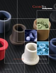
t h i c k - f i l m ceramic substrates design guide - CoorsTek
t h i c k - f i l m ceramic substrates design guide - CoorsTek
t h i c k - f i l m ceramic substrates design guide - CoorsTek

You also want an ePaper? Increase the reach of your titles
YUMPU automatically turns print PDFs into web optimized ePapers that Google loves.
As-Fired Substrates Design Guidelines<br />
The following <strong>design</strong> standards represent factors that should be considered to ensure optimal substrate<br />
<strong>design</strong> and material selection. Material samples are available on request so that the <strong>design</strong> or process<br />
engineer can determine, by proof test, the product specifications that best fit the process needs.<br />
Materials<br />
AD-96R<br />
Thick Film<br />
ADS-96R Thick-Film <strong>substrates</strong> are engineered<br />
to minimize as-fired resistor variations<br />
and maximize aged adhesion values.<br />
Superior resistor stability is achieved by<br />
controlling the <strong>substrates</strong>’ effects on the<br />
temperature coefficient of resistance. ADS-<br />
96R is particularly well suited for small<br />
geometry, high resistor value circuitry.<br />
ADOS-90R<br />
Opaque<br />
ADOS-90R (opaque) is the alumina substrate<br />
material of choice for light-sensitive<br />
semiconductor device applications.<br />
ASDR-96R<br />
Thick Film DuraStrate<br />
ADSR-96R Thick-Film DuraStrate <strong>substrates</strong><br />
are a fine-grained material which offers<br />
greater than a 20% increase in strength<br />
over the standard ADS-96R. DuraStrate<br />
material is primarily used in applications<br />
requiring <strong>substrates</strong> 0.020" thick or less.<br />
ADS-995R<br />
Mid-Film<br />
ADS-995R Mid-Film <strong>substrates</strong> are compatible<br />
with etchable ink and photo-formed<br />
systems, Mid-Film <strong>substrates</strong> have higher<br />
fl exural strength, higher thermal conductivity,<br />
higher dielectric constant with lower<br />
loss, uniform density and grain size.<br />
For expert<br />
assistance with<br />
As-Fired Dimensional Criteria<br />
your next project,<br />
Thickness Tolerances<br />
Length/Width Tolerances<br />
Camber Tolerances<br />
please call:<br />
Applies to thicknesses<br />
from 0.010" (0.254 mm)<br />
to 0.140" (3.556 mm)<br />
Economy<br />
± 1½ % NLT ± 0.010"<br />
(±0.254 mm)<br />
Standard<br />
≤ 0.003 in./in.<br />
(≤ 0.003 mm/mm)<br />
+1.800.799.1457<br />
in North America<br />
Standard<br />
± 10% NLT ± 0.002"<br />
(± 0.0508 mm)<br />
Standard<br />
± 1% NLT ± 0.004"<br />
(± 0.102 mm)<br />
Premium<br />
≤ 0.002 in./in.<br />
(≤ 0.002 mm/mm)<br />
Lapping services are<br />
available for tighter<br />
tolerances.<br />
Premium<br />
± 0.5% NLT ± 0.003"<br />
(± 0.076 mm)<br />
Tighter tolerances available<br />
upon request. Lapping<br />
services are also available.<br />
Hole Diameter<br />
Tolerance<br />
Hole-to-Hole Tolerance<br />
0.015"-0.029" (0.381mm -0.737mm)<br />
0.030"-0.099" (0.762mm-2.515mm)<br />
± 0.002" (± 0.051 mm)<br />
± 0.003" (± 0.076 mm)<br />
Standard<br />
± 1% NLT ± 0.004"<br />
(± 0.102 mm)<br />
≥0.100" (2.540mm)<br />
± 0.005" (± 0.127 mm)<br />
or ± 1%, whichever<br />
is greater<br />
Premium<br />
± 0.5% NLT ± 0.003"<br />
(± 0.076 mm)<br />
Thick Film