t h i c k - f i l m ceramic substrates design guide - CoorsTek
t h i c k - f i l m ceramic substrates design guide - CoorsTek
t h i c k - f i l m ceramic substrates design guide - CoorsTek

Create successful ePaper yourself
Turn your PDF publications into a flip-book with our unique Google optimized e-Paper software.
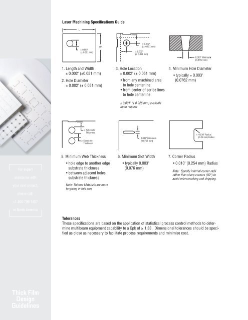
Laser Machining Specifi cations Guide<br />
1. Length and Width<br />
± 0.002" (±0.051 mm)<br />
2. Hole Diameter<br />
± 0.002" (± 0.051 mm)<br />
3. Hole Location<br />
± 0.002" (± 0.051 mm)<br />
• from any machined area<br />
to hole centerline<br />
• from center of scribe lines<br />
to hole centerline<br />
4. Minimum Hole Diameter<br />
• typically = 0.003"<br />
(0.0762 mm)<br />
± 0.001" (± 0.026 mm) available<br />
upon request<br />
5. Minimum Web Thickness<br />
6. Minimum Slot Width<br />
7. Corner Radius<br />
For expert<br />
assistance with<br />
• hole edge to another edge<br />
substrate thickness<br />
• between adjacent holes<br />
substrate thickness<br />
• typically 0.003"<br />
(0.076 mm)<br />
• 0.010" (0.254 mm) Radius<br />
Note: Specify internal corner radii<br />
rather than sharp corners (90°) to<br />
avoid microcracking and chipping.<br />
your next project,<br />
please call:<br />
Note: Thinner Materials are more<br />
forgiving in this area<br />
+1.800.799.1457<br />
in North America<br />
Tolerances<br />
These specifications are based on the application of statistical process control methods to determine<br />
multibeam equipment capability to a Cpk of ≥ 1.33. Dimensional tolerances should be specifi<br />
ed as close as necessary to facilitate process requirements and minimize cost.<br />
Thick Film