TSOP17.. Photo Modules for PCM Remote Control Systems - Micropik
TSOP17.. Photo Modules for PCM Remote Control Systems - Micropik
TSOP17.. Photo Modules for PCM Remote Control Systems - Micropik

You also want an ePaper? Increase the reach of your titles
YUMPU automatically turns print PDFs into web optimized ePapers that Google loves.
<strong>TSOP17.</strong>.<br />
Vishay Telefunken<br />
<strong>Photo</strong> <strong>Modules</strong> <strong>for</strong> <strong>PCM</strong> <strong>Remote</strong> <strong>Control</strong> <strong>Systems</strong><br />
Available types <strong>for</strong> different carrier frequencies<br />
Type fo Type fo<br />
TSOP1730 30 kHz TSOP1733 33 kHz<br />
TSOP1736 36 kHz TSOP1737 36.7 kHz<br />
TSOP1738 38 kHz TSOP1740 40 kHz<br />
TSOP1756<br />
56 kHz<br />
Description<br />
The <strong>TSOP17.</strong>. – series are miniaturized receivers <strong>for</strong><br />
infrared remote control systems. PIN diode and<br />
preamplifier are assembled on lead frame, the epoxy<br />
package is designed as IR filter.<br />
The demodulated output signal can directly be<br />
decoded by a microprocessor. <strong>TSOP17.</strong>. is the<br />
standard IR remote control receiver series,<br />
supporting all major transmission codes.<br />
GND<br />
V S<br />
OUT<br />
94 8691<br />
Features<br />
<br />
<br />
<br />
<br />
<strong>Photo</strong> detector and preamplifier in one package<br />
Internal filter <strong>for</strong> <strong>PCM</strong> frequency<br />
Improved shielding against electrical<br />
field disturbance<br />
TTL and CMOS compatibility<br />
<br />
<br />
<br />
<br />
<br />
Output active low<br />
Low power consumption<br />
High immunity against ambient light<br />
Continuous data transmission possible<br />
(1200 bit/s)<br />
Suitable burst length ≥10 cycles/burst<br />
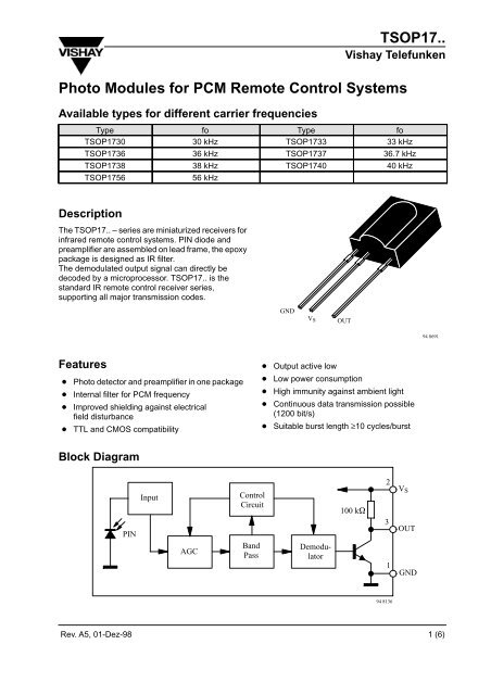
Block Diagram<br />
PIN<br />
Input<br />
<strong>Control</strong><br />
Circuit<br />
100 k<br />
2<br />
3<br />
V S<br />
OUT<br />
AGC<br />
Band<br />
Pass<br />
Demodulator<br />
1<br />
GND<br />
94 8136<br />
Rev. A5, 01-Dez-98 1 (6)
<strong>TSOP17.</strong>.<br />
Vishay Telefunken<br />
Absolute Maximum Ratings<br />
T amb = 25 C<br />
Parameter Test Conditions Symbol Value Unit<br />
Supply Voltage (Pin 2) V S –0.3...6.0 V<br />
Supply Current (Pin 2) I S 5 mA<br />
Output Voltage (Pin 3) V O –0.3...6.0 V<br />
Output Current (Pin 3) I O 5 mA<br />
Junction Temperature T j 100 C<br />
Storage Temperature Range T stg –25...+85 C<br />
Operating Temperature Range T amb –25...+85 C<br />
Power Consumption (T amb 85 C) P tot 50 mW<br />
Soldering Temperature t 10 s, 1 mm from case T sd 260 C<br />
Basic Characteristics<br />
T amb = 25 C<br />
Parameter Test Conditions Symbol Min Typ Max Unit<br />
Supply Current (Pin 2) V S = 5 V, E v = 0 I SD 0.4 0.6 0.8 mA<br />
V S = 5 V, E v = 40 klx, sunlight I SH 1.0 mA<br />
Transmission Distance E v = 0, test signal see fig.7,<br />
d 35 m<br />
IR diode TSIP5201, I F = 400 mA<br />
Output Voltage Low (Pin 3) I OSL = 0.5 mA,<br />
V OSL 250 mV<br />
E e = 0.7 mW/m 2 , f = f o , t p /T = 0.4<br />
Irradiance (30 – 40 kHz) Pulse width tolerance:<br />
E e min 0.35 0.5 mW/m 2<br />
t pi – 5/f o < t po < t pi + 6/f o ,<br />
test signal (see fig.7)<br />
Irradiance (56 kHz) Pulse width tolerance:<br />
E e min 0.4 0.6 mW/m 2<br />
t pi – 5/f o < t po < t pi + 6/f o ,<br />
test signal (see fig.7)<br />
Irradiance E e max 30 W/m 2<br />
Directivity Angle of half transmission distance ϕ 1/2 ±45 deg<br />
Application Circuit<br />
330 *) +5V **)<br />
TSAL62..<br />
<strong>TSOP17.</strong>.<br />
2<br />
3<br />
4.7 F *)<br />
>10 k<br />
optional<br />
C<br />
96 12108<br />
1<br />
GND<br />
*) only necessary to suppress power supply disturbances<br />
**) tolerated supply voltage range : 4.5V
<strong>TSOP17.</strong>.<br />
Vishay Telefunken<br />
Typical Characteristics (T amb = 25 C unless otherwise specified)<br />
e E min / e E – Rel. Responsitivity<br />
94 8143<br />
1.0<br />
0.8<br />
0.6<br />
0.4<br />
0.2<br />
f = f 0 5%<br />
f ( 3 dB ) = f 0 /10<br />
0.0<br />
0.7 0.8 0.9 1.0 1.1<br />
f/f 0 – Relative Frequency<br />
1.2<br />
1.3<br />
E e min – Threshold Irradiance ( mW/m )<br />
2<br />
94 8147<br />
2.0<br />
1.6<br />
1.2<br />
0.8<br />
0.4<br />
f(E)=f 0<br />
0.0<br />
0.0 0.4 0.8 1.2 1.6<br />
E – Field Strength of Disturbance ( kV / m )<br />
2.0<br />
Figure 1. Frequency Dependence of Responsivity<br />
Figure 4. Sensitivity vs. Electric Field Disturbances<br />
t po – Output Pulse Length (ms)<br />
96 12110<br />
1.0<br />
0.9<br />
0.8<br />
0.7<br />
0.6<br />
0.5<br />
0.4<br />
0.3<br />
0.2<br />
0.1<br />
Input burst duration<br />
= 950 nm,<br />
optical test signal, fig.7<br />
0<br />
0.1 1.0 10.0 100.0 1000.0 10000.0<br />
E e – Irradiance ( mW/m 2 )<br />
Figure 2. Sensitivity in Dark Ambient<br />
E e min – Threshold Irradiance ( mW/m )<br />
2<br />
10<br />
1<br />
f = f 0<br />
10 kHz<br />
100 Hz<br />
0.1<br />
0.01 0.1 1 10 100<br />
1 kHz<br />
1000<br />
94 9106 V sRMS – AC Voltage on DC Supply Voltage ( mV )<br />
Figure 5. Sensitivity vs. Supply Voltage Disturbances<br />
E e min – Threshold Irradiance (mW/m 2 )<br />
96 12111<br />
5.0<br />
4.5<br />
Correlation with ambient light sources<br />
( Disturbance effect ) : 10W/m 2 1.4 klx<br />
4.0 ( Stand.illum.A, T = 2855 K ) 8.2 klx<br />
3.5 ( Daylight, T = 5900 K )<br />
3.0<br />
2.5<br />
2.0<br />
1.5<br />
Ambient, = 950 nm<br />
1.0<br />
0.5<br />
0<br />
0.01 0.10 1.00 10.00 100.00<br />
E – DC Irradiance (W/m 2 )<br />
Figure 3. Sensitivity in Bright Ambient<br />
E e min – Threshold Irradiance (mW/m 2 )<br />
96 12112<br />
1.0<br />
0.9<br />
0.8<br />
0.7<br />
0.6<br />
0.5<br />
0.4<br />
0.3<br />
0.2<br />
0.1<br />
Sensitivity in dark ambient<br />
0<br />
–30 –15 0 15 30 45 60 75 90<br />
T amb – Ambient Temperature ( °C )<br />
Figure 6. Sensitivity vs. Ambient Temperature<br />
Rev. A5, 01-Dez-98 3 (6)
<strong>TSOP17.</strong>.<br />
Vishay Telefunken<br />
E e<br />
V O<br />
V OH<br />
V OL<br />
E e<br />
V O<br />
V OH<br />
V OL<br />
Optical Test Signal<br />
( IR diode TSIP 5201, I F = 0.4 A, 30 pulses, f = f 0 , T = 10 ms<br />
Output Signal<br />
t pi *<br />
T<br />
* t pi 10/fo is recommended <strong>for</strong> optimal function<br />
1 ) 7/f 0 < t d < 15/f 0<br />
2 ) t po = t pi 6/f 0<br />
t d<br />
1 ) t po<br />
2 )<br />
Figure 7. Output Function<br />
Optical Test Signal<br />
600 s 600 s<br />
T = 60 ms<br />
Output Signal, ( see Fig.10 )<br />
t<br />
t<br />
96 12109<br />
T on T off<br />
t<br />
94 8134<br />
Figure 8. Output Function<br />
t<br />
T on ,T off – Output Pulse Length (ms)<br />
96 12114<br />
I – Supply Current ( mA )<br />
s<br />
96 12115<br />
1.0<br />
0.9<br />
0.8<br />
T on<br />
0.7<br />
0.6<br />
0.5<br />
0.4<br />
T off<br />
0.3<br />
0.2<br />
= 950 nm,<br />
optical test signal, fig.8<br />
0.1<br />
0<br />
0.1 1.0 10.0 100.0 1000.0 10000.0<br />
E e – Irradiance (mW/m 2 )<br />
Figure 10. Output Pulse Diagram<br />
1.0<br />
0.9<br />
0.8<br />
V s = 5 V<br />
0.7<br />
0.6<br />
0.5<br />
0.4<br />
0.3<br />
0.2<br />
0.1<br />
0<br />
–30 –15 0 15 30 45 60 75 90<br />
T amb – Ambient Temperature ( °C )<br />
Figure 11. Supply Current vs. Ambient Temperature<br />
E e min – Threshold Irradiance (mW/m 2 )<br />
96 12113<br />
3.0<br />
2.5<br />
2.0<br />
1.5<br />
1.0<br />
0.5<br />
N=16<br />
pulses per burst<br />
0<br />
0 0.1 0.2 0.3 0.4 0.5 0.6 0.7<br />
t p /T – Duty Cycle<br />
N=32<br />
S ( ) rel – Relative Spectral Sensitivity<br />
94 8408<br />
1.2<br />
1.0<br />
0.8<br />
0.6<br />
0.4<br />
0.2<br />
0<br />
750 850 950 1050<br />
– Wavelength ( nm )<br />
1150<br />
Figure 9. Sensitivity vs. Duty Cycle<br />
Figure 12. Relative Spectral Sensitivity vs. Wavelength<br />
4 (6)<br />
Rev. A5, 01-Dez-98
<strong>TSOP17.</strong>.<br />
Vishay Telefunken<br />
0°<br />
10° 20°<br />
30°<br />
0°<br />
10° 20°<br />
30°<br />
1.0<br />
40°<br />
1.0<br />
40°<br />
0.9<br />
50°<br />
0.9<br />
50°<br />
0.8<br />
60°<br />
0.8<br />
60°<br />
0.7<br />
70°<br />
80°<br />
0.7<br />
70°<br />
80°<br />
0.6<br />
0.4 0.2 0 0.2 0.4 0.6<br />
0.6<br />
0.4 0.2 0 0.2 0.4 0.6<br />
95 11339p2<br />
d rel – Relative Transmission Distance<br />
95 11340p2<br />
d rel – Relative Transmission Distance<br />
Figure 13. Vertical Directivity ϕ y<br />
Figure 14. Horizontal Directivity ϕ x<br />
Dimensions in mm<br />
96 12116<br />
Rev. A5, 01-Dez-98 5 (6)
<strong>TSOP17.</strong>.<br />
Vishay Telefunken<br />
Ozone Depleting Substances Policy Statement<br />
It is the policy of Vishay Semiconductor GmbH to<br />
1. Meet all present and future national and international statutory requirements.<br />
2. Regularly and continuously improve the per<strong>for</strong>mance of our products, processes, distribution and operating<br />
systems with respect to their impact on the health and safety of our employees and the public, as well as their<br />
impact on the environment.<br />
It is particular concern to control or eliminate releases of those substances into the atmosphere which are known<br />
as ozone depleting substances (ODSs).<br />
The Montreal Protocol (1987) and its London Amendments (1990) intend to severely restrict the use of ODSs and<br />
<strong>for</strong>bid their use within the next ten years. Various national and international initiatives are pressing <strong>for</strong> an earlier ban<br />
on these substances.<br />
Vishay Semiconductor GmbH has been able to use its policy of continuous improvements to eliminate the use<br />
of ODSs listed in the following documents.<br />
1. Annex A, B and list of transitional substances of the Montreal Protocol and the London Amendments respectively<br />
2. Class I and II ozone depleting substances in the Clean Air Act Amendments of 1990 by the Environmental<br />
Protection Agency (EPA) in the USA<br />
3. Council Decision 88/540/EEC and 91/690/EEC Annex A, B and C (transitional substances) respectively.<br />
Vishay Semiconductor GmbH can certify that our semiconductors are not manufactured with ozone depleting<br />
substances and do not contain such substances.<br />
We reserve the right to make changes to improve technical design and may do so without further notice.<br />
Parameters can vary in different applications. All operating parameters must be validated <strong>for</strong> each customer<br />
application by the customer. Should the buyer use Vishay-Telefunken products <strong>for</strong> any unintended or unauthorized<br />
application, the buyer shall indemnify Vishay-Telefunken against all claims, costs, damages, and expenses, arising out<br />
of, directly or indirectly, any claim of personal damage, injury or death associated with such unintended or<br />
unauthorized use.<br />
Vishay Semiconductor GmbH, P.O.B. 3535, D-74025 Heilbronn, Germany<br />
Telephone: 49 (0)7131 67 2831, Fax number: 49 (0)7131 67 2423<br />
6 (6)<br />
Rev. A5, 01-Dez-98