Advanced Solid State Physics
Advanced Solid State Physics
Advanced Solid State Physics

Create successful ePaper yourself
Turn your PDF publications into a flip-book with our unique Google optimized e-Paper software.
<strong>Advanced</strong> <strong>Solid</strong> <strong>State</strong> <strong>Physics</strong><br />
Version 2009:<br />
Michael Mayrhofer-R., Patrick Kraus, Christoph Heil, Hannes Brandner,<br />
Nicola Schlatter, Immanuel Mayrhuber, Stefan Kirnstötter,<br />
Alexander Volk, Gernot Kapper, Reinhold Hetzel<br />
Version 2010: Martin Nuss<br />
Version 2011: Christopher Albert, Max Sorantin, Benjamin Stickler<br />
TU Graz, SS 2011<br />
Lecturer: Univ. Prof. Ph.D. Peter Hadley
TU Graz, SS 2010<br />
<strong>Advanced</strong> <strong>Solid</strong> <strong>State</strong> <strong>Physics</strong><br />
Contents<br />
1 What is <strong>Solid</strong> <strong>State</strong> <strong>Physics</strong> 1<br />
2 Schrödinger Equation 2<br />
3 Quantization 3<br />
3.1 Quantization . . . . . . . . . . . . . . . . . . . . . . . . . . . . . . . . . . . . . . . . . 5<br />
3.1.1 Quantization of the Harmonic Oscillator . . . . . . . . . . . . . . . . . . . . . . 6<br />
3.1.2 Quantization of the Magnetic Flux . . . . . . . . . . . . . . . . . . . . . . . . . 7<br />
3.1.3 Quantisation of a charged particle in a magnetic field (with spin) . . . . . . . . 8<br />
3.1.4 Dissipation . . . . . . . . . . . . . . . . . . . . . . . . . . . . . . . . . . . . . . 11<br />
4 Quantization of the Electromagnetic Field - Quantization Recipe 12<br />
4.1 Thermodynamic Quantities . . . . . . . . . . . . . . . . . . . . . . . . . . . . . . . . . 17<br />
4.1.1 Recipe for the Quantization of Fields . . . . . . . . . . . . . . . . . . . . . . . . 18<br />
5 Photonic Crystals 19<br />
5.1 Intruduction: Plane Waves in Crystals . . . . . . . . . . . . . . . . . . . . . . . . . . . 19<br />
5.2 Empty Lattice Approximation (Photons) . . . . . . . . . . . . . . . . . . . . . . . . . . 22<br />
5.3 Central Equations . . . . . . . . . . . . . . . . . . . . . . . . . . . . . . . . . . . . . . 23<br />
5.4 Estimate the Size of the Photonic Bandgap . . . . . . . . . . . . . . . . . . . . . . . . 24<br />
5.5 Density of <strong>State</strong>s . . . . . . . . . . . . . . . . . . . . . . . . . . . . . . . . . . . . . . . 25<br />
5.6 Photon Density of <strong>State</strong>s . . . . . . . . . . . . . . . . . . . . . . . . . . . . . . . . . . 26<br />
6 Phonons 27<br />
6.1 Linear Chain . . . . . . . . . . . . . . . . . . . . . . . . . . . . . . . . . . . . . . . . . 27<br />
6.2 Simple Cubic . . . . . . . . . . . . . . . . . . . . . . . . . . . . . . . . . . . . . . . . . 30<br />
6.2.1 Raman Spectroscopy . . . . . . . . . . . . . . . . . . . . . . . . . . . . . . . . . 32<br />
7 Electrons 34<br />
7.1 Free Electron Fermi Gas . . . . . . . . . . . . . . . . . . . . . . . . . . . . . . . . . . . 34<br />
7.1.1 Fermi Energy . . . . . . . . . . . . . . . . . . . . . . . . . . . . . . . . . . . . . 34<br />
7.1.2 Chemical Potential . . . . . . . . . . . . . . . . . . . . . . . . . . . . . . . . . . 35<br />
7.1.3 Sommerfeld Expansion . . . . . . . . . . . . . . . . . . . . . . . . . . . . . . . . 36<br />
7.1.4 ARPES . . . . . . . . . . . . . . . . . . . . . . . . . . . . . . . . . . . . . . . . 39<br />
7.2 Electronic Band Structure Calculations . . . . . . . . . . . . . . . . . . . . . . . . . . 40<br />
7.2.1 Empty Lattice Approximation . . . . . . . . . . . . . . . . . . . . . . . . . . . 41<br />
7.2.2 Plane Wave Method - Central Equations . . . . . . . . . . . . . . . . . . . . . . 43<br />
7.2.3 Tight Binding Model . . . . . . . . . . . . . . . . . . . . . . . . . . . . . . . . . 47<br />
7.2.4 Graphene . . . . . . . . . . . . . . . . . . . . . . . . . . . . . . . . . . . . . . . 55<br />
7.2.5 Carbon nanotubes . . . . . . . . . . . . . . . . . . . . . . . . . . . . . . . . . . 57<br />
7.3 Bandstructure of Metals and Semiconductors . . . . . . . . . . . . . . . . . . . . . . . 61<br />
7.4 Direct and Indirect Bandgaps . . . . . . . . . . . . . . . . . . . . . . . . . . . . . . . . 67<br />
8 Crystal <strong>Physics</strong> 69<br />
8.1 Stress and Strain . . . . . . . . . . . . . . . . . . . . . . . . . . . . . . . . . . . . . . . 69<br />
i
TU Graz, SS 2010<br />
<strong>Advanced</strong> <strong>Solid</strong> <strong>State</strong> <strong>Physics</strong><br />
8.2 Statistical <strong>Physics</strong> . . . . . . . . . . . . . . . . . . . . . . . . . . . . . . . . . . . . . . 70<br />
8.3 Crystal Symmetries . . . . . . . . . . . . . . . . . . . . . . . . . . . . . . . . . . . . . . 72<br />
8.4 Example - Birefringence . . . . . . . . . . . . . . . . . . . . . . . . . . . . . . . . . . . 75<br />
9 Magnetism and Response to Electric and Magnetic Fields 76<br />
9.1 Introduction: Electric and Magnetic Fields . . . . . . . . . . . . . . . . . . . . . . . . 76<br />
9.2 Magnetic Fields . . . . . . . . . . . . . . . . . . . . . . . . . . . . . . . . . . . . . . . . 76<br />
9.3 Magnetic Response of Atoms and Molecules . . . . . . . . . . . . . . . . . . . . . . . . 78<br />
9.3.1 Diamagnetic Response . . . . . . . . . . . . . . . . . . . . . . . . . . . . . . . . 79<br />
9.3.2 Paramagnetic Response . . . . . . . . . . . . . . . . . . . . . . . . . . . . . . . 81<br />
9.4 Free Particles in a Weak Magnetic Field . . . . . . . . . . . . . . . . . . . . . . . . . . 81<br />
9.5 Ferromagnetism . . . . . . . . . . . . . . . . . . . . . . . . . . . . . . . . . . . . . . . . 86<br />
10 Transport Regimes 92<br />
10.1 Linear Response Theory . . . . . . . . . . . . . . . . . . . . . . . . . . . . . . . . . . . 92<br />
10.2 Ballistic Transport . . . . . . . . . . . . . . . . . . . . . . . . . . . . . . . . . . . . . . 94<br />
10.3 Drift-Diffusion . . . . . . . . . . . . . . . . . . . . . . . . . . . . . . . . . . . . . . . . 95<br />
10.4 Diffusive and Ballistic Transport . . . . . . . . . . . . . . . . . . . . . . . . . . . . . . 96<br />
10.5 Skin depth . . . . . . . . . . . . . . . . . . . . . . . . . . . . . . . . . . . . . . . . . . . 99<br />
11 Quasiparticles 102<br />
11.1 Fermi Liquid Theory . . . . . . . . . . . . . . . . . . . . . . . . . . . . . . . . . . . . . 102<br />
11.2 Particle like Quasiparticles . . . . . . . . . . . . . . . . . . . . . . . . . . . . . . . . . . 103<br />
11.2.1 Electrons and Holes . . . . . . . . . . . . . . . . . . . . . . . . . . . . . . . . . 103<br />
11.2.2 Bogoliubov Quasiparticles . . . . . . . . . . . . . . . . . . . . . . . . . . . . . . 103<br />
11.2.3 Polarons . . . . . . . . . . . . . . . . . . . . . . . . . . . . . . . . . . . . . . . . 103<br />
11.2.4 Bipolarons . . . . . . . . . . . . . . . . . . . . . . . . . . . . . . . . . . . . . . 103<br />
11.2.5 Mott Wannier Excitons . . . . . . . . . . . . . . . . . . . . . . . . . . . . . . . 103<br />
11.3 Collective modes . . . . . . . . . . . . . . . . . . . . . . . . . . . . . . . . . . . . . . . 103<br />
11.3.1 Phonons . . . . . . . . . . . . . . . . . . . . . . . . . . . . . . . . . . . . . . . . 103<br />
11.3.2 Polaritons . . . . . . . . . . . . . . . . . . . . . . . . . . . . . . . . . . . . . . . 104<br />
11.3.3 Magnons . . . . . . . . . . . . . . . . . . . . . . . . . . . . . . . . . . . . . . . 106<br />
11.3.4 Plasmons . . . . . . . . . . . . . . . . . . . . . . . . . . . . . . . . . . . . . . . 110<br />
11.3.5 Surface Plasmons . . . . . . . . . . . . . . . . . . . . . . . . . . . . . . . . . . . 112<br />
11.3.6 Frenkel Excitations . . . . . . . . . . . . . . . . . . . . . . . . . . . . . . . . . . 113<br />
11.4 Translational Symmetry . . . . . . . . . . . . . . . . . . . . . . . . . . . . . . . . . . . 113<br />
11.5 Occupation . . . . . . . . . . . . . . . . . . . . . . . . . . . . . . . . . . . . . . . . . . 114<br />
11.6 Experimental techniques . . . . . . . . . . . . . . . . . . . . . . . . . . . . . . . . . . . 115<br />
11.6.1 Raman Spectroscopy . . . . . . . . . . . . . . . . . . . . . . . . . . . . . . . . . 115<br />
11.6.2 EELS . . . . . . . . . . . . . . . . . . . . . . . . . . . . . . . . . . . . . . . . . 115<br />
11.6.3 Inelastic Scattering . . . . . . . . . . . . . . . . . . . . . . . . . . . . . . . . . . 115<br />
11.6.4 Photoemission . . . . . . . . . . . . . . . . . . . . . . . . . . . . . . . . . . . . 115<br />
12 Electron-electron interactions, Quantum electronics 116<br />
12.1 Electron Screening . . . . . . . . . . . . . . . . . . . . . . . . . . . . . . . . . . . . . . 116<br />
ii
TU Graz, SS 2010<br />
<strong>Advanced</strong> <strong>Solid</strong> <strong>State</strong> <strong>Physics</strong><br />
12.2 Single electron effects . . . . . . . . . . . . . . . . . . . . . . . . . . . . . . . . . . . . 118<br />
12.2.1 Tunnel Junctions . . . . . . . . . . . . . . . . . . . . . . . . . . . . . . . . . . . 118<br />
12.2.2 Single Electron Transistor . . . . . . . . . . . . . . . . . . . . . . . . . . . . . . 120<br />
12.3 Electronic phase transitions . . . . . . . . . . . . . . . . . . . . . . . . . . . . . . . . . 125<br />
12.3.1 Mott Transition . . . . . . . . . . . . . . . . . . . . . . . . . . . . . . . . . . . 125<br />
12.3.2 Peierls Transition . . . . . . . . . . . . . . . . . . . . . . . . . . . . . . . . . . . 126<br />
13 Optical Processes 131<br />
13.1 Optical Properties of Materials . . . . . . . . . . . . . . . . . . . . . . . . . . . . . . . 132<br />
13.1.1 Dielectric Response of Insulators . . . . . . . . . . . . . . . . . . . . . . . . . . 133<br />
13.1.2 Inter- and Intraband Transition . . . . . . . . . . . . . . . . . . . . . . . . . . . 136<br />
13.2 Collisionless Metal . . . . . . . . . . . . . . . . . . . . . . . . . . . . . . . . . . . . . . 137<br />
13.3 Diffusive Metals . . . . . . . . . . . . . . . . . . . . . . . . . . . . . . . . . . . . . . . . 139<br />
13.3.1 Dielectric Function . . . . . . . . . . . . . . . . . . . . . . . . . . . . . . . . . . 140<br />
14 Dielectrics and Ferroelectrics 143<br />
14.1 Excitons . . . . . . . . . . . . . . . . . . . . . . . . . . . . . . . . . . . . . . . . . . . . 143<br />
14.1.1 Introduction . . . . . . . . . . . . . . . . . . . . . . . . . . . . . . . . . . . . . 143<br />
14.1.2 Mott Wannier Excitons . . . . . . . . . . . . . . . . . . . . . . . . . . . . . . . 143<br />
14.1.3 Frenkel excitons . . . . . . . . . . . . . . . . . . . . . . . . . . . . . . . . . . . 144<br />
14.2 Optical measurements . . . . . . . . . . . . . . . . . . . . . . . . . . . . . . . . . . . . 146<br />
14.2.1 Introduction . . . . . . . . . . . . . . . . . . . . . . . . . . . . . . . . . . . . . 146<br />
14.2.2 Ellipsometry . . . . . . . . . . . . . . . . . . . . . . . . . . . . . . . . . . . . . 146<br />
14.2.3 Reflection electron energy loss spectroscopy . . . . . . . . . . . . . . . . . . . . 147<br />
14.2.4 Photo emission spectroscopy . . . . . . . . . . . . . . . . . . . . . . . . . . . . 147<br />
14.2.5 Raman spectroscopy . . . . . . . . . . . . . . . . . . . . . . . . . . . . . . . . . 148<br />
14.3 Dielectrics . . . . . . . . . . . . . . . . . . . . . . . . . . . . . . . . . . . . . . . . . . . 152<br />
14.3.1 Introduction . . . . . . . . . . . . . . . . . . . . . . . . . . . . . . . . . . . . . 152<br />
14.3.2 Polarizability . . . . . . . . . . . . . . . . . . . . . . . . . . . . . . . . . . . . . 154<br />
14.4 Structural phase transitions . . . . . . . . . . . . . . . . . . . . . . . . . . . . . . . . . 156<br />
14.4.1 Introduction . . . . . . . . . . . . . . . . . . . . . . . . . . . . . . . . . . . . . 156<br />
14.4.2 Example: Tin . . . . . . . . . . . . . . . . . . . . . . . . . . . . . . . . . . . . . 157<br />
14.4.3 Example: Iron . . . . . . . . . . . . . . . . . . . . . . . . . . . . . . . . . . . . 159<br />
14.4.4 Ferroelectricity . . . . . . . . . . . . . . . . . . . . . . . . . . . . . . . . . . . . 159<br />
14.4.5 Pyroelectricity . . . . . . . . . . . . . . . . . . . . . . . . . . . . . . . . . . . . 162<br />
14.4.6 Antiferroelectricity . . . . . . . . . . . . . . . . . . . . . . . . . . . . . . . . . . 162<br />
14.4.7 Piezoelectricity . . . . . . . . . . . . . . . . . . . . . . . . . . . . . . . . . . . . 163<br />
14.4.8 Polarization . . . . . . . . . . . . . . . . . . . . . . . . . . . . . . . . . . . . . . 164<br />
14.5 Landau Theory of Phase Transitions . . . . . . . . . . . . . . . . . . . . . . . . . . . . 165<br />
14.5.1 Second Order Phase Transitions . . . . . . . . . . . . . . . . . . . . . . . . . . 165<br />
14.5.2 First Order Phase Transitions . . . . . . . . . . . . . . . . . . . . . . . . . . . . 169<br />
15 Summary: Silicon 171<br />
16 Superconductivity 177<br />
16.1 Introduction . . . . . . . . . . . . . . . . . . . . . . . . . . . . . . . . . . . . . . . . . . 177<br />
iii
TU Graz, SS 2010<br />
<strong>Advanced</strong> <strong>Solid</strong> <strong>State</strong> <strong>Physics</strong><br />
16.2 Experimental Observations . . . . . . . . . . . . . . . . . . . . . . . . . . . . . . . . . 180<br />
16.2.1 Fundamentals . . . . . . . . . . . . . . . . . . . . . . . . . . . . . . . . . . . . . 180<br />
16.2.2 Meissner - Ochsenfeld Effect . . . . . . . . . . . . . . . . . . . . . . . . . . 181<br />
16.2.3 Heat Capacity . . . . . . . . . . . . . . . . . . . . . . . . . . . . . . . . . . . . 182<br />
16.2.4 Isotope Effect . . . . . . . . . . . . . . . . . . . . . . . . . . . . . . . . . . . . . 183<br />
16.3 Phenomenological Description . . . . . . . . . . . . . . . . . . . . . . . . . . . . . . . . 185<br />
16.3.1 Thermodynamic Considerations . . . . . . . . . . . . . . . . . . . . . . . . . . . 185<br />
16.3.2 The London Equations . . . . . . . . . . . . . . . . . . . . . . . . . . . . . . . 186<br />
16.3.3 Ginzburg - Landau Equations . . . . . . . . . . . . . . . . . . . . . . . . . . 187<br />
16.4 Microscopic Theories . . . . . . . . . . . . . . . . . . . . . . . . . . . . . . . . . . . . . 191<br />
16.4.1 BCS Theory of Superconductivity . . . . . . . . . . . . . . . . . . . . . . . . . 191<br />
16.4.2 Some BCS Results . . . . . . . . . . . . . . . . . . . . . . . . . . . . . . . . . . 191<br />
16.4.3 Cooper Pairs . . . . . . . . . . . . . . . . . . . . . . . . . . . . . . . . . . . . 193<br />
16.4.4 Flux Quantization . . . . . . . . . . . . . . . . . . . . . . . . . . . . . . . . . . 194<br />
16.4.5 Single Particle Tunneling . . . . . . . . . . . . . . . . . . . . . . . . . . . . . . 197<br />
16.4.6 The Josephson Effect . . . . . . . . . . . . . . . . . . . . . . . . . . . . . . . . 197<br />
16.4.7 SQUID . . . . . . . . . . . . . . . . . . . . . . . . . . . . . . . . . . . . . . . . 199<br />
iv
TU Graz, SS 2010<br />
<strong>Advanced</strong> <strong>Solid</strong> <strong>State</strong> <strong>Physics</strong><br />
1 What is <strong>Solid</strong> <strong>State</strong> <strong>Physics</strong><br />
<strong>Solid</strong> state physics is (still) the study of how atoms arrange themselves into solids and what properties<br />
these solids have.<br />
The atoms arrange in particular patterns because the patterns minimize the energy in a binding,<br />
which is typically with more than one neighbor in a solid. An ordered (periodic) arrangement is called<br />
crystal, a disordered arrangement is called amorphous.<br />
All the macroscopic properties like electrical conductivity, color, density, elasticity and more are determined<br />
by and can be calculated from the microscopic structure.<br />
1
TU Graz, SS 2010<br />
<strong>Advanced</strong> <strong>Solid</strong> <strong>State</strong> <strong>Physics</strong><br />
2 Schrödinger Equation<br />
The framework of most solid state physics theory is the Schrödinger equation of non relativistic<br />
quantum mechanics:<br />
i ∂Ψ<br />
∂t = −2<br />
2m ∇2 Ψ + V (r, t)Ψ (1)<br />
The most remarkable thing is the great variety of qualitativly different solutions to Schrödinger’s<br />
equation that can arise. In solid state physics you can calculate all properties with the Schrödinger<br />
equation, but the equation is intractable and can be only solved with approximations.<br />
For solving the equation numerically for a given system, the system and therewith Ψ are discretized<br />
into cubes of the relevant space. To solve it for an electron, about 10 6 elements are needed. This is<br />
not easy, but possible. But let’s have a look at an other example:<br />
For a gold atom with 79 electrons there are (in three dimensions) 3 · 79 terms for the kinetic energy in<br />
the Schrödinger equation. There are also 79 terms for the potential energy between the electrons and<br />
the nucleus. With the interaction of the electrons there are additionally 79·78<br />
2<br />
terms. So the solution for<br />
Ψ would be a complex function in 237(!) dimensions. For a numerically solution we have to discretize<br />
each of these 237 axis, let’s say in 100 divisions. This would give 100 237 = 10 474 hyper-cubes, where<br />
a solution is needed. That’s a lot, because there are just about 10 68 atoms in the Milky Way galaxy!<br />
Out of this it is possible to say:<br />
The Schrödinger equation explains everything but can explain nothing.<br />
Out of desperation: The model for a solid is simplified until the Schrödinger equation can be solved.<br />
Often this involves neglecting the electron-electron interactions. Back to the example of the gold atom<br />
this means that the resulting wavefunction is considered as a product of hydrogen wavefunctions.<br />
Because of this it is possible to solve the new equation exactly. The total wavefunction for the<br />
electrons must obey the Pauli exclusion principle. The sign of the wavefunction must change when<br />
two electrons are exchanged. The antisymmetric N electron wavefunctioncan can be written as a<br />
Slater determinant:<br />
∣ ∣∣∣∣∣∣∣∣∣ Ψ 1 (r 1 ) Ψ 1 (r 2 ) . . . Ψ 1 (r N )<br />
Ψ(r 1 , r 2 , ..., r N ) = √ 1<br />
Ψ 2 (r 1 ) Ψ 2 (r 2 ) . . . Ψ 2 (r N )<br />
. N! . . .. (2)<br />
.<br />
Ψ N (r 1 ) Ψ N (r 2 ) . . . Ψ N (r N ) ∣<br />
Exchanging two columns changes the sign of the determinant. If two columns are the same, the<br />
determinant is zero. There are still N!, in the example 79! (≈ 10 100 = 1 googol) terms.<br />
2
TU Graz, SS 2010<br />
<strong>Advanced</strong> <strong>Solid</strong> <strong>State</strong> <strong>Physics</strong><br />
3 Quantization<br />
The first topic in this chapter is the appearance of Rabi oscillations. For understanding their origin<br />
a few examples would be quite helpful.<br />
Ammonia molecule NH 3 :<br />
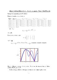
The first example is the ammonia molecule NH 3 , which is shown in fig. 1.<br />
Figure 1: left: Ammonia molecule; right: Nitrogen atom can change the side<br />
The nitrogen atom can either be on the "left" or on the "right" side of the plane, in which the hydrogen<br />
atoms are. The potential energy for this configuration is a double well potential, which is shown in<br />
fig. 2.<br />
2<br />
1.5<br />
1<br />
0.5<br />
energy / a.u.<br />
0<br />
−0.5<br />
−1<br />
−1.5<br />
−2<br />
−2.5<br />
−3<br />
−1.5 −1 −0.5 0 0.5 1 1.5<br />
x / a.u.<br />
Figure 2: Double-Well Potential of ammonia molecule<br />
The symmetric wavefunction for the ground state of the molecule has two maxima, where the potential<br />
has it’s minima. The antisymmetric wavefunction of the first excited state of the molecule has only one<br />
maximum in one of the minima of the potential, at the other potential minimum it has a minimum.<br />
If the molecule is prepared in a way that the nitrogen N is on just one side of the hydrogen plane,<br />
this is a superposition of the ground state and the first excited state of the molecule wavefunctions.<br />
It’s imagineable that the resulting wavefunction, which is not an eigenstate, has a maximum on the<br />
side where the nitrogen atom is prepared and nearly vanishes at the other side. But attention: The<br />
energies of the ground state and the first excited state are slightly different. Therefore the resulting<br />
3
TU Graz, SS 2010<br />
<strong>Advanced</strong> <strong>Solid</strong> <strong>State</strong> <strong>Physics</strong><br />
wavefunction doesn’t vanish completely on the other side! There is a small probability for the<br />
nitrogen atom to tunnel through the potential on the other side, which grows with time because the<br />
time developments of the symmetric (e iE 0 t<br />
<br />
) and antisymmetric (e iE 1 t<br />
) wavefunctions are different.<br />
This fact leads to the so called Rabi oscillations: In this example the probability that the nitrogen<br />
atom is on one side oscillates.<br />
Rabi oscillations appear like damped harmonic oscillations. The decay of the Rabi oscillations is<br />
called the decoherence time. The decay appears because the system is also interacting with it’s<br />
surrounding - other degrees of freedom.<br />
4
TU Graz, SS 2010<br />
<strong>Advanced</strong> <strong>Solid</strong> <strong>State</strong> <strong>Physics</strong><br />
3.1 Quantization<br />
For the quantization of a given system with well defined equations of motion it is necessary to<br />
guess a Lagrangian L(q i , ˙q i ), i.e. to construct a Lagrangian by inspection. q i are the positional<br />
coordinates and ˙q i the generalized velocities.<br />
With the Euler-Lagrange equations<br />
d ∂L<br />
− ∂L = 0 (3)<br />
dt ∂ ˙q i ∂q i<br />
it must be possible to come back to the equations of motion with the constructed Lagrangian. 1<br />
The next step is to get the conjugate variable p i :<br />
p i = ∂L<br />
∂ ˙q i<br />
(4)<br />
Then the Hamiltonian has to be derived with a Legendre transformation:<br />
H = ∑ i<br />
p i ˙q i − L (5)<br />
Now the conjugate variables have to be replaced by the given operators in quantum<br />
mechanics. For example the momentum p with<br />
p → −i∇.<br />
Now the Schrödinger equation<br />
HΨ(q) = EΨ(q) (6)<br />
is ready to be evaluated.<br />
1 There is no standard procedure for constructing a Lagrangian like in classical mechanics where the Lagrangian is<br />
constructed with the kinetic energy T and the potential U:<br />
L = T − U = 1 2 mẋ2 − U<br />
The mass m is the big problem - it isn’t always as well defined as for example in classical mechanics.<br />
5
TU Graz, SS 2010<br />
<strong>Advanced</strong> <strong>Solid</strong> <strong>State</strong> <strong>Physics</strong><br />
3.1.1 Quantization of the Harmonic Oscillator<br />
The first example how a given system can be quantized is a one dimensional harmonic oscillator. It’s<br />
assumed that just the equation of motion<br />
mẍ = −kx<br />
with m the mass and the spring constant k is known from this system. Now the Lagrangian L must<br />
be constructed by inspection:<br />
L(x, ẋ) = mẋ2<br />
2<br />
− kx2<br />
2<br />
It is the right one if the given equation of motion can be derived by the Euler-Lagrange eqn. (3), like<br />
in this example. The next step is to get the conjugate variable, the generalized momentum p:<br />
p = ∂L<br />
∂ẋ = mẋ<br />
Then the Hamiltonian has to be constructed with the Legendre transformation:<br />
H = ∑ i<br />
p i ˙q i − L = p2<br />
2m + kx2<br />
2 .<br />
With replacing the conjugate variable p with<br />
p → −i ∂<br />
∂x<br />
because of position space 2 and inserting in eqn. (6) the Schrödinger equation for the one dimensional<br />
harmonic oscillator is derived:<br />
− 2 ∂ 2 Ψ(x)<br />
2m ∂x 2<br />
+ kx2 Ψ(x) = EΨ(x)<br />
2<br />
2 position space: Ortsraum<br />
6
TU Graz, SS 2010<br />
<strong>Advanced</strong> <strong>Solid</strong> <strong>State</strong> <strong>Physics</strong><br />
Figure 3: Superconducting ring with a capacitor parallel to a Josephson junction<br />
3.1.2 Quantization of the Magnetic Flux<br />
The next example is the quantization of magnetic flux in a superconducting ring with a Josephson<br />
junction and a capacitor parallel to it (see fig. 3). The equivalent to the equations of motion is here<br />
the equation for current conservation:<br />
( )<br />
C ¨Φ 2πΦ<br />
+ I C sin = − Φ − Φ e<br />
Φ 0 L 1<br />
What are the terms of this equation? The charge Q in the capacitor with capacity C ist given by<br />
Q = C · V<br />
with V as the voltage applied. Derivate this equation after the time t gives the current I:<br />
˙Q = I = C · ˙V<br />
With Faraday’s law ˙Φ = V (Φ as the magnetic flux) this gives the first term for the current through<br />
the capacitor<br />
I = C · ¨Φ.<br />
The current I in a Josephson junction is given by<br />
( ) 2πΦ<br />
I = I c · sin<br />
Φ 0<br />
with the flux quantum Φ 0 , which is the second term. The third term comes from the relationship<br />
between the flux Φ in an inductor with inductivity L 1 and a current I:<br />
Φ = L 1 · I<br />
With the applied flux Φ e and the flux in the ring this results in<br />
I = Φ − Φ e<br />
L 1<br />
,<br />
which is the third term.<br />
In this example it isn’t as easy as before to construct a Lagrangian. But luckily we are quite smart<br />
and so the right Lagrangian is<br />
L(Φ, ˙Φ) = C ˙Φ 2<br />
2<br />
− (Φ − Φ e) 2<br />
2L 1<br />
( ) 2πΦ<br />
+ E j cos .<br />
Φ 0<br />
7
TU Graz, SS 2010<br />
<strong>Advanced</strong> <strong>Solid</strong> <strong>State</strong> <strong>Physics</strong><br />
The conjugate variable is<br />
∂L<br />
∂ ˙Φ = C ˙Φ = Q.<br />
Then the Hamiltonian via a Legendre transformation:<br />
H = Q ˙Φ − L = Q2<br />
2C + (Φ − Φ e) 2 ( ) 2πΦ<br />
− E j cos<br />
2L 1<br />
Φ 0<br />
Now the replacement of the conjugate variable, i.e. the quantization:<br />
Q → −i ∂<br />
∂Φ<br />
The result is the wanted Schrödinger equation for the given system:<br />
− 2 ∂ 2 Ψ(Φ)<br />
2C<br />
∂Φ 2 + (Φ − Φ e) 2<br />
2L 1<br />
( ) 2πΦ<br />
Ψ(Φ) − E j cos Ψ(Φ) = EΨ(Φ)<br />
Φ 0<br />
3.1.3 Quantisation of a charged particle in a magnetic field (with spin)<br />
For now we will neglect that the particle has spin, because in the quantisation we will treat the case<br />
of a constant magnetic field pointing in the z-direction. In this simplified case there is no contribution<br />
to the force from the spin interaction with the magnetic field (because it only adds a constant to the<br />
Hamiltonian which does not affect the equation of motion).<br />
We start with the equation of motion of a charged particle (without spin) in an EM-field, which is<br />
given by the Lorentz force law.<br />
F = m ∂2 r(t)<br />
∂t 2 = q(E + v × B) (7)<br />
One can check that a suitable Lagrangian is<br />
L(r, t) = mv2<br />
2<br />
− qφ + qv · A (8)<br />
where φ and A are the scalar and vector Potential, respectively. From the Lagrangian we get the<br />
generalized momentum (canonical conjugated variable)<br />
p i = ∂L<br />
∂ṙ x<br />
= mv x + qA x<br />
p = mv + qA (9)<br />
v(p) = 1 m (p − qA) 8
TU Graz, SS 2010<br />
<strong>Advanced</strong> <strong>Solid</strong> <strong>State</strong> <strong>Physics</strong><br />
The conjugated variable to position has now two components, the first therm in eqn.(9) mv which is<br />
the normal momentum. The second term qA which is called the field momentum. It enters in this<br />
equation because when a charged particle is accelerated it also creates a Magnetic field. The creation<br />
of the magnetic field takes some energy, which is then conserved in the field. When one then tries to<br />
stop the moving particle one has to overcome the kinetic energy plus the energy that is conserved in<br />
the magnetic field, because the magnetic field will keep pushing the charged particle in the direction<br />
it was going ( this is when you get back the energy that went into creating the field, also called self<br />
inductance).<br />
To construct the Hamiltonian we have to perform a Legendre transformation from the velocity v to<br />
the generalized momentum p.<br />
3∑<br />
H = p i v i (p i ) − L(r, v(p, t)<br />
i=1<br />
H = p · 1<br />
1<br />
(p − qA) −<br />
m 2m (p − qA)2 + qφ − q (p − qA) · A<br />
m<br />
Which then reduces to<br />
H = 1<br />
2m (p − qA)2 + qφ (10)<br />
Eqn.(10) is the Hamiltonian for a charged particle in an EM-field without Spin. The QM Hamiltonian<br />
of a single Spin in a magnetic field is given by<br />
where<br />
H = − ˆm · B (11)<br />
ˆm = 2gµ B<br />
Ŝ (12)<br />
µ B = q<br />
2m<br />
the Bohr Magnetron and Ŝ is the QM Spin operator. By Replacing the momentum and<br />
location in the Hamiltonian by their respective QM operators we obtain the QM Hamiltonian for our<br />
System<br />
Ĥ = 1<br />
2m (ˆp − qA(ˆr))2 + qφ(ˆr) − 2gµ B Ŝ · B(ˆr) (13)<br />
<br />
We consider the simple case of constant magnetic field pointing in the z-direction B = (0, 0, B z ) and<br />
φ = 0. Plugging this simplifications in eqn.(13) yields<br />
Ĥ = 1<br />
2m (ˆp − qA(ˆr))2 − 2gµ B<br />
B zŜz ≡ Ĥ1 + Ŝ (14)<br />
We see that the Hamiltonian consists of two non interacting parts Ĥ1 = 1<br />
2m (ˆp − qA(ˆr))2 and Ŝ =<br />
B z Ŝ z . The state vector of an electron consists of a spacial part and a Spin part<br />
− 2gµ B<br />
<br />
9
TU Graz, SS 2010<br />
<strong>Advanced</strong> <strong>Solid</strong> <strong>State</strong> <strong>Physics</strong><br />
|Ψ〉 = |ψ Space 〉 ⊗ |χ Spin 〉<br />
Where the Symbol ⊗ denotes a so called tensor product. The Schroedinger equation reads<br />
(Ĥ1 ⊗ ˆ‖ + Ŝ ⊗ ˆ‖)|ψ Space 〉 ⊗ |χ Spin 〉 = E|ψ Space 〉 ⊗ |χ Spin 〉<br />
Ĥ 1 |ψ〉 ⊗ |χ〉 + |ψ〉 ⊗ Ŝ|χ〉 = E|ψ〉 ⊗ |χ〉 (15)<br />
From eqn.(14), we see that the Spin part is essentially the S z operator. It follows that the Spin part<br />
of the state vector is |χ〉 = | ± z〉. Thus, we have<br />
Ŝ|χ〉 = − 2gµ B<br />
B zŜz| ± z〉 = ∓gµ B B z | ± z〉 (16)<br />
where we used Ŝz| ± z〉 = ± 2<br />
. Using eqn.(16), we can rewrite the Schroedinger equation, eqn.(15),<br />
resulting in<br />
Ĥ 1 |ψ〉 ⊗ | ± z〉 ∓ |ψ〉 ⊗ gµ B B z | ± z〉 = E|ψ〉 ⊗ | ± z〉<br />
Ĥ 1 |ψ〉 ⊗ | ± z〉 = (E ± gµ B B z )|ψ〉 ⊗ | ± z〉 ≡ E ′ |ψ〉 ⊗ | ± z〉 (17)<br />
Where we define E ′ = E ± gµ B B z . In order to obtain a differential equation in space variables, we<br />
multiply eqn.(17) by 〈r| ⊗ 〈σ| from the left.<br />
(〈r| ⊗ 〈σ|)(Ĥ1|ψ〉 ⊗ | ± z〉) = E ′ (〈r| ⊗ 〈σ|)(|ψ〉 ⊗ | ± z〉)<br />
〈r|Ĥ1|ψ〉〈σ| ± z〉 = E ′ 〈r|ψ〉〈σ| ± z〉 (18)<br />
Canceling the Spin wave function 〈σ| ± z〉 on both sides of eqn.(18) and plugging in the definition<br />
Ĥ 1 = 1<br />
2m (ˆp − qA(ˆr))2 from eqn.(15) yields<br />
1<br />
2m (∇ + qA(r))2 ψ(r, t) = E ′ ψ(r, t) (19)<br />
For a magnetic field B = (0, 0, B z ) we can choose the vector potential A(r) = B z xy (this is called<br />
Landau gauge). Using the Landau gauge and multiplying out the square leaves us with<br />
1<br />
2m (−2 ( ∂2<br />
∂x 2 + ∂2<br />
∂y 2 + ∂2<br />
∂z 2 ) + 2iqB zx ∂ ∂y + q2 B 2 zx 2 )ψ = E ′ ψ (20)<br />
In eqn.(20) only x appears explicitly, which motivates the ansatz<br />
ψ(r, t) = e i(kzz+kyy) φ(x) (21)<br />
After plugging this ansatz into eqn.(20), we get<br />
1<br />
2m (−2 φ ′′ + 2 (k 2 y + k 2 z)φ − 2qB z k y xφ + q 2 B 2 zx 2 φ) = E ′ φ (22)<br />
10
TU Graz, SS 2010<br />
<strong>Advanced</strong> <strong>Solid</strong> <strong>State</strong> <strong>Physics</strong><br />
By completing the square we get a term − 2 k 2 y which cancels with the one already there and we are<br />
left with<br />
1<br />
2m (−2 φ ′′ + 2 kzφ 2 + (qB z x − k y ) 2 φ) = E ′ φ<br />
1<br />
2m (−2 φ ′′ + q 2 Bz(x 2 − k y<br />
) 2 φ) = (E ′ − 2 kz<br />
2<br />
qB z 2m )φ ≡ E′′ φ<br />
− 2<br />
2m φ′′ + 1 B 2<br />
2 mq2 z<br />
m 2 (x − y<br />
) 2 = E ′′ φ (23)<br />
qB z<br />
We see that the z-part of the Energy E z = 2 kz<br />
2<br />
2m<br />
is the same as for a free electron. This is because a<br />
constant magnetic field pointing in the z-direction leaves the motion of the particle in the z-direction<br />
unchanged. Comparing eqn.(23) to the equation of a harmonic oscillator<br />
− <br />
2m φ′′ + 1 2 mω2 (x − x o ) 2 = Eφ (24)<br />
with energies E n = ω(n + 1 2<br />
), we obtain<br />
E ′′<br />
n = qB z<br />
m (n + 1 2 )<br />
E n ′ = qB z<br />
m (n + 1 2 ) + 2 kz<br />
2<br />
2m<br />
E n = qB z<br />
m (n + 1 2 ) + 2 k 2 z<br />
2m ∓ gµ BB z (25)<br />
Where each energy level E n is split into two levels because of the term ∓gµ B B z . Where the minus<br />
is for Spin up (parallel to B), which lowers the energy because the Spin is aligned and plus for Spin<br />
down (anti parallel). It should be noted that ω c = qBz<br />
m<br />
is also the classical angular velocity of an<br />
electron in a magnetic field. Rewriting eqn.(25) by using the cyclotron frequency ω c and µ B = q<br />
2m ,<br />
we end up with<br />
E n = 2 k 2 z<br />
2m + ω c(n + 1 2 ) ∓ g 2 ω c<br />
E n = 2 k 2 z<br />
2m + ω c(n + 1 ∓ g<br />
2 ) (26)<br />
3.1.4 Dissipation<br />
Quantum coherence is maintained until the decoherence time. This depends on the strength of the<br />
coupling of the quantum system to other degrees of freedom. As an example: Schrödinger’s cat. The<br />
decoherence time is very short, because there is a lot of coupling with other, lots of degrees of freedom.<br />
Therefore a cat, which is dead and alive at the same time, can’t be investigated.<br />
In solid state physics energy is exchanged between the electrons and the phonons. There are Hamiltonians<br />
H for the electrons (H e ), the phonons (H ph ) and the coupling between both (H e−ph ). The<br />
energy is conserved, but the entropy of the entire system increases because of these interactions.<br />
H = H e + H ph + H e−ph<br />
11
TU Graz, SS 2010<br />
<strong>Advanced</strong> <strong>Solid</strong> <strong>State</strong> <strong>Physics</strong><br />
4 Quantization of the Electromagnetic Field - Quantization Recipe<br />
This chapter serves as a template for the quantization of phonons, magnons, plasmons, electrons,<br />
spinons, holons and other quantum particles that inhabit solids. It is also shown how macroscopic,<br />
easier measurable properties are derived.<br />
The first aim is to get to the equation of motion of electrodynamics - the wave equation. In electrodynamics<br />
Maxwell’s equations describe the whole system:<br />
∇ · E = ρ ɛ 0<br />
(27)<br />
∇ · B = 0 (28)<br />
∇ × E = − ∂B<br />
∂t<br />
∇ × B = µ 0 j + µ 0 ɛ 0<br />
∂E<br />
∂t<br />
The field can also be described by a scalar potential V and a vector potential A:<br />
E = −∇V − ∂A<br />
∂t<br />
B = ∇ × A<br />
In vacuum, ρ = 0 and j = 0, therefore also V can be chosen to vanish. Coulomb gauge (∇ · A = 0) is<br />
considered to get<br />
∇ · ∂A<br />
∂t = 0<br />
∇ · ∇ × A = 0<br />
∇ × ∂A<br />
∂t = ∂ ∂t ∇ × A<br />
∇ × ∇ × A = −µ 0 ɛ 0<br />
∂ 2 A<br />
∂t 2 (31)<br />
The first three equations don’t help because they are just a kind of vector identities. But with eqn.<br />
(31) and the vector identity<br />
∇ × ∇ × A = ∇(∇ · A) − ∇ 2 A = −∇ 2 A<br />
because of Coulomb gauge the wave equation<br />
c 2 ∇ 2 A = ∂2 A<br />
∂t 2 (32)<br />
can be derived. Target reached - now the next step can be done.<br />
The wave equation can be solved by normal mode solutions, which have the form<br />
A(r, t) = Acos(k · r − ωt)<br />
(29)<br />
(30)<br />
12
TU Graz, SS 2010<br />
<strong>Advanced</strong> <strong>Solid</strong> <strong>State</strong> <strong>Physics</strong><br />
A as the amplitude of the plane wave, with a linear dispersion relationship (still classical) of<br />
ω = c|k|.<br />
To quantize the wave equation it is necessary to construct a Lagrangian by inspection. First it is<br />
possible to write the wave equation for every component like<br />
−c 2 k 2 A s = ∂2 A s<br />
∂t 2<br />
because of Fourier space (∇ → ik). By looking long enough at this equation the Lagrangian which<br />
satisfies the Euler-Lagrange equations (3) is found to be<br />
L =<br />
˙ A 2 s<br />
2 − c2 k 2<br />
2 A2 s<br />
The conjugate variable is<br />
∂L<br />
∂A ˙ = A ˙ s .<br />
s<br />
Again the Hamiltonian can be derived with a Legendre transformation:<br />
H = ˙ A s ˙ A s − L =<br />
˙ A 2 s<br />
2 + c2 k 2<br />
2 A2 s<br />
For quantization the conjugate variable is replaced<br />
A˙<br />
s → −i ∂ ,<br />
∂A s<br />
which gives the Schrödinger equation<br />
− 2<br />
2<br />
∂ 2 Ψ<br />
∂A 2 s<br />
+ c2 k 2<br />
2 A2 sΨ = EΨ.<br />
This equation is mathematically equivalent to the harmonic oscillator. In this case also the eigenvalues<br />
are the same:<br />
E s = ω s (j s + 1 2 )<br />
with ω s = c|k s | and j s = 0, 1, 2, ..., j s is the number of photons in mode s.<br />
13
TU Graz, SS 2010<br />
<strong>Advanced</strong> <strong>Solid</strong> <strong>State</strong> <strong>Physics</strong><br />
To get some macroscopic properties the partition function is useful, especially the canonical partition<br />
function Z(T, V )<br />
Z(T, V ) = ∑ q<br />
e − Eq<br />
k B T<br />
,<br />
which is relevant at a constant temperature T . For photons the sum over all microstates is:<br />
Z(T, V ) = ∑ j 1<br />
... ∑<br />
e − 1<br />
k B T<br />
j smax<br />
∑ smax<br />
ω<br />
s=1 s(j s+ 1 2 )<br />
The sum in the exponent can be written as a product:<br />
Z(T, V ) = ∑ j 1<br />
s∏<br />
max<br />
j smax s=1<br />
... ∑<br />
e − ωs(js+ 2 1 )<br />
k B T<br />
This is a sum of jmax<br />
smax terms, each term consisting of s max exponential factors. It isn’t obvisious, but<br />
this sum can also be written as:<br />
Z(T, V ) =<br />
s∏<br />
max<br />
s=1<br />
[<br />
e − ωs<br />
2k B T<br />
+ e − 3ωs<br />
2k B T<br />
]<br />
+ e − 5ωs<br />
2k B T<br />
+ ...<br />
Now if the right factor is put out, the form of a geometric series (1 + 1 x + 1 + ... = 1<br />
x 2 1−x<br />
) is derived:<br />
Z(T, V ) =<br />
s∏<br />
max<br />
s=1<br />
⎡<br />
⎣<br />
e ωs<br />
2k B T<br />
1 − e ωs<br />
k B T<br />
The free energy F is given by<br />
F = −k B T ln(Z).<br />
⎤<br />
⎦<br />
Inserting Z leads to<br />
F = ∑ s<br />
ω s<br />
2 + k BT ∑ s<br />
( )<br />
ln 1 − e − ωs<br />
k B T<br />
. (33)<br />
The first term is the ground state energy, which cannot vanish.<br />
following calculations.<br />
Often it is neglected, like in the<br />
14
TU Graz, SS 2010<br />
<strong>Advanced</strong> <strong>Solid</strong> <strong>State</strong> <strong>Physics</strong><br />
Figure 4: Quantization of k-space<br />
For further analysis the sum is converted to an integral. Before this can be done, the density of states<br />
D must be evaluated. For an electromagnetic field in a cubic region of length L with periodic boundary<br />
conditions, the longest wavelength λ max , which fullfills the boundary conditions, is λ max = L. The<br />
next possible wavelength λ max−1 is λ max−1 = L 2 and so on. This gives possible values for k (x,y,z):<br />
k (x,y,z) = 2π λ = 0, ±2π L , ±4π L , ...<br />
The volume in k-space occupied by one state in 3D is given by<br />
states in 3D is<br />
L 3 D(k)dk = 2 4πk2 dk<br />
( ) 3<br />
= k2 L 3<br />
2π π 2 dk,<br />
L<br />
( 2π<br />
L<br />
) 3<br />
(see fig. 4). The number of<br />
where the factor 2 occurs because of the two possible (transverse) polarizations of light (for phonons<br />
there would be 3: 2 transversal, 1 longitudinal). This gives the density of states D(k):<br />
D(k) = k2<br />
π 2<br />
With the variable ω instead of k, with ω = ck → dω = cdk this gives:<br />
D(ω) =<br />
ω2<br />
c 3 π 2<br />
Now the Helmholtz free energy (density) f can be calculated with eqn. (33):<br />
f = k BT<br />
L 3<br />
With x = ω<br />
k B T<br />
∑<br />
f = (k BT ) 4 ∫ ∞<br />
3 c 3 π 2<br />
s<br />
( ) ∫<br />
ln 1 − e − ωs<br />
∞<br />
ω 2 ( )<br />
k B T<br />
≈ k B T<br />
0 c 3 π 2 ln 1 − e − ω<br />
k B T<br />
dω<br />
and integration by parts:<br />
0<br />
x 2 ln(1 − e −x )dx = − (k BT ) 4<br />
3 3 c 3 π 2 ∫ ∞<br />
0<br />
x 3<br />
e x − 1 dx.<br />
15
TU Graz, SS 2010<br />
<strong>Advanced</strong> <strong>Solid</strong> <strong>State</strong> <strong>Physics</strong><br />
The entropy (density) s is<br />
s = − ∂f<br />
∂T = − 4k4 B T 3 ∫ ∞<br />
x 3<br />
3 4 c 3 π 2 e x − 1 dx<br />
and the internal energy (density) u is<br />
u = f + T s = −3f = − (k BT ) 4 ∫ ∞<br />
x 3<br />
3 c 3 π 2 e x − 1 dx.<br />
0<br />
0<br />
The integral at the end is just a constant factor π4<br />
15<br />
. This gives an internal energy of<br />
u = π2 (k B T ) 4<br />
15 3 c 3 ,<br />
from which the Stefan-Boltzmann law, the intensity I (power/area) emitted by a black body can<br />
be found to be<br />
I = 2π5 (k B T ) 4<br />
15h 3 c 2 = σT 4 ,<br />
with σ as the Stefan-Boltzmann constant.<br />
16
TU Graz, SS 2010<br />
<strong>Advanced</strong> <strong>Solid</strong> <strong>State</strong> <strong>Physics</strong><br />
10000<br />
9000<br />
T=2000 K<br />
T=2200 K<br />
internal energy density u / J/m 3<br />
8000<br />
7000<br />
6000<br />
5000<br />
4000<br />
3000<br />
2000<br />
1000<br />
0<br />
0 1 2 3 4<br />
wavelength / m<br />
5 6 7 8<br />
x 10 −6<br />
Figure 5: Planck radiation - internal energy as a function of wavelength at T = 2000 K<br />
Out of these results Planck’s radiation law can be derived. From the internal energy u = ∫ ∞<br />
0<br />
u(ω)dω<br />
the energy density can be found with substituting x = ω<br />
k B T :<br />
u(ω) = ω ω2 1<br />
c 3 π 2 dω<br />
e ω<br />
k B T<br />
− 1<br />
This is Planck’s radiation law in terms of ω. The first term is the energy of one mode, the second<br />
term is the density of modes/states, the third term is the Bose-Einstein factor, which comes from<br />
the geometric series. Planck’s law can also be written in terms of the wavelength λ by substituting<br />
x =<br />
hc<br />
λk B T<br />
, which is more familiar (see also fig. 5):<br />
u(λ) = 8πhc 1<br />
λ 5 dλ<br />
e hc<br />
λk B T<br />
− 1<br />
The position of the peak of the curve just depends on the temperature - that is Wien’s displacement<br />
law. It is used to determine the temperature of stars.<br />
λ max = 2897, 8 · 10−6 mK<br />
T<br />
4.1 Thermodynamic Quantities<br />
After an integration over all frequencies (all wavelengths) we get the thermodynamic quantities. The<br />
free energy F has the form<br />
F = −k B T ln(Z) = −4σV T 4<br />
3c<br />
J.<br />
17
TU Graz, SS 2010<br />
<strong>Advanced</strong> <strong>Solid</strong> <strong>State</strong> <strong>Physics</strong><br />
So it is ∝ T 4 . σ = 2π5 kB<br />
4 = 5.67 · 10<br />
15h 3 c −8 Wm −2 K −4 is the Stefan-Boltzmann constant. The entropy S<br />
2<br />
is<br />
S = − ∂F<br />
∂T = 16σV T 3<br />
J/K.<br />
3c<br />
This is the fermi expression for the entropy for a gas of photons at a specific temperature. By knowing<br />
the free energy F and the entropy S the internal energy U can be calculated:<br />
U = F + T S = 4σV T 4<br />
J.<br />
c<br />
From these expressions one can calulate some more measurable quantities. An important quantity is<br />
the pressure P.<br />
P = − ∂F<br />
∂V = 4σT 4<br />
N/m 2 .<br />
3c<br />
A photon at a specific temperature exerts a pressure. Furthermore photons carry momentum p,<br />
even though they have no mass.<br />
p = k<br />
The momentum is related to the wavelength. The specific heat C V<br />
is also easy to calculate:<br />
C V = − ∂U<br />
∂T = 16σV T 3<br />
J/K (34)<br />
c<br />
It is the amount of energy in Joule you need to raise the temperature of some volume of material by<br />
1 Kelvin. The specific heat is ∝ T 3 . Eqn. 34 is also the Debye form for phonons. So phonons also<br />
have energy. (If you heat up any kind of solid, some energy goes in the lattice vibration)<br />
The difference between phonons and photons is that for photons it is ∝ T 3 for arbitrary high temperatures<br />
(its just always ∝ T 3 ) and for phonons there is a debye frequency (a highest frequency of<br />
soundwaves in a solid), which has to do with the spacing between the atoms. So in terms of sound<br />
waves eqn. 34 is only the low temperature form, but for photons it is for all temperatures.<br />
4.1.1 Recipe for the Quantization of Fields<br />
• The first thing to do is to find the classical normal modes. If it is some kind of linear wave<br />
equation plane waves will always work (so try plane waves). If the equations are nonlinear,<br />
linearize the equations around the point you are interested in.<br />
• Quantize the normal modes and look what the energies are.<br />
• Calculate the density of modes in terms of frequency. (D(k) is always the same)<br />
• Quantize the modes<br />
• Knowing the distribution of the quantum states, deduce thermodynamic quantities.<br />
Z(T, V ) = ∑ (<br />
exp − E )<br />
q<br />
q<br />
k B T<br />
F = −k B T ln Z<br />
18
TU Graz, SS 2010<br />
<strong>Advanced</strong> <strong>Solid</strong> <strong>State</strong> <strong>Physics</strong><br />
5 Photonic Crystals<br />
5.1 Intruduction: Plane Waves in Crystals<br />
A crystal lattice is a periodic arrangement of lattice points. If a plane wave hits the crystal, it scatters<br />
from every point in it. The scattered waves typically travel as spherical waves away from the<br />
points. There are certain angles where all of these reflections add constructively, hence they generate<br />
a diffraction peak in this direction. In fig. 6 one point is defined as the origin. An incoming radio<br />
Figure 6: Scattering amplitude.<br />
wave scatters from the origin and goes out into a direction where a detector is positioned. Another<br />
ray scatters in some general position r and then also travels out towards the detector. The beam that<br />
goes through the origin has by definition phase 0. The beam that goes through the point r travels an<br />
extra length (r cos θ + r cos θ ′ ).<br />
The phase of the beam scattered at r is ( 2π λ (r cos θ + r cos θ′ )) = (k − k ′ )r. So the phase factor<br />
is exp(i(k − k ′ )r). If the phase difference is 2π or 4π, then the phase factor is 1 and the rays add<br />
coherently. If the phase is π or 3π, then the phase factor is −1 and the rays add destructively.<br />
Now consider a scattering amplitude F .<br />
∫<br />
F = dV n(r) exp ( i(k − k ′ )r ) ∫<br />
=<br />
dV n(r) exp (−i∆kr) (35)<br />
The amplitude of the scattered wave at r is assumed to be proportional to the electron density n(r)<br />
in this point. A high concentration of electrons in r leads to more scattering from there, if there are<br />
no electrons in r then there is no scattering from that point. In eq. (35) the 3rd term is rewritten<br />
because of ∆k = k ′ − k → k − k ′ = −∆k.<br />
19
TU Graz, SS 2010<br />
<strong>Advanced</strong> <strong>Solid</strong> <strong>State</strong> <strong>Physics</strong><br />
Now we expand the electron density n(r) in a fourier series (this is possible because the periodicity<br />
of n(r) is the same as for the crystal).<br />
n(r) = ∑ G<br />
n G exp (iG · r) = ∑ G<br />
n G (cos (G · r) + i sin (G · r)) (36)<br />
To expand in terms of complex exponentials the factor n G has to be a complex number, because a real<br />
function like the electron density does not have an imaginary part. If the fundamental wavelength of<br />
the periodic structure is a then there would be a vector G = 2π a<br />
in reciprocal space. So we just sum<br />
over all lattice vectors in reciprocal space which correspond to a component of the electron density.<br />
We combine the scattering amplitude F and the electron density n(r) and get<br />
F = ∑ ∫<br />
dV n G exp (i (G − ∆k) · r)<br />
G<br />
Thus, the phase factor depends on G and on ∆k. If the condition G − ∆k = 0 is fullfilled for every<br />
position r, the phase factor is 1. For all other values of ∆k it’s a complex value which is periodic in r,<br />
so the integral vanishes and the waves interfere destructively. We obtain the diffraction condition<br />
G = ∆k = k ′ − k<br />
Figure 7: Geometric interpretation of the diffraction condition<br />
Most of the time in diffraction scattering is elastic. In this case the incoming and the outgoing wave<br />
have the same energy and because of that also the same wavelength. That means |k| = |k ′ | because<br />
of 2π λ<br />
= k. So for elastic scattering the difference between k and k′ must be a reciprocal lattice vector<br />
G (as shown in fig. 7). We apply the law of cosines and get a new expression for the diffraction<br />
condition.<br />
k 2 + G 2 − 2kG cos (θ) = k 2 → 2k · G = G 2 :4<br />
−→<br />
k · G ( ) G 2<br />
2 = 2<br />
The geometric interpretation can be seen in Fig. 8. The origin is marked as 0. The point C is in<br />
the direction of one of the wave vectors needed to describe the periodicity of the electron density. We<br />
take the vector G C half way there and draw a plane perpendicular on it. This plane forms part of a<br />
volume.<br />
20
TU Graz, SS 2010<br />
<strong>Advanced</strong> <strong>Solid</strong> <strong>State</strong> <strong>Physics</strong><br />
P 2<br />
G 2<br />
2<br />
k 1<br />
P 1<br />
O<br />
G 1<br />
2<br />
k 2<br />
Figure 8: Brillouin zone<br />
Now we take the inner product of G C with some vector k 1 . If this product equals G2<br />
2 then k 1 will fall<br />
on this plane and the diffraction condition is fullfilled. So a wave will be diffracted if the wavevector<br />
k ends on this plane (or in general on one of the planes).<br />
The space around the origin which is confined by all those planes is called the 1st Brillouin zone.<br />
21
TU Graz, SS 2010<br />
<strong>Advanced</strong> <strong>Solid</strong> <strong>State</strong> <strong>Physics</strong><br />
(a)<br />
(b)<br />
Figure 9: a) Dispersion relation for photons in vacuum (potential is zero!); b) Density of states in<br />
terms of ω for photons (potential is nonzero!).<br />
5.2 Empty Lattice Approximation (Photons)<br />
What happens to the dispersion relationship of photons when there is a crystal instead of vacuum?<br />
In the Empty Lattice Approximation a crystal lattice is considered, but no potential. Therefore<br />
diffraction is possible. The dispersion relation in vacuum is seen in fig. 9(a).<br />
The slope is the speed of light. If we have a crystal, we can reach diffraction at a certain point.<br />
The first time we do that is when k reaches π a<br />
. Then we are on this plane which is the half way to<br />
the first neighboring point in reciprocal space. In a crystal the dispersion relation is bending over<br />
near the brillouin zone boundary and then going on for higher frequencies. With photons it happens<br />
similar to what happens with electrons. Close to the diffraction condition a gap will open in the<br />
dispersion relationship if a nonzero potential is considered (with the Empty Lattice Approximation no<br />
gap occurs, because the potential is assumed to be zero), so there is a gap of frequencies where there<br />
are no propagating waves. If you shoot light at a crystal with these frequencies, it would get reflected<br />
back out. Other frequencies will propagate through.<br />
Because of the gap in the dispersion relationship for a nonzero potential, it also opens a gap in the<br />
density of states. In terms of k the density of states is distributed equally. The possible values of k are<br />
just the ones you can put inside with periodic boundary conditions. In terms of ω (how many states<br />
are there in a particular range of ω) it is first constant followed by a peak resulting of the dispersion<br />
relation’ bending over. After that there is a gap in the density of states and another peak (as seen in<br />
fig. 9(b)).<br />
The Empty Lattice Approximation can be used to guess what the dispersion relationship looks<br />
like. So we know where diffraction is going to occur and what the slope is. This enables us to<br />
tell where the gap occurs in terms of frequency.<br />
22
TU Graz, SS 2010<br />
<strong>Advanced</strong> <strong>Solid</strong> <strong>State</strong> <strong>Physics</strong><br />
5.3 Central Equations<br />
We can also take the central equations to do this numerically. Now we have the wave equation with<br />
the speed of light as a function of r, which means we assume for example that there are two materials<br />
with different dielectric constants (so there are also different values for the speed of light inside the<br />
material).<br />
c 2 (r)∇ 2 u = d2 u<br />
dt 2<br />
This is a linear differential equation with periodic coefficients. The standard technique to solve this<br />
is to expand the periodic coefficients in a fourier series (same periodicity as crystal!):<br />
c 2 (r) = ∑ G<br />
U G exp (iG · r) (37)<br />
This equation describes the modulation of the dielectric constant (and so the modulation of the speed<br />
of light). U G is the amplitude of the modulation. We can also write<br />
u(r, t) = ∑ k<br />
c k exp (i(k · r − ωt)). (38)<br />
Putting the eqns. (37) and (38) into the wave equation gives us<br />
∑<br />
U G exp (iG · r) ∑ c k k 2 exp (i(k · r − ωt)) = ∑ c k ω 2 exp (i(k · r − ωt)) (39)<br />
G<br />
k<br />
k<br />
On the right side we have the sum over all possible k-vectors and on the left side the sum over all<br />
possible k- and G-vectors. It depends on the potential how many terms of G we have to take. Eqn.<br />
(39) must hold for every k, so we take a particular value of k and then search through the left side of<br />
eq. (39) for other terms with the same wavelength. So we take all those coefficients and write them<br />
as an algebraic equation:<br />
∑<br />
(k − G) 2 U G c k−G = c k ω 2<br />
G<br />
The vectors G describe the periodicity of the modulation of the material. So we only do not know<br />
the coefficients and ω yet and we can write this as a matrix equation.<br />
We look at a simple case with just a cosine-potential in x-direction. This means the speed of light is<br />
only modulated in the x-direction. Looking at just 3 relevant vectors of G and with<br />
c 2 (r) = U 0 + U 1 exp (iG 0 r) + U 1 exp (−iG 0 r)<br />
we get<br />
⎛<br />
⎜<br />
⎝<br />
(k + G 0 ) 2 U 0 k 2 ⎞ ⎛<br />
U 1 0<br />
(k + G 0 ) 2 U 1 k 2 U 0 (k − G 0 ) 2 ⎟ ⎜<br />
U 1 ⎠ · ⎝<br />
0 k 2 U 1 (k − G 0 ) 2 U 0<br />
⎞ ⎛<br />
c k+G<br />
⎟<br />
c k ⎠ = ω 2 ⎜<br />
⎝<br />
c k−G<br />
⎞<br />
c k+G<br />
⎟<br />
c k ⎠ (40)<br />
c k−G<br />
as the matrix equation. G and U come from the modulation of the material, k is just the value of k.<br />
So what we do not know are the coefficients and ω. The coefficients have to do with the eigenvectors<br />
23
TU Graz, SS 2010<br />
<strong>Advanced</strong> <strong>Solid</strong> <strong>State</strong> <strong>Physics</strong><br />
Figure 10: Dispersion relation for photons in a material.<br />
of the matrix and ω 2 are the eigenvalues of the matrix. We just need to choose numbers for them<br />
and find the eigenvalues. Solving this over and over for different values of k we get a series of ω that<br />
solves the problem and gives us then the entire dispersion relationship.<br />
So take some value of k, diagonalize the matrix, find the eigenvalues (ω 2 ), take the square root of these<br />
three values and plot them in fig. 10. Then the next step is to increase the value of k a little bit and<br />
do the calculation again, so we have the next three points. This has to be done for all the points between<br />
zero and the brillouin zone boundary (which is half of the way to a first point G out of the origin).<br />
At low values for k we get a linear dispersion relation, so the slope is the average value of the speed of<br />
light of the material. But when we get close to the brillouin zone boundary, the dispersion relationship<br />
bends over and then there opens a gap. So light with a wavelength close to that bragg condition will<br />
just get reflected out again (this is called a Bragg reflector).<br />
After that the dispersion relationship goes on to the left side and then there is another gap (although<br />
it is harder to see). Fig. 10 only shows the first three bands. To calculate higher bands, you<br />
need to include more k values.<br />
5.4 Estimate the Size of the Photonic Bandgap<br />
Sometimes we do not need to know exactly what the dispersion relationship looks like, we just want to<br />
get an idea how big the band gap is. Then the way to calculate is to reduce the matrix that needs to be<br />
24
TU Graz, SS 2010<br />
<strong>Advanced</strong> <strong>Solid</strong> <strong>State</strong> <strong>Physics</strong><br />
solved to a two-by-two matrix, which means that we only take one fourier coefficient into account.<br />
( ) ( ) ( )<br />
(k − G0 ) 2 U 0 k 2 U 1 ck−G<br />
(k − G 0 ) 2 U 1 k 2 · = ω 2 ck−G<br />
U 0 c k c k<br />
For k = G 2<br />
it is<br />
G 2 ( )<br />
0 U0 U 1<br />
·<br />
4 U 1 U 0<br />
(<br />
ck+G<br />
c k<br />
)<br />
= ω 2 (<br />
ck+G<br />
c k<br />
)<br />
Finding the eigenvalues of a two-by-two matrix is easy, we can do that analytically. As a result for<br />
the eigenvalues we get the two frequencies<br />
ω = G 0<br />
2<br />
√<br />
U0 − U 1 and ω = G 0 √<br />
U0 + U 1 .<br />
2<br />
So we can estimate how large the gap is. Further we know that very long wavelengths do not see the<br />
modulation, so the speed of light in this region is the average speed. If we know the modulation and<br />
where the brillouin zone boundary is, we can analytically figure out what the size of the gap is.<br />
5.5 Density of <strong>State</strong>s<br />
From the dispersion relationship we can determine the density of states. This means how many states<br />
are there with a particular frequency. When we have light travelling through a periodic medium, the<br />
density of states is different than in vacuum. So some of those things calculated for vacuum, like the<br />
radiation pressure or the specific heat, are now wrong because of the different density of states.<br />
In vacuum the density of states in one dimension is just constant, because in the one-dimensional<br />
k-space the allowed values in the periodic boundary conditions are just evenly spaced along k. The<br />
allowed wave that fits in a one-dimensional box of some length L is evenly spaced in k. So in this<br />
region the allowed states is a linear function so it is evenly spaced in ω too.<br />
In a material we start out with a constant density of states. When we get close to the brillouin<br />
zone boundary, it is still evenly spaced in terms of k. But the density of states increases at the brillouin<br />
zone boundary and then drops to zero, because there are no propagating modes in this frequency<br />
range (photons with these frequencies will get reflected back out). After the gap, the density of states<br />
bunches again and then gets kind of linear (see fig. 9(b)).<br />
In fig. 10 it looks a bit ( like a sin-function near the brillouin zone boundary, so ω ≈ ω max | sin ka<br />
2 |.<br />
So we get k = 2 a sin−1 ω<br />
ω max<br />
). The density of states in terms of ω is<br />
D(ω) = D(k) dk<br />
dω .<br />
The density of states in terms of k is a constant. The density of states in ω is<br />
1<br />
D(ω) ∝ √<br />
1 − ω2<br />
ωmax<br />
2<br />
It looks like the plot in fig. 11(a).<br />
(41)<br />
25
TU Graz, SS 2010<br />
<strong>Advanced</strong> <strong>Solid</strong> <strong>State</strong> <strong>Physics</strong><br />
(a)<br />
(b)<br />
Figure 11: a) Density of states for photons in one dimension in a material in terms of ω; b) Density<br />
of states of photons for voids in an fcc lattice<br />
5.6 Photon Density of <strong>State</strong>s<br />
Now we have a three-dimensional density of states calculated for an fcc crystal. There are holes in<br />
some material and the holes have an fcc lattice. The material has a dielectric constant of 3, the holes<br />
have 1 (looks like some kind of organic material). So we have a lot of holes in the material, a large<br />
modulation and we calculate the density of states. The little line in fig. 11(b) is the vacuum density of<br />
states. But we have this periodic modulation and when there is a band we can get a gap. The peaks<br />
are typically near edges and near the gaps because there the states pile up.<br />
If we have a strange function for the density of states and we want to calculate the corresponding<br />
planck radiation law, we just have to plug it in because the planck radiation law is the energy times<br />
the density of states times the Bose-Einstein factor (see chapter 4).<br />
26
TU Graz, SS 2010<br />
<strong>Advanced</strong> <strong>Solid</strong> <strong>State</strong> <strong>Physics</strong><br />
6 Phonons<br />
In the long wavelength limit (at low frequencies), sound obeys the wave equation:<br />
c 2 ∇ 2 u(x, t) = ∂2 u(x, t)<br />
∂t 2 (42)<br />
By substituting the speed of light with the speed of sound we can make use of all the previously stated<br />
formulas with which we computed the properties of photons, to compute the properties of phonons in<br />
the long wavelength limit.<br />
6.1 Linear Chain<br />
We will now take a closer look at two simple models, the first being the Linear Chain. In this model,<br />
we have a chain of identical masses, which are connected to their neighbors by a linear force.<br />
m m m m<br />
Figure 12: Linear chain of atoms<br />
Thus, Newtons law for the s th mass reads as follows:<br />
m ∂2 u s (x, t)<br />
∂t 2 = C(u s+1 − 2u s + u s−1 )<br />
with a spring constant C and the lattice constant a.<br />
By assuming harmonic solutions like<br />
u s = A k e i(ksa−ωt)<br />
we obtain the following equation:<br />
−ω 2 m = C(e ika − 2 + e −ika )<br />
With using the Euler identities this equation simplifies to<br />
−ω 2 m = 2C(1 − cos(ka)).<br />
Hence, the solutions for ω are:<br />
√<br />
( )∣<br />
4C<br />
ω =<br />
ka ∣∣∣<br />
m ∣ sin 2<br />
Now it is possible to draw the dispersion relation for this 1-dimensional chain.<br />
The Debye-frequency, which is the highest frequency of the normal mode, can be computed very<br />
easily: The shortest wavelength we can create in our chain is λ = 2a and k can be expressed like<br />
k = 2π λ , so k D = π a . This k D also gives us the Brillouin zone boundaries. It also should be noted,<br />
27
TU Graz, SS 2010<br />
<strong>Advanced</strong> <strong>Solid</strong> <strong>State</strong> <strong>Physics</strong><br />
6<br />
1<br />
5<br />
4<br />
0.8<br />
D(ω)<br />
3<br />
ω<br />
0.6<br />
2<br />
0.4<br />
1<br />
0.2<br />
0<br />
0 omega_max<br />
ω<br />
(a)<br />
0<br />
0 pi/(2a) pi/a<br />
k<br />
(b)<br />
Figure 13: a) Dispersion relation of a 1-dimensional chain of atoms; b) Density of states for a 1-<br />
dimensional chain of atoms<br />
that for phonons, there are as many normal modes as there are degrees of freedom in the crystal,<br />
therefore our 1-dimensional chain can only have 1 normal mode.<br />
The density of states D(ω) can be obtained the same way as for photons, by computing D(ω) =<br />
which leads us to fig. 13(a).<br />
D(k) dk<br />
dω<br />
Linear chain of two different types of atoms<br />
Now we generalize our assumption a bit, as we take two different masses M 1 and M 2 into account, so<br />
every atom of mass M 1 , to which we assign the position vectors u s , is coupled to two atoms of masses<br />
M 2 with position vectors v s and vice versa.<br />
M 1 M 2 M 1 M 2<br />
Figure 14: Linear chain of two different types of atoms<br />
Hence, Newton’s law has to be altered as follows:<br />
M 1<br />
∂ 2 u s (x, t)<br />
∂t 2 = C(v s−1 − 2u s + v s )<br />
M 2<br />
∂ 2 v s (x, t)<br />
∂t 2 = C(u s − 2v s + u s+1 )<br />
As before, we assume harmonic solutions for u s and v s<br />
u s = ue i(ksa−ωt)<br />
v s = ve i(ksa−ωt)<br />
to obtain the equations:<br />
−ω 2 M 1 u = C(v(1 + e −ika ) − 2u)<br />
28
TU Graz, SS 2010<br />
<strong>Advanced</strong> <strong>Solid</strong> <strong>State</strong> <strong>Physics</strong><br />
−ω 2 M 2 v = C(u(1 + e ika ) − 2v)<br />
These equations can be written in a matrix<br />
( ) ( )<br />
ω 2 M 1 − 2C C(1 + e −ika ) u<br />
C(1 + e ika ) ω 2 = 0<br />
M 1 − 2C v<br />
In order for this equation to be true, the determinant of the matrix has to vanish, which leads to the<br />
following equation (once again the Euler identities were used):<br />
M 1 M 2 ω 4 − 2C(M 1 + M 2 )ω 2 + 2C 2 (1 − cos(ka)) = 0<br />
And for ω the following equation must hold:<br />
ω 2 = C<br />
( 1<br />
+ 1 )<br />
√ ( 1<br />
± C +<br />
M 1 M 2 M 1<br />
1 M 2<br />
) 2<br />
− 4 sin2 (ka)<br />
M 1 M 2<br />
= 0<br />
As one<br />
√<br />
can see in fig. 15(a), there are two solutions for ω 2 and therefore also two branches if we<br />
( )<br />
plot 2C 1<br />
M 1<br />
+ 1 M 2<br />
, an optical and an acoustical branch (without loss of generality we assumed<br />
M 1 > M 2 ).<br />
ω<br />
D(ω)<br />
0<br />
0 pi/(2a) pi/a<br />
k<br />
(a)<br />
0<br />
ω<br />
(b)<br />
Figure 15: a) Density of states for a 1-dimensional chain of two different types of atoms; b) Dispersion<br />
relation of a 1-dimensional chain of two different types of atoms<br />
The density of states for this chain can be seen in fig. 15(b). If both masses are the same, we have<br />
the same case as in fig. 13(a), where the optical branch vanishes and the Brillouin zone boundaries<br />
are at π a<br />
(a is the distance between two atoms). However, if the masses are only slightly different, the<br />
Brillouin zone gets smaller ( π 2a<br />
), because the lattice constant is now 2a instead of a. The dispersion<br />
relation now looks like as shown in fig. 16, because the branches from the neighboring zones reach in<br />
and there is an optical branch once more.<br />
29
TU Graz, SS 2010<br />
<strong>Advanced</strong> <strong>Solid</strong> <strong>State</strong> <strong>Physics</strong><br />
ω<br />
0<br />
−2pi/a −pi/a 0 pi/a 2pi/a<br />
k<br />
Figure 16: Dispersion relation of a 1-dimensional chain of two different types of atoms with similar<br />
masses<br />
6.2 Simple Cubic<br />
Now we take a look at the behavior of phonons in a simple cubic crystal (the indices p, q and r define<br />
the lattice site of the atom in the x-, y- and z-direction).<br />
Figure 17: Simple cubic arrangement of atoms<br />
We assume, that each atom is coupled to its neighbors through linear forces. The spring constant<br />
C 1 shall be assigned to the force between the atom and the 6 nearest neighbors (fig. 17), C 2 shall be<br />
the spring constant for the 12 second-nearest neighbors and so forth. At first we will only consider<br />
the nearest neighbors and because the atoms in different directions are independent from each other,<br />
Newton’s laws looks the same as for the 1-dimensional chain with identical atoms:<br />
m ∂2 x p,q,r<br />
∂t 2 = C 1 (x p−1,q,r − 2x p,q,r + x p+1,q,r )<br />
m ∂2 y p,q,r<br />
∂t 2 = C 1 (y p,q−1,r − 2y p,q,r + y p,q+1,r )<br />
30
TU Graz, SS 2010<br />
<strong>Advanced</strong> <strong>Solid</strong> <strong>State</strong> <strong>Physics</strong><br />
m ∂2 z p,q,r<br />
∂t 2 = C 1 (z p,q,r−1 − 2z p,q,r + z p,q,r+1 )<br />
Once again, we assume plane wave solutions like<br />
r p,q,r = r k e i(pka 1+qka 2 +rka 3 −ωt)<br />
(a 1 , a 2 and a 3 are the primitive lattice vectors of the simple cubic lattice) and obtain the equations<br />
−ω 2 i m = 2C 1 (1 − cos(k i a))<br />
with i ɛ{x, y, z}. So in this case, where we only considered the next nearest neighbors, the oscillations<br />
in the x-, y- and z-direction are independent from each other and the energy is just the sum over the<br />
oscillations’ energies in all directions:<br />
E k = (ω x + ω y + ω z ) (43)<br />
Now we also want to take a look at the second-nearest neighbors, but we are limiting ourselves to a 2<br />
dimensional problem, because otherwise the equations would get too complicated. Hence, Newton’s<br />
laws read as follows:<br />
m ∂2 x p,q<br />
∂t 2 = C 1 (x p−1,q − 2x p,q + x p+1,q ) + C 2<br />
√<br />
2<br />
(x p−1,q−1 + x p−1,q+1 + x p+1,q−1 + x p+1,q+1 − 4x p,q )<br />
+ C 2<br />
√ (y p−1,q−1 + y p−1,q+1 + y p+1,q−1 + y p+1,q+1 − 4y p,q )<br />
2<br />
m ∂2 y p,q<br />
∂t 2 = C 1 (y p−1,q − 2y p,q + y p+1,q ) + C 2<br />
√<br />
2<br />
(y p−1,q−1 + y p−1,q+1 + y p+1,q−1 + y p+1,q+1 − 4y p,q )<br />
The factor<br />
1 √2<br />
+ C 2<br />
√ (x p−1,q−1 + x p−1,q+1 + x p+1,q−1 + x p+1,q+1 − 4x p,q )<br />
2<br />
has only been introduced to indicate the direction and could also be involved in a<br />
constant ˜C 2 = √ C 2<br />
2<br />
. By assuming plane waves like<br />
r p,q,r = r k e i(pka 1+qka 2 −ωt)<br />
we get the following matrix equation:<br />
( ) ( ) ( )<br />
axx a xy xk<br />
= mω 2 xk<br />
a yx a yy y k y k<br />
a xx = 2C 1 (1 − cos (k x a)) + 4C 2<br />
√<br />
2<br />
(1 − cos (k x a) cos (k y a))<br />
a xy = a yx = − 4C 2<br />
√<br />
2<br />
sin (k x a) sin (k y a)<br />
a yy = 2C 1 (1 − cos (k y a)) + 4C 2<br />
√<br />
2<br />
(1 − cos (k x a) cos (k y a))<br />
31
TU Graz, SS 2010<br />
<strong>Advanced</strong> <strong>Solid</strong> <strong>State</strong> <strong>Physics</strong><br />
(a)<br />
(b)<br />
Figure 18: a) ω as a function of k in the 11-direction; b) ω as a function of k x<br />
Plotting ω in the 10-direction (k x -direction), we get 2 frequencies, which correspond to one longitudinal<br />
and one transverse mode (fig. 18(a)). If we plot ω as a function of the 11-direction however, we only<br />
get 1 frequency, because the x- and the y-direction have the same influence (fig. 18(b)).<br />
If we would have calculated this in 3 dimension, we would have ended up with a matrix equation for<br />
every k, which would look like this:<br />
⎛<br />
⎜<br />
a xx a xy a ⎞ ⎛ ⎞ ⎛<br />
xz x k<br />
⎟ ⎜ ⎟<br />
⎝a yx a yy a yz ⎠ ⎝y k ⎠ = mω 2 ⎜<br />
x ⎞<br />
k ⎟<br />
⎝y k ⎠ (44)<br />
a zx a zy a zz z k z k<br />
This equation has 3 solutions, which correspond to 1 longitudinal and 2 transverse modes. (Fig.<br />
19(a) shows the phonon dispersion relation for Hafnium, which has bcc-structure and 1 atom per unit<br />
cell). Because there is one k for every unit cell we have 3N normal modes in our crystal (N shall be<br />
the number of unit cells in our crystal). If we generalize our assumption as previously and take two<br />
different types of atoms into account, we have 2 atoms per unit cell, which would lead to a 6x6-matrix.<br />
Hence, there would also be 6 eigenvalues which correspond to 3 acoustic and 3 optical branches. (Fig.<br />
19(b) shows the phonon dispersion relation for Silicon, a material with two atoms per unit cell and a<br />
fcc Bravais lattice) If we would have even more atoms per unit cell, the number of optical branches<br />
would be higher, but we still would have 3 acoustic branches.<br />
Although the phonon dispersion relations of some specific materials might look very complicated,<br />
materials with the same crystal structure will have very similar dispersion relations.<br />
6.2.1 Raman Spectroscopy<br />
Raman spectroscopy is a way to determine the occupation of the phonon modes. Typically, a sample<br />
is illuminated with a laser beam. Most of the light scatters elastically (Rayleigh scattering), but the<br />
32
TU Graz, SS 2010<br />
<strong>Advanced</strong> <strong>Solid</strong> <strong>State</strong> <strong>Physics</strong><br />
little amount of light, that is scattered inelastically, submits part of its energy to phonons. Therefore,<br />
by measuring the change in energy and momentum during inelastic Raman scattering one can measure<br />
the phonon modes. The occupation of the phonon modes can be determined by comparing how many<br />
photons are lifted to higher energy levels (anti-Stokes process) to how many photons are scattered to<br />
lower energies (Stokes process).<br />
(a)<br />
(b)<br />
Figure 19: a) Phonon dispersion relation for Silicon; b) Phonon dispersion relation for Hafnium<br />
33
TU Graz, SS 2010<br />
<strong>Advanced</strong> <strong>Solid</strong> <strong>State</strong> <strong>Physics</strong><br />
7 Electrons<br />
7.1 Free Electron Fermi Gas<br />
The density of states D(E) of an electron gas is D(E) = D(k) dk<br />
dE<br />
, as stated previously. The energy of<br />
a free electron regardless of the numbers of dimensions considered is always:<br />
E = ω = 2 k 2<br />
2m<br />
But the density D(k) is of course dependent on the number of dimensions:<br />
D(k) 1−D = 2 π , D(k) 2−D = k π , D(k) 3−D = k2<br />
π 2<br />
So computing the derivative dk<br />
dE<br />
D(E) 1−D = 1 √ 2m<br />
π E ,<br />
7.1.1 Fermi Energy<br />
and expressing everything in terms of E leads us to these equations:<br />
D(E) 2−D = m<br />
2 π , D(E) 3−D = (2m) 3 2<br />
2 3 π 2 √<br />
E<br />
We assume a system of many electrons at temperature T = 0, so our system has to be in the lowest<br />
possible energy configuration. Therefore, we group the possible quantum states according to their<br />
energy and fill them up with electrons, starting with the lowest energy states. When all the particles<br />
have been put in, the Fermi energy is the energy of the highest occupied state. The mathematical<br />
definition looks like this<br />
n =<br />
∫ EF<br />
0<br />
D(E)dE (45)<br />
where n is the electron density, D(E) the density of states in terms of the energy and E F is the Fermi<br />
Energy.<br />
Performing the integral for the densities of states in 1, 2, and 3 dimensions and plugging in these<br />
Fermi energies in the formulas for the density of states gives us (N is the number of electrons and L<br />
is the edge length of the basic cube, see also chapter 3):<br />
1-D:<br />
E F = 2 π 2<br />
8m<br />
( N<br />
L<br />
) 2<br />
, D(E) =<br />
√<br />
2m<br />
2 π 2 E =<br />
n<br />
2 √ E F E<br />
[ ] 1<br />
Jm<br />
2-D:<br />
E F = 2 πN<br />
mL 2 ,<br />
D(E) = m<br />
2 π =<br />
n [ ] 1<br />
E F Jm 2<br />
3-D:<br />
(<br />
E F = 2 3π 2 ) 2<br />
3<br />
N<br />
2m L 3 , D(E) = π ( ) 3<br />
2m 2 3n √<br />
[ ] 1<br />
= E<br />
2 2 π 2 2E 3 2 Jm 3<br />
F<br />
34
TU Graz, SS 2010<br />
<strong>Advanced</strong> <strong>Solid</strong> <strong>State</strong> <strong>Physics</strong><br />
1.2<br />
1<br />
1<br />
0.8<br />
D(E) E F<br />
2 E F<br />
D(E)/π<br />
0.6<br />
0.4<br />
0.2<br />
0<br />
0 10 20 30 40 50<br />
E/E F<br />
(a)<br />
0<br />
0 1 2 3 4 5<br />
E/E F<br />
(b)<br />
10<br />
9<br />
8<br />
7<br />
2 E F<br />
D(E)/π<br />
6<br />
5<br />
4<br />
3<br />
2<br />
1<br />
0<br />
0 20 40 60 80 100<br />
E/E F<br />
(c)<br />
Figure 20: a) Density of states of an electron gas in 3 dimensions; b) Density of states of an electron<br />
gas in 2 dimensions; c) Density of states of an electron gas in 1 dimension<br />
7.1.2 Chemical Potential<br />
The Fermi Energy is of course a theoretical construct, because T = 0 can’t be reached, so we start to<br />
ask ourselves what happens at non-zero temperatures. In case of non-zero temperatures one has to<br />
take the Fermi-statistic into account. With this in mind, we adapt eqn. (45) for the electron density<br />
n =<br />
∫ ∞<br />
0<br />
D(E)f(E)dE (46)<br />
where f(E) is the Fermi-function, so the equation for n reads as:<br />
n =<br />
∫ ∞<br />
0<br />
D(E)dE<br />
e E−µ<br />
k B T<br />
+ 1<br />
In this equation, µ stands for the chemical potential, which can be seen as the change of the characteristic<br />
state function per change in the number of particles. More precisely, it is the thermodynamic<br />
conjugate of the particle number. It should also be noted, that for T = 0, the Fermi Energy and the<br />
chemical potential are equal.<br />
35
TU Graz, SS 2010<br />
<strong>Advanced</strong> <strong>Solid</strong> <strong>State</strong> <strong>Physics</strong><br />
7.1.3 Sommerfeld Expansion<br />
When you calculate the thermodynamic quantities the normal way you get stuck analytically at the<br />
density of states D(E) of the dispersion relationship. From this point on you have to work numerically.<br />
The Sommerfeld-Expansion allows you to calculate analytically the leading order term(s) as a function<br />
of temperature, which are enough in a lot of cases. The number of electrons n and the internal energy<br />
u are:<br />
n =<br />
∫ ∞<br />
−∞<br />
D(E)f(E)dE u =<br />
∫ ∞<br />
−∞<br />
E · D(E)f(E)dE<br />
with f(E) as the fermi function and E as the energy. We would like to perform integrals of the form:<br />
∫ ∞<br />
−∞<br />
H(E)f(E)dE<br />
H(E) stands for an arbitrary function which is multiplied by the fermi function. Such an integral<br />
appears if you want to calculate the total number of states or for instance µ, the chemical potential,<br />
which is inside the fermi-function. We integrate by parts:<br />
with<br />
∫ ∞<br />
−∞<br />
K(E) =<br />
∫ ∞<br />
H(E)f(E)dE = K(∞)f(∞) − K(−∞)f(−∞) −<br />
−∞<br />
∫ E<br />
−∞<br />
H(E ′ )dE ′ i.e. H(E) = dK(E)<br />
dE<br />
K(E) df(E)<br />
dE<br />
dE<br />
(47)<br />
The fermi function f(E) at T = 0 K looks like a step function at the chemical potential. The last term<br />
with the integral includes the derivation of the fermi function, which is a peak around the chemical<br />
potential. The fermi function vanishes for E → ∞, f(−∞) = 1 and H(−∞) = 0. With eqn. (47):<br />
∫ ∞<br />
−∞<br />
∫ ∞<br />
H(E)f(E)dE = −<br />
−∞<br />
K(E) df(E)<br />
dE<br />
dE<br />
Then K(E) is expanded around E = µ with a Taylor series (everywhere else the derivation is zero):<br />
K(E) ≈ K(µ) + dK − µ) +<br />
dE E=µ(E 1 d 2 K<br />
2 dE 2 (E − µ) 2 + ...<br />
E=µ<br />
Solving the integral this way is similar that you say that just the states near the fermi surface contribute<br />
to the physical properties of the electrons. Only states near the fermi sphere contribute to the<br />
measurable quantities.<br />
With<br />
x = E − µ<br />
k B T<br />
∫ ∞<br />
−∞<br />
∫ ∞<br />
H(E)f(E)dE = K(µ)<br />
−∞<br />
e x<br />
(1 + e x ) 2 dx + k BT dK ∫ ∞<br />
dE E=µ −∞<br />
x · e x<br />
(1 + e x ) 2 + ...<br />
36
TU Graz, SS 2010<br />
<strong>Advanced</strong> <strong>Solid</strong> <strong>State</strong> <strong>Physics</strong><br />
where every odd term is zero (x, x 3 , x 5 ) and the other ones are just numbers. If you put in these<br />
terms you get<br />
n =<br />
∫ ∞<br />
−∞<br />
H(E)f(E)dE = K(µ) + π2<br />
6 (k BT ) 2 dH(E) + 7π4<br />
dE E=µ 360 (k BT ) 4 d3 H(E)<br />
dE 3<br />
Sommerfeld Expansion: Chemical Potential 3D<br />
It is possible to get the chemical potential out of the Sommerfeld expansion. If H(E) = D(E), which<br />
you get out of the dispersion relationship, you can get K(E) which is just the integral of H(E) over<br />
all energies. You get the non-linear relationship of the µ and the T (E F as the fermi energy):<br />
n = nµ1/2<br />
E 3/2<br />
F<br />
+ π2<br />
8 (k BT ) 2 nµ−1/2<br />
E 3/2 + ...<br />
F<br />
Dividing both sides by n gives:<br />
E=µ<br />
+ ...<br />
1 = µ1/2<br />
E 3/2 + π2<br />
8 (kBT ) 2 µ−1/2<br />
F<br />
E 3/2<br />
F<br />
+ ...<br />
Sommerfeld Expansion: Internal energy<br />
In this case H(E) = D(E)E. So we get the expression for the internal energy:<br />
u =<br />
∫ ∞<br />
−∞<br />
H(E)f(E)dE =<br />
3n<br />
5E 3/2<br />
F<br />
µ 3/2 + 3π2<br />
8 (k BT ) 2 n<br />
E 3/2 µ 1/2<br />
F<br />
Sommerfeld Expansion: Electronic specific heat<br />
If you differentiate the internal energy once you get the specific heat c V . So you see that the specific<br />
heat is linear with the temperature.<br />
c V = du<br />
dT = 3π2<br />
4 (k BT )<br />
n<br />
E 3/2<br />
F<br />
µ 1/2 + ....<br />
If you take a metal and measure the specific heat at a certain temperature T , some of the energy goes<br />
into the electrons (∝ T ) and some into the phonons (∝ T 3 ), because both are present in a metal:<br />
C<br />
T<br />
c V = γT + AT 3<br />
is plotted versus T 2 to get a line (see fig. 21). The slope of the line is the phonon constant A and<br />
the interception with the y-axis gives γ, the constant for the electrons.<br />
Typically metals are given an effective mass m ∗ , which was reasonable when comparing the calculated<br />
free electron case (mass m e , γ) with the results measured (γ observed ) (The effective mass is a way<br />
to parameterize a system - interaction was neglected). What was really done with this was specifying<br />
a derivative of the Sommerfeld expansion. So because of history we are talking about effective mass,<br />
but we mean this derivative in the Sommerfeld expansion.<br />
m ∗<br />
= γ observed<br />
m e γ<br />
and m ∗ = 2 dH<br />
· m e<br />
9 dE E=µ<br />
37
TU Graz, SS 2010<br />
<strong>Advanced</strong> <strong>Solid</strong> <strong>State</strong> <strong>Physics</strong><br />
Figure 21: Plot of the specific heat to get the constants<br />
Sommerfeld Expansion: Entropy, Free Energy, Pressure<br />
We can also calculate the entropy for the system. The specific heat is divided by temperature T and<br />
we get the derivation of the entropy (with constant N and V ). So we get an entropy density s which<br />
is linear with the temperature<br />
s = 3π2<br />
4 k2 BT n<br />
E 3/2<br />
F<br />
µ 1/2 + ...<br />
The Helmholtz free energy can be calculated with:<br />
f = u − T · s<br />
Also other thermodynamic quantities: The pressure P can be calculated with:<br />
P = −<br />
( ) ∂U<br />
= 2 ∂V N 5 nE F with E F = 2 3π 2 N<br />
2m V<br />
This pressure comes from the kinetic energy of the electrons, not from the e-e interaction, which<br />
was neglected in this calculation. The bulk modulus B (how much pressure is needed to change the<br />
volume) is:<br />
B = −V ∂P<br />
∂V = 5 3 P = 10 U<br />
9 V = 2 3 n · E F<br />
We can put all the calculated thermodynamic quantities into a table for free electrons (1d-, 2d-<br />
, 3d-Schrödinger equation - see table 1). We started our calculation with the eigenfunction solution<br />
(A k ·e i(kx−wt) ), which we put into the Schrödinger equation to get the dispersion relationship(E = ω).<br />
To get the density of states D(k) we have to know how many waves fit in a box with periodic boundary<br />
conditions. After that we calculate the density of states for energy D(E) = D(k) dk<br />
dE<br />
from that we<br />
can get the Fermi energy. Until now everything can be calculated analytically, so now we go over to<br />
the Sommerfeld equation to get the chemical potential (and internal energy, specific heat, entropy,<br />
Helmholtz free energy, bulk modulus, etc. like seen before).<br />
38
TU Graz, SS 2010<br />
<strong>Advanced</strong> <strong>Solid</strong> <strong>State</strong> <strong>Physics</strong><br />
1-D, free particle 2-D, free particle 3-D, free particle<br />
i dΨ<br />
dt<br />
= − 2<br />
2m ∆Ψ<br />
dΨ<br />
i<br />
dt<br />
= − 2<br />
2m ∆Ψ<br />
dΨ<br />
i<br />
dt<br />
= − 2<br />
2m ∆Ψ<br />
Eigenfunct. sol. A k e i(kx−wt) A k e i(k·x−wt) A k e i(k·x−wt)<br />
Disp. relation E = ω = 2 k 2<br />
2m<br />
E = ω = 2 k 2<br />
2m<br />
E = ω = 2 k 2<br />
2m<br />
DOS D(k) D(k) = 2 π<br />
D(k) = k π<br />
D(k) = k2<br />
√ π 2<br />
D(E) = D(k) dk<br />
dE<br />
D(E) = 1 2m<br />
π E = n<br />
2 √ D(E) = m = n<br />
E F E<br />
π 2 E F<br />
D(E) = (2m) 3 √<br />
2<br />
2π 2 E =<br />
3n<br />
3 3<br />
2E 2<br />
F<br />
Fermi energy E F = π2 2 n 2<br />
8m<br />
E F = π2 n<br />
m<br />
E F = 2<br />
2m (3π2 n) 2 3<br />
Chem. pot. ... ... ...<br />
Table 1: Calculated thermodynamic quantities for free electrons<br />
√<br />
E<br />
7.1.4 ARPES<br />
The ARPES (angle resolved photo emission spectroscopy) is an experimental method to get the<br />
dispersion relationship, which is needed to start the calculations. Here a photon (x-rays (XPS) or<br />
ultraviolet light (UPS)) comes in, hits the sample and shoots out an electron. An electron analyser<br />
finds out the energy of the electron. This is done just for a specific angle (angle resolved). The k-vector<br />
of the incoming photon and the k-vector of the outgoing electron are known, also the energy of the<br />
electron. From the variation of the energy of the incoming photon the dispersion relationship can be<br />
found. The idea is that you have a density of states and the incoming photons shift the whole thing<br />
up to free electrons. In the following figures 22 and 23 the principle of the arpes is shown.<br />
Figure 22: ARPES(Angle resolved photo emission spectroscopy)<br />
39
TU Graz, SS 2010<br />
<strong>Advanced</strong> <strong>Solid</strong> <strong>State</strong> <strong>Physics</strong><br />
Figure 23: Shifting the electrons as the density of states over ω (energy of photons)<br />
7.2 Electronic Band Structure Calculations<br />
In this section the band structure is calculated. In the sections before this was done for the free<br />
electron gas (1d, 2d, 3d), now the electrons are put in a periodic potential and the properties are<br />
evaluated with these methods:<br />
• Empty lattice approximation<br />
• Central equations<br />
• Tight binding<br />
40
TU Graz, SS 2010<br />
<strong>Advanced</strong> <strong>Solid</strong> <strong>State</strong> <strong>Physics</strong><br />
7.2.1 Empty Lattice Approximation<br />
The empty lattice approximation is the easiest one for most materials. We know from previous<br />
experiments that gaps will appear in the DOS for solids in a periodic potential. We also know that<br />
if we have a metal, the electrons are almost free - the dispersion-relationship is a parabola. But at<br />
the Brillouin zone boundary there will be some diffraction that will cause a gap. That’s the same for<br />
the next boundary. For most materials that gap is approximately 1 eV big (The energy where the<br />
gap occurs can be calculated with k = π a and E = 2 k 2<br />
2m ). After the 1st Brillouin zone the dispersion<br />
curve would move on to higher k-vectors, but we map it back into the 1 st Brillouin zone (see fig.<br />
24). This helps saving paper, but the more important reason is that the crystal lattice conserves the<br />
momentum (i.e. if a photon excites an electron) by absorbing or giving momentum to the electrons<br />
(the whole crystal starts to move with the opposite momentum of the electron). The third reason is<br />
the symmetry (the Hamiltonian H commutes with the symmetry operator S). You can take any atom<br />
and pick it up and put it down on another atom. So the empty lattice approximation just tells you<br />
that you can draw the parabola and then draw another one just one reciprocal lattice vector shifted.<br />
So you can draw the dispersion relationship in the first Brillouin zone. The dispersion relationships<br />
are always symmetric in k x and k −x , so they are in y- and z-direction.<br />
Figure 24: Dispersion relationship for a simple cubic lattice in 3D for the empty lattice approximation<br />
If you have a simple cubic metal the curve plotted in fig. 25 shows the dispersion relation for the<br />
empty lattice approximation. It starts at Γ, where k is zero, to different directions for example to M<br />
at the 110 direction. This complicated looking thing is just the free electron model, where k starts at<br />
zero and grows with k 2 . If there is a potential, gaps will be formed.<br />
You can do the same for fcc (most metals). Fig. 26 is an equivalent kind of drawing for fcc. Again it<br />
starts at Γ where k is zero and goes to X (to the y direction, in this crystal x, y and z direction have the<br />
same symmetry (6 symmetry related directions)) or L (is closer in k space to Γ because the reciprocal<br />
lattice to fcc is bcc and in bcc there are 8 nearest neighbors which are in the 111 direction).<br />
41
TU Graz, SS 2010<br />
<strong>Advanced</strong> <strong>Solid</strong> <strong>State</strong> <strong>Physics</strong><br />
Figure 25: Dispersion relationship for a simple cubic lattice for the empty lattice approximation<br />
If you make a calculation you get nearly the same band structure like in the empty lattice approximation<br />
and additionally you get the gaps at the Brillouin zone boundaries like expected. So this is a<br />
good first approximation for the real band structure.<br />
If you compare two materials, for example the group 4 elements, you see that the structures are always<br />
repeating in various crystals. You just look at the valence electrons (C, Si, Ge all have 4 valence<br />
electrons), the other, inner electrons do not contribute to most of the material properties.<br />
42
TU Graz, SS 2010<br />
<strong>Advanced</strong> <strong>Solid</strong> <strong>State</strong> <strong>Physics</strong><br />
Figure 26: Dispersion relationship for a fcc for the empty lattice approximation<br />
7.2.2 Plane Wave Method - Central Equations<br />
Now we want to talk about the Schrödinger equation with a periodic potential (in the free electron<br />
model the potential was zero), i.e. electrons moving through a crystal lattice. Such calculations are<br />
called band structure calculations (there are bands and bandgaps). Now the plane wave method is<br />
used (simple method, numerically not very efficient). We will end up with something that’s called the<br />
central equations.<br />
We start with the Schrödinger equation, which is a linear differential equation with periodic coefficients.<br />
− 2<br />
2m ∇2 Ψ + U(r)Ψ = EΨ<br />
When the function U(r) is periodic, it can be written as a Fourier- series (potential as a sum of plane<br />
waves, G as a reciprocal lattice vector). For Ψ a former solution is assumed, which is also periodic,<br />
but in the scale of the crystal (i.e. 1 cm). So the boundary conditions don’t matter.<br />
U(r) = ∑ G<br />
U G e iGr<br />
Ψ = ∑ k<br />
C k e ikr<br />
These are put in the Schrödinger equation to get an algebraic equation out of a differential equation:<br />
∑<br />
k<br />
2 k 2<br />
2m C ke ikr + ∑ G<br />
∑<br />
U G C k e i(G+k)·r = E ∑<br />
k<br />
k<br />
C k e ikr (48)<br />
We know 2 k 2<br />
2m<br />
and we know which G vectors correspond to the potential. The coefficients C k are<br />
unknown, but there are linear equations for the C’s. It can be written in a matrix - there is a different<br />
43
TU Graz, SS 2010<br />
<strong>Advanced</strong> <strong>Solid</strong> <strong>State</strong> <strong>Physics</strong><br />
matrix for every k in the first Brillouin zone:<br />
(<br />
2 k 2 )<br />
2m − E C k + ∑ U G C k−G = 0 (49)<br />
G<br />
By solving these equations we get both, the coefficients C and the energy. This is done for every k to<br />
get the band structure. Before starting to calculate, a potential must be chosen.<br />
Example: FCC-Crystal<br />
We make an example for an fcc crystal. We need to express this periodic potential (U(r) = ∑ G eiGr )<br />
mathematically. For example with a Heaviside stepfunction Θ and a delta function:<br />
Θ(1 − |r|<br />
b ) · ∑<br />
j=fcc<br />
δ(r − r j )<br />
Now we have a mathematical expression for this hard sphere potential. The Fourier transform of this<br />
function is equal to the right side of eqn. (50) because the Fourier transform of the convolution of two<br />
functions is the product of the Fourier transforms of the two functions. The Fourier transformation of<br />
the fcc lattice is a bcc lattice. The Fourier transform of this stepfunction is a Bessel function, which is<br />
zero most of the time, the other time it is the amplitude of the Bessel function. The horizontal lines<br />
in fig. 27 of the Bessel function correspond to the coefficients(U G ).<br />
(<br />
Θ<br />
1 − |r|<br />
b<br />
) ̂ ∑<br />
( ̂<br />
δ(r − r j ) = Θ 1 − |r|<br />
b<br />
j=fcc<br />
) ∑<br />
j=bcc<br />
δ(r − r j ) (50)<br />
Figure 27: Bessel function with coefficients U G<br />
Now to the relationship between real space lattices and reciprocal space lattices. For a bcc in real you<br />
get an fcc in reciprocal space. That’s the same for fcc in real space, there you get a bcc in reciprocal<br />
space. For simple cubic, tetragonal and orthorhombic lattices in real space you get the same in reciprocal<br />
space.(for a tetragonal lattice: a, a, b in real space the reciprocal lattice is:<br />
2π<br />
a , 2π a , 2π b<br />
- which is<br />
also tetragonal). An hcp in real space is an hcp rotated by 30 degrees in reciprocal space.<br />
It turns out that hard spheres have these nasty Bessel function - behaviour. So we want to try cubic<br />
atoms, because the Fourier transform is much easier. But an even nicer form to use is a gaussian. The<br />
Fourier transform of a gaussian is a gaussian. It does not have oscillations, and it also looks more like<br />
an atom, for example it could be the s-wave function of an atom.<br />
44
TU Graz, SS 2010<br />
<strong>Advanced</strong> <strong>Solid</strong> <strong>State</strong> <strong>Physics</strong><br />
Now back to the Central equations (1 dim). These are the algebraic equations we get when we put<br />
the Fourier- series in the Schrödinger equation:<br />
(<br />
2 k 2 )<br />
2m − E C k + ∑ U G C k−G = 0<br />
G<br />
The central equations couple coefficients k to other coefficients that differ by a reciprocal lattice<br />
wavevector G. So we choose a k and already know and m, we only do not know the energy E. The<br />
points of the bravais lattice in reciprocal space are G 0 , 2G 0 and so on. Thus we know the G 0 ’s so the<br />
energies are the eigenvalues of a matrix. We make a matrix like this:<br />
⎡<br />
⎢<br />
⎣<br />
. . .<br />
( 2 (k−2G 0 )) 2<br />
− E U<br />
2m<br />
G0 U 2G0<br />
(<br />
U 2 (k−G 0 )) 2<br />
−G0 2m<br />
− E U G0 U 2G0<br />
U −2G0 U 2 k 2<br />
−G0 2m − E U G 0<br />
U 2G0<br />
U −2G0 U −G0<br />
( 2 (k+G 0 )) 2<br />
2m<br />
U −2G0 U −G0<br />
( 2 (k+2G 0 )) 2<br />
2m<br />
⎤<br />
− E U G0 U 2G0<br />
⎥<br />
− E U G0<br />
. . .<br />
⎡<br />
⎢<br />
⎣<br />
⎦<br />
.<br />
C k+2G0<br />
C k+G0<br />
C k<br />
C k−G0<br />
C k−2G0<br />
.<br />
⎤<br />
⎥<br />
⎦<br />
= 0<br />
(51)<br />
The minimum of nearest neighbors in a 1 dimensional problem is one. You get a matrix (2 by 2),<br />
which can be solved and plotted. What you get is the dispersion relationship with the energy over k<br />
(it starts parabolic, then bends over to the Brillouin zone boundary, then there’s a gap, and then the<br />
second band - see fig. 28).<br />
Figure 28: Dispersion relation E(k) evaluated with Central Equations<br />
You can also expand the matrix and take more terms (two to the right and one to the left). Everything<br />
is coupled to it’s two nearest neighbors (just a linear chain). For this 4 by 4 matrix you get four<br />
energies (four bands). Thus by making the matrix bigger, higher energies can be calculated.<br />
45
TU Graz, SS 2010<br />
<strong>Advanced</strong> <strong>Solid</strong> <strong>State</strong> <strong>Physics</strong><br />
Example: Simple Cubic<br />
At first we have to figure out what the Fourier- series is for simple cubic. Just take the nearest<br />
neighbors in k space. So choose gaussian atoms and put them on a simple cubic lattice and make<br />
them pretty wide in real space so they are quite narrow in k-space. Then only the nearest neighbors<br />
are relevant. For the potential only take contribution by the nearest neighbors (6 for sc). They will<br />
correspond to these six terms:<br />
U(r) = U 0 + U 1 (e i 2πx<br />
a<br />
2πx<br />
−i<br />
+ e a + e i 2πy<br />
2πy<br />
−i a + e a + e i 2πz<br />
2πz<br />
−i a + e a )<br />
This is the reciprocal space expansion for the simple cubic. When we put this in the known algebraic<br />
equations (48) and (49) we get a matrix and can solve it. There you get a 7 by 7 matrix. The term<br />
in the middle of the matrix is always the central atom. This central atom is always connected equally<br />
to the nearest neighbors. The terms in the diagonal represent the nearest neighbors (in this case 6)<br />
in ± x, ± y and ± z direction. The smallest G is 2π a , then one step further in this direction (k x + 4π a ).<br />
We can neglect the other interactions instead of the nearest neighbors because the gaussian function<br />
falls exponentially.<br />
So if you can construct this matrix you can calculate the band structure for an electron moving in a<br />
periodic potential. If you increase the amplitude there will appear gaps in the band structure where<br />
we thought they would appear in the empty lattice approximation, but you can’t tell what the band<br />
structure would really be.<br />
The next issue is band structure, where we try to calculate the dispersion relationship E(k) for<br />
electrons. Typically it starts out like a parabola and then bends over and continues on, so there opens<br />
a gap like you see in fig. 29. In the density of states there are a lot of states in the range of the bands<br />
and no states at the gaps.<br />
Important differences for the DOS and the Fermi energy between the different types of materials:<br />
A metal has partially filled bands with a high density of electron states at the Fermi energy. A<br />
semimetal has partially filled bands with a low density of electron states at the Fermi energy. An<br />
insulator has bands that are completely filled or completely empty with a bandgap greater than 3 eV.<br />
The Fermi energy is about in the middle of the gap. A semiconductor has a Fermi energy in a gap<br />
which is less than 3 eV wide. Some electrons are thermally excited across the gap. The difference<br />
between a semimetal and a semiconductor is that a semiconductor looses all its conductivity during<br />
cooling down. A semimetal does not loose all the conductivity. In fig. 29 you can see the dispersion<br />
relation and the density of states over the energy. At the right you can see the Fermi energies of the<br />
several possibilities.<br />
46
TU Graz, SS 2010<br />
<strong>Advanced</strong> <strong>Solid</strong> <strong>State</strong> <strong>Physics</strong><br />
Figure 29: Dispersion relation and the density of states over the energy.<br />
7.2.3 Tight Binding Model<br />
The tight binding model is another method for band structure calculations. Starting with the atomic<br />
wavefunction we imagine a crystal where the atoms are much further apart than in a normal crystal<br />
(the internuclear distances are big). They are still in the same arrangement (for example an fcc<br />
structure) but the bond lengths are shorter. Therefore they don’t really interact with each other. The<br />
atomic wavefunctions are the electron states. If you bring the atoms together they will start to form<br />
bonds. The energies will shift. In fig. 30 at the left side the atoms are far apart (they are all in the<br />
ground state, all same energy, 1s) and to the right side the atomic wavefunctions start to overlap and<br />
they start to form bonds. The states split into bands which we are calculating. If the lattice constant<br />
gets smaller the band gets wider and there is more overlap between the wavefunctions (a little bit like<br />
making a covalent bond). If two atoms with given wavefunctions are brought together, they interact<br />
in a way that the wavefunction splits into a bonding state (goes down in energy) and an antibonding<br />
state (goes up in energy). We consider a 1-dimensional crystal and look at the Coulomb potential of<br />
every atom in it. The total potential is the sum over all potentials. Adding a lot of Coulomb potentials<br />
together gives a periodic potential:<br />
V (r) = ∑ n<br />
ν(r − nax) n = ..... − 1, 0, +1....<br />
The Hamiltonian then is<br />
H = −2<br />
2m ∇2 + ∑ n<br />
ν(r − nax).<br />
The atomic wavefunction is chosen as a basis. The wavefunction one on every lattice site is taken as a<br />
basis to do the calculation. The wavefunction Ψ qn is labeled by two letters. n labels the position and<br />
q labels which excited state it is (1s,2p,..). Knowing the wavefunction and the Hamiltonian we can<br />
form the Hamiltonian matrix. If we solve every matrix element numerically we get the eigenfunctions<br />
(of the Hamiltonian) and the eigenvalues (energies).<br />
47
TU Graz, SS 2010<br />
<strong>Advanced</strong> <strong>Solid</strong> <strong>State</strong> <strong>Physics</strong><br />
Figure 30: Tight binding model.<br />
⎡<br />
⎢<br />
⎣<br />
〈Ψ 1,1 |H| Ψ 1,1 〉 〈Ψ 1,1 |H| Ψ 1,2 〉 . . . 〈Φ 1,1 |H| Φ M,N 〉<br />
〈Ψ 1,2 |H| Ψ 1,1 〉 〈Ψ 1,2 |H| Ψ 1,2 〉 . . . 〈Φ 1,2 |H| Φ M,N 〉<br />
.<br />
. .. .<br />
〈Ψ M,N |H| Ψ 1,1 〉 〈Ψ M,N |H| Ψ 1,2 〉 . . . 〈Φ M,N |H| Φ M,N 〉<br />
⎤<br />
⎥<br />
⎦<br />
(52)<br />
〈 ∣ ∣∣∣∣ − 2<br />
〉<br />
〈Ψ 1,2 |H| Ψ 3,4 〉 = Ψ 1,2<br />
2m ∇2 + V (r)<br />
∣ Ψ 3,4<br />
(53)<br />
If you make these calculations for a 1-dimensional problem (see eqn. (54)), you always get the same<br />
number (ɛ = 〈Ψ q,n |H| Ψ q,n 〉) for the terms down the diagonal because the wavefunctions are the<br />
same only the position is different. One step away from the main diagonal you get a term −t and<br />
t = − 〈Ψ q,n |H| Ψ q,n+1 〉 between the wavefunctions of two neighboring atoms (small number). This<br />
is the overlap of two neighboring atoms. One step further there are just zeros, because the 2nd<br />
nearest neighbors are too far apart. The −t’s in the corners are associated with the periodic boundary<br />
conditions.<br />
48
TU Graz, SS 2010<br />
<strong>Advanced</strong> <strong>Solid</strong> <strong>State</strong> <strong>Physics</strong><br />
⎡<br />
⎢<br />
⎣<br />
ɛ −t 0 0 −t<br />
−t ɛ −t 0 · · · 0<br />
0 −t ɛ −t 0<br />
0 0 −t ɛ .<br />
.<br />
. .. −t<br />
−t 0 0 · · · −t ɛ<br />
⎤ ⎡<br />
⎥ ⎢<br />
⎦ ⎣<br />
1<br />
e i2πj/N<br />
e i4πj/N<br />
e i6πj/N<br />
.<br />
e i2π(N−1)j/N<br />
⎤<br />
= (ɛ−t·(e i2πj/N +e i2(N−1)πj/N ))<br />
⎥<br />
⎢<br />
⎦<br />
⎣<br />
⎡<br />
1<br />
e i2πj/N<br />
e i4πj/N<br />
e i6πj/N<br />
.<br />
e i2π(N−1)j/N<br />
⎤<br />
⎥<br />
⎦<br />
(54)<br />
This kind of matrix has a known solution as showed in eqn. (54). It looks like plane waves. The first<br />
term of the wavefunction is 1, the next term has a phase factor j, which shows the position in the<br />
chain. It is just an integer and N is the total number of atoms. The next elements always grow with<br />
the same phase factor. If you multiply this vector by the matrix you get three terms and the vector<br />
as you see below. So these terms are the eigenvalues of the matrix:<br />
ɛ − t<br />
(e i2πj<br />
N<br />
)<br />
−i2πj<br />
+ e N = ɛ − 2t cos<br />
They can be translated from j to k by 2πj<br />
N<br />
E(k) = ɛ − 2t cos (ka),<br />
which is shown in fig. 31.<br />
( ) 2πj<br />
N<br />
= ka. So the dispersion relationship is<br />
Figure 31: Dispersion relation for the tight binding model<br />
49
TU Graz, SS 2010<br />
<strong>Advanced</strong> <strong>Solid</strong> <strong>State</strong> <strong>Physics</strong><br />
Example: Square Well Potential<br />
A square well potential can be solved by the tight binding model by looking for a solution for a<br />
finite potential well. A finite potential well has an exponential decay at the potential wall. In a 1-<br />
dimensional case we could take the lowest energy solution and put it at the bottom of everyone. With<br />
the tight binding model it is possible to calculate the dispersion relationship for electrons moving in<br />
a periodic potential like this. That problem is interesting because it is analytically solvable (Kronig<br />
Penney Model). Therefore the tight binding solution can be compared to the the exact solution.<br />
To get an idea about the solution, a graphically overview (fig. 32) can be quite useful. Solutions occur<br />
that are a lot like the solutions of two wells that form a covalent bond. With a small potential well<br />
between the two waves there is an overlap of the two wavefunctions. So you get a bonding and an<br />
antibonding solution. We have more wells next to each other, you get the lowest total energy solution<br />
when you take them all with a symmetric wavefunction (Take the basic solution. To get the next<br />
solution multiply the first by one). For an antibonding solution you multiply the solution by −1(e iπ a )<br />
then by 1(e i2π<br />
a ) and so on. So the k-vector is π a<br />
. You have the basic solution and just multiply by<br />
the phase factor. If k is zero you multiply by 1,1,1,.. and if k = π a<br />
you get +1,−1,+1,−1.... and in<br />
between you get a complex factor which is not in the figure because it’s hard to draw. In fig. 32 it is<br />
shown how the solutions look like.<br />
Figure 32: Solution of the square well potential.<br />
50
TU Graz, SS 2010<br />
<strong>Advanced</strong> <strong>Solid</strong> <strong>State</strong> <strong>Physics</strong><br />
Easier way to do the calculation:<br />
Back to the linear chain model we used for phonons (see chapter 6.1). Now we are talking about<br />
mechanical motion, not about electrons. There are masses connected by springs which we handle with<br />
Newton’s law:<br />
m d2 u s<br />
dt 2 = C(u s+1 − 2u s + u s−1 ).<br />
If we write Newton’s law in terms of a matrix equation it looks like shown in eqn. (55). In the diagonal<br />
you always get the 2C and one step away the C. The masses further away are not coupled with each<br />
other, so we get zero. For periodic boundary conditions we get the C in the corners.<br />
⎡ ⎤ ⎡<br />
A 1<br />
−w 2 A m 2<br />
⎢ ⎥<br />
⎣ A 3 ⎦ = ⎢<br />
⎣<br />
A 4<br />
−2C C 0 C<br />
C −2C C 0<br />
0 C −2C C<br />
C 0 C −2C<br />
⎤ ⎡<br />
⎥ ⎢<br />
⎦ ⎣<br />
⎤<br />
A 1<br />
A 2<br />
⎥<br />
A 3 ⎦<br />
A 4<br />
(55)<br />
The matrix is exactly the same as before in the tight binding model. The easy way to solve the<br />
tight bindig model is to write down the Hamiltonian and then write down plane waves times the<br />
wave functions. This solves the Schrödinger equation. We know that plane waves times the atomic<br />
wavefunctions is the answer in the tight binding model. Taking that and putting it into the Schrödinger<br />
equation we get the dispersion relationship.<br />
In the tight binding method we want to find the wavefunctions for electrons in a crystal, and we<br />
know the wavefunctions of the electrons on isolated atoms. When the atoms are pretty far apart, the<br />
atomic wavefunctions are good solutions for the electron wavefunctions of the whole system. We try<br />
to write a basis for the crystal wavefunctions in terms of the atomic wavefunctions and we get the big<br />
hamiltonian matrix. Then you have to diagonalize the matrix and the best solution you can make for<br />
electrons moving in a periodic crystal is<br />
Ψ k = 1 √<br />
N<br />
∑<br />
l,m,n<br />
e i(lka 1+mka 2 +nka 3 ) Ψ(r − la 1 + ma 2 + na 3 ). (56)<br />
It is the atomic wavefunction, one on every side (one on every atom) times a phase factor (the same we<br />
used for phonons) that looks like a plane wave. Now we calculate the dispersion curve by calculating<br />
the energy of this particular solution:<br />
E k = 〈Ψ k |H| Ψ k 〉<br />
. (57)<br />
〈Ψ k |Ψ k 〉<br />
If you guess a wavefunction and the Hamiltonian you can calculate the corresponding energy. This<br />
does not mean that it is the lowest possible wavefunction. The calculation goes over a lot of terms<br />
for the calculation of the matrix elements. But the wavefunction falls exponentially with the distance,<br />
so the interaction is just important between nearest neighbors and next nearest neighbors. Therefore<br />
three atoms apart the interaction is zero (so the product of these two wavefunctions is zero). Our<br />
calculations now are just for the nearest neighbors. In this part of the calculations (the mean diagonal<br />
51
TU Graz, SS 2010<br />
<strong>Advanced</strong> <strong>Solid</strong> <strong>State</strong> <strong>Physics</strong><br />
elements) the phase factor cancels out.<br />
ɛ =<br />
∫ d 3 rΨ ∗ (r)HΨ(r)<br />
〈Ψ k |Ψ k 〉<br />
Now to the m nearest neighbors. They are all equivalent in the crystal (so there is one kind of atom,<br />
and one atom per unit cell). ρ is the distance to the nearest neighbor. The factor is because there is<br />
a little bit of overlap between two nearest neighbors:<br />
∫ d 3 rΨ ∗ (r − ρ m )HΨ(r)<br />
t = −<br />
〈Ψ k |Ψ k 〉<br />
In the definition of t there is a minus because t is negative most of the time (but a negative t is not a<br />
must!). If all m nearest neighbors are equivalent there are mN terms like te ikρm . All these terms have<br />
a phase factor because there is a difference in the phase factor (the phase factor changes by moving<br />
through the crystal, this is because there are differences when it moves for example in the y-direction<br />
or in the x-direction) a 1 , a 2 and a 3 are the primitive lattice vectors in real space.<br />
If you have a wavefunction like in eqn. (56) and you calculate the energy like in (57) you get this<br />
general formula to calculate the total energy with the sum over the phase factors. Equation (58) is<br />
the basic formula to calculate the dispersion relationship.<br />
E = ɛ − t ∑ m<br />
e ik⃗ρm (58)<br />
⃗ρ m is the distance to the nearest neighbors.<br />
Doing this for a simple cubic crystal structure, all the atoms have 6 nearest neighbors (two in x-, two<br />
in y- and two in z-direction). So we take the sum over the six nearest neighbors for the calculation<br />
of the energy (eqn. (58)). The next equation is just for the nearest neighbors and the first term is<br />
for example in plus x-direction with ρ = a (which is the same in each direction in a simple cubic).<br />
The second term goes in the minus x-direction with ρ = a and so on for the y- and z-direction. And<br />
then you see that you can put it together to a cosinus term, you get an energy versus k dispersion<br />
relationship (for just the nearest neighbor terms). That looks like<br />
E = ɛ−t(e ikxa +e −ikxa +e ikya +e −ikya +e ikza +e −ikza ) = ɛ−2t(cos(k x a)+cos(k y a)+cos(k z a)). (59)<br />
For a bcc crystal there are one atom in the middle and eight nearest neighbors at the edges. In this<br />
case the formula consists of 8 terms and looks like<br />
( ( ) ( ) ( ))<br />
E = ɛ−t(e i(kx a 2 +ky a 2 +kz a 2 ) +e i(kx a 2 +ky a 2 −kz a 2 ) kx a ky a kz a<br />
+...... = ɛ−8t cos + cos + cos .<br />
2<br />
2<br />
2<br />
This is the dispersion relationship for a bcc crystal in the tight binding model.<br />
In an fcc crystal there are 12 nearest neighbors, so the formula has twelve terms and looks like:<br />
E = ɛ − t(e i(kx a 2 +ky a 2 ) + e i(kx a 2 −ky a 2 ) + ..) =<br />
( ( ) ( ) ( ) ( ) ( ) ( ))<br />
kx a ky a kx a kz a ky a kz a<br />
= ɛ − 4t cos cos + cos cos + cos cos<br />
2 2<br />
2 2<br />
2 2<br />
52
TU Graz, SS 2010<br />
<strong>Advanced</strong> <strong>Solid</strong> <strong>State</strong> <strong>Physics</strong><br />
Fig. 33 shows the dispersion relationship of a simple cubic. It starts from Γ to X because in the<br />
x-direction there is a nearest neighbor. It starts like a parabola, close to the brillouin zone boundary<br />
it turns over and hits with about 90 degrees. M is in the 110 direction and R is in the 111 direction.<br />
So the energy is higher at the corner and at the edge of the cube. That is what we expected to happen<br />
from the empty lattice approximation. At the bottom we can calculate the effective mass m ∗ =<br />
2<br />
2ta 2<br />
which is the second derivation of the dispersion relation. So if the overlap between the atomic wavefunctions<br />
is small (that means a small t) the effective mass is high. This makes it difficult to move<br />
the electron through the crystal. This also means that we get very flat bands because of eqn. (59).<br />
In fig. 33 you see just one band. If you want to have the next band you have to take the next atomic<br />
state (2s instead of 1s) and redo the calculation.<br />
If you know k x , k y and k z you can calculate the energy and you can plot the fermi sphere, which<br />
Figure 33: Dispersion relationship for a simple cubic.<br />
looks like a ball. If you go to higher energies there are no more possible states left, so you get a hole<br />
at the brillouin zone boundaries. If you increase the energy the hole becomes bigger and bigger and<br />
at one point there will be no more solutions in this band (from the atomic wavefunction you chose), if<br />
you took a very high energy. For a metal the fermi surface then separates into the occupied and the<br />
unoccupied states in a band.<br />
53
TU Graz, SS 2010<br />
<strong>Advanced</strong> <strong>Solid</strong> <strong>State</strong> <strong>Physics</strong><br />
In fig. 34 the dispersion relationship for an fcc crystal is shown. It is just plotted from Γ (centre) to L<br />
(111-direction) and to X (100-direction). The energies here are switched around because the nearest<br />
neighbors are in the 111-direction and there is the lowest energy. The facts about the overlap and the<br />
effective mass are also true for fcc. Out of the dispersion relationship it is possible to calculate k x , k y<br />
Figure 34: Dispersion relationship for an fcc crystal.<br />
and k z for a constant energy. The solutions are surfaces with constant energy, this is what is shown<br />
in fig. 35. The surface with the energy equal to the Fermi energy is with a good approximation (tight<br />
binding) the fermisurface.<br />
Figure 35: Surfaces of constant energy for a fcc crystal calculated with the Tight Binding<br />
approximation.<br />
Now the same for bcc crystals. Here the nearest neighbors are in the 111 direction, and so is the lower<br />
energy. You can see that in fig. 36 the brillouin zone is a rhombic dodecahedron. There are corners<br />
with three lines to it and corners with four lines to it. One corner is the N point (closest point) of the<br />
lowest energy. Here the fermi surface shows unexpected behavior, see fig. 37. At a certain energy it is<br />
shaped like a cube. Then it breaks up and the states are getting fewer at higher energies.<br />
54
TU Graz, SS 2010<br />
<strong>Advanced</strong> <strong>Solid</strong> <strong>State</strong> <strong>Physics</strong><br />
Figure 36: Dispersion relationship for a bcc crystal.<br />
Figure 37: Surfaces of constant energy for a bcc crystal calculated with the Tight Binding<br />
approximation.<br />
7.2.4 Graphene<br />
This part ist about graphene, which is one of the forms of carbon and has 2 atoms per unit cell.<br />
Other forms of carbon are diamond (a pretty hard material) and graphite (a very soft material). In<br />
graphite there is a hexagonal lattice of carbon, and then the layers are just stepped. So graphene is<br />
a single layer of graphite and it turns out that this causes quite different electronic properties. If we<br />
look at the crystal structure in the left of fig. 38, we see that one of the carbon atoms has its bond to<br />
the left and the other one to the right. So there are two inequivalent positions in the unit cell. The<br />
reciprocal lattice is also a hexagonal lattice (can be seen in the right of fig. 38). Trying to calculate<br />
the tight binding model, we see that there is a correlation in between the tight binding model and<br />
phonon calculations. In phonon calculations we had two atoms per unit cell and got an acoustical<br />
branch and an optical branch. Now we get two bands in the dispersion relationship, a lower energy<br />
branch and a higher energy branch.<br />
The wavefunction is calculated by taking the two wavefunctions | ψ a > and | ψ b > of the atoms a<br />
and b of the unit cell and coupling them together like we were making a covalent bond. To calculate<br />
55
TU Graz, SS 2010<br />
<strong>Advanced</strong> <strong>Solid</strong> <strong>State</strong> <strong>Physics</strong><br />
Figure 38: Lattice, primitive lattice vectors and reciprocal lattice of of graphene<br />
the energy shift (in a covalent bond) we describe the state of the whole system in terms of these two<br />
wavefunctions and construct the hamiltonian matrix:<br />
∣ 〈ψ a | H | ψ a 〉 − E 〈ψ a | H | ψ b 〉<br />
∣∣∣∣ ∣ 〈ψ b | H | ψ a 〉 〈ψ b | H | ψ b 〉 − E ∣ = ε − E −t<br />
−t ∗<br />
= 0 → E = ε ± |t| (60)<br />
ε − E ∣<br />
It is only a two-by-two matrix, so it is easy to solve. ε is the energy eigenvalue without interaction<br />
and t is the overlap integral between the atoms a and b (so the nearest neighbour matrix elements).<br />
For the eigenenergy E we get two solutions, one for the bonding state and one for the anti-bonding<br />
state.<br />
Now we do the same thing for two carbon sublattices. We also get the same kind of answer like in<br />
eqn. (60), but this is just the calculation for k = 0. So there are also two eigenvalues for k = 0. For<br />
k ≠ 0 we have to redo the calculation multiplied by a phase factor. So we get<br />
ε − E −tf(k)<br />
∣ −tf ∗ (k) ε − E ∣ = 0<br />
with the phase factor<br />
( ) ikx a<br />
( ( (√<br />
3kx a<br />
f(k) = exp 1 + exp −i<br />
2<br />
2<br />
− k )) ( (√<br />
ya<br />
3kx a<br />
+ exp −i + k )))<br />
ya<br />
,<br />
2<br />
2 2<br />
which depends on k (and is the sum over the three nearest neighbours). We plug the phase factor in<br />
the matrix equation<br />
( ( ( √ 3kxa<br />
)) ( (<br />
ε − E<br />
t 1 + exp −i − ky a<br />
√<br />
3kxa<br />
)))<br />
+ exp −i + ky a<br />
2 2<br />
2 2<br />
( ( ( √<br />
∣<br />
3kxa<br />
)) ( (<br />
t 1 + exp +i − ky a<br />
√<br />
3kxa<br />
)))<br />
+ exp +i + ky a<br />
ε − E<br />
∣ = 0<br />
2 2<br />
2 2<br />
and after some calculation (using the trigonometric identities cos(a ± b) = cos(a) cos(b) ∓ sin(a) sin(b)<br />
and cos(2a) = 2 cos 2 (a) − 1) we get<br />
(√ )<br />
( ) ( )<br />
E = ε ± t√ 3kx a ky a<br />
ky<br />
1 + 4 cos cos + 4 cos<br />
2 2<br />
2 a<br />
.<br />
2<br />
So again we get two solutions (eigenenergies) for every k from this matrix. The energy E is the atomic<br />
energy ε plus the overlap integral t times some function of k. When we plot that function at k = 0<br />
it starts to rise like a parabola (see fig. 39). The two solutions (for the bonding and the anti-bonding<br />
state) are just mirror images of each other. In the upper direction there is the energy. The solutions<br />
touch at six points and the fermi energy also cuts through this point. So we have a fermi surface<br />
which consists of six points. At the fermi surface the dispersion relationship is linear (usually it has<br />
some curvature like a parabola).<br />
56
TU Graz, SS 2010<br />
<strong>Advanced</strong> <strong>Solid</strong> <strong>State</strong> <strong>Physics</strong><br />
Figure 39: Plot energy versus k x and k y (2 dimensions).<br />
7.2.5 Carbon nanotubes<br />
Carbon nanotubes are made of a sheet of graphene rolled up into a tube. There are three different<br />
types of carbon nanotubes, as we can see in fig. 40.<br />
Figure 40: Different types of carbon nanotubes.<br />
• Armchair: Looks like an armchair.<br />
• Zig-Zag: Going around (along the diameter) the tube it makes zig-zag.<br />
• Chiral: Atomic rows do not go straight on the tube, they twist around (chiral can vary).<br />
Carbon nanotubes can also have different diameters. A terminology to specify what kind of nanotube<br />
we have is to take a plane of graphene like in fig. 41. We choose an origin and count along over<br />
the primitive lattice vectors to another point of the lattice with an equivalent site. Then we cut the<br />
57
TU Graz, SS 2010<br />
<strong>Advanced</strong> <strong>Solid</strong> <strong>State</strong> <strong>Physics</strong><br />
Figure 41: How to specify the kind of a nanotube.<br />
graphene out perpendicular to this line and role it up so that the end point falls on the origin we<br />
defined.<br />
Now we calculate the band structure, the dispersion relationship for carbon nanotubes. With carbon<br />
nanotubes there are periodic boundary conditions around the short distance (around the diameter<br />
of the tube). So there are only certain k y -values, in the direction k x we also use periodic boundary<br />
conditions but the length L in this direction is much larger, hence there are more values for k x then<br />
for k y . In fig. 42 there is a plot in k-space and on the left this issue is shown for the first brillouin zone<br />
(which goes from −π/a to π/a). If we have a (10,10) tube going around the diameter we only have<br />
Figure 42: Metallic (10,10) armchair tube.<br />
10 values for k y . That means there are fewer allowed k-vectors. But the tight binding problem does<br />
not change with respect to the problem solved for graphene. For carbon nanotubes the calculation is<br />
the same except there are only certain values for k y . In fig. 42 on the right side the highest bonding<br />
58
TU Graz, SS 2010<br />
<strong>Advanced</strong> <strong>Solid</strong> <strong>State</strong> <strong>Physics</strong><br />
band line corresponds to k y = 0 and it touches the band above at a certain k x point. If we increase<br />
k y a little bit what happens is that we miss this point where the two bands meet and then we get<br />
something that looks like a semiconductor. But this (10,10) armchair tube is metallic because we went<br />
through the points where the two solutions meet.<br />
From the dispersion relationship we can calculate the density of states. For a metallic tube the dispersion<br />
relationship is constant around the fermi energy and that gives a constant density of states like in<br />
fig. 43. The next allowed value of k y has a maximum and that results in a Van Hove singularity in the<br />
Figure 43: Dispersion relationship and density of states for both a metallic and a semiconducting<br />
carbon nanotube.<br />
density of states (because there are a lot of states in this energy range). If we have a semiconducting<br />
nanotube (as seen on the right in fig. 43) the bands do not meet and the density of states is zero,<br />
there is a gap. But we also have this Van Hove singularity on both sides because of the maxima and<br />
the minima in the bands.<br />
The formula m − n = 3Z (for a (m, n)-nanotube) says that if m−n<br />
3<br />
is an integer the tube will be<br />
metallic, otherwise semiconducting (for example a (10,0) nanotube: 10 − 0 = 10 can not be divided<br />
by three so this should be a semiconducting tube).<br />
Other Nanotubes<br />
Carbon is not the only material which makes tubes, others are:<br />
• Tungsten disulfide<br />
• Boron nitride<br />
• Silicon<br />
• Titanium dioxide<br />
• Molybdenum disulfide<br />
Boron nitride for example has the same bond lengths in all directions and so all the directions are the<br />
same, therefore we get get the same phase factors and band structures with the tight binding model<br />
as for graphene (as we see in fig. 44). But because there are two different types of atoms per unit<br />
59
TU Graz, SS 2010<br />
<strong>Advanced</strong> <strong>Solid</strong> <strong>State</strong> <strong>Physics</strong><br />
cell the energy of the bonding and antibonding state is never the same - there is always a band gap -<br />
boron nitride is always a semiconductor.<br />
Figure 44: Band structure of graphene and Boron nitride.<br />
60
TU Graz, SS 2010<br />
<strong>Advanced</strong> <strong>Solid</strong> <strong>State</strong> <strong>Physics</strong><br />
7.3 Bandstructure of Metals and Semiconductors<br />
Metals<br />
In a metal there are a bunch of bands that are electrically inert. They are occupied by electrons<br />
but far away from the fermi energy so that the electrons do not participate in the properties of the<br />
metal (conductivity, specific heat). Hence they are called inert bands. Bands way above the fermi<br />
energy are just empty and electrically inactive too. The interesting band is the one that is partly<br />
filled. The electrons at this level will contribute to the magnetism, the heat capacity, the electrical<br />
conductivity and the thermal conductivity of the material. Fig. 45 is drawn for about room temperature.<br />
At room temperature k B T (the thermal energy) tends to be much smaller than the fermi energy<br />
and the fermi function is pretty sharp.<br />
Figure 45: Bands in a metal.<br />
61
TU Graz, SS 2010<br />
<strong>Advanced</strong> <strong>Solid</strong> <strong>State</strong> <strong>Physics</strong><br />
Semiconductors<br />
In a semiconductor bands that are filled are also electrically inert. But now the fermi energy falls<br />
in between two bands in a gap. These two bands are called valence band and conduction band. It<br />
is only a semiconductor if the gap is less than 3eV. The value of 3eV comes through the fact that<br />
for low temperatures some electrons are excited thermally above the gap from the valence band into<br />
the conduction band and we measure some kind of conductivity. If the gap is bigger there are zero<br />
electrons excited into the conduction band at low temperatures. In fig. 46 we see the fermi energy<br />
dropping in the gap leaving a few holes in the valence band and a few electrons in the conduction<br />
band.<br />
Figure 46: Bands in a semiconductor.<br />
62
TU Graz, SS 2010<br />
<strong>Advanced</strong> <strong>Solid</strong> <strong>State</strong> <strong>Physics</strong><br />
Semimetal<br />
A semimetal is a metal where the fermi energy is in the band but the electron density is pretty<br />
low. The right plot in fig. 47 is a bit more a metal than a semimetal. So in a semimetal there are just<br />
Figure 47: Two kinds of a semimetal.<br />
a few states in the upper band. This can happen if there is something that’s almost a semiconductor<br />
but in one direction in k-space the bands overlap in energy. That means that a semimetal is a metal<br />
but with a low electron density. A classical example of a semimetal is bismuth.<br />
63
TU Graz, SS 2010<br />
<strong>Advanced</strong> <strong>Solid</strong> <strong>State</strong> <strong>Physics</strong><br />
In fig. 48 the periodic table is shown with the tagged d- and f-band metals. For calculating the<br />
band structure of these metals with the tight binding model only the d- and f-band electrons are<br />
interesting, because these are the only electrons which interact with electrons of their neighbor atoms.<br />
The resulting band then is called d respectively f, hence also the metals are called d- and f-band<br />
metals.<br />
Figure 48: Periodic table.<br />
64
TU Graz, SS 2010<br />
<strong>Advanced</strong> <strong>Solid</strong> <strong>State</strong> <strong>Physics</strong><br />
Fig. 49 displays the band structure of the transition metals (the dotted line is the fermi energy). From<br />
the left to the right the electron density increases and so the fermi energy moves up to the d bands.<br />
But in every point the fermi energy hits the band somewhere. In the d bands the band width is very<br />
small, which means that the matrix element we calculated in the tight binding model is fairly small.<br />
That gives fairly flat bands and if we want to approximate something like parabolas it ends up that<br />
we need a high effective mass (so in something with flat bands the electrons do not move through so<br />
good). For example in copper the fermi energy cuts through the s band and all the d bands are filled.<br />
So in copper all the narrow bands that have a high effective mass just are not contributing any more<br />
and the fermi energy has moved up. The s band makes copper a good conductor. Fig. 50 shows the<br />
Figure 49: Transition metals.<br />
dispersion relationship and the density of states of copper. The density of states of the d band has<br />
some peaks in it. These peaks correspond to places in the dispersion relationship where there are a<br />
lot of states at that energy.<br />
Figure 50: Dispersion relationship and density of states of copper.<br />
65
TU Graz, SS 2010<br />
<strong>Advanced</strong> <strong>Solid</strong> <strong>State</strong> <strong>Physics</strong><br />
How to calculate the Fermi Energy: One possibility to calculate the fermi energy of a certain<br />
material is to construct it straightforward out of the density of states. To get the density of states we<br />
first need the dispersion relationship. By calculating the energy for every k-value we can look how<br />
many states there are at a certain energy. The curve we get, when we integrate this density of states<br />
gives us the total number of states over the energy. Assuming that you know how many electrons<br />
belong to the material you can read the fermi energy out of that curve.<br />
An example is given in fig. 51 for the transition metal Osmium. The energy, where the curve for the<br />
total number of states reaches the number of electrons determines the fermi energy for Osmium.<br />
Figure 51: Density of states of the transition metal Osmium plus its integrated signal<br />
66
TU Graz, SS 2010<br />
<strong>Advanced</strong> <strong>Solid</strong> <strong>State</strong> <strong>Physics</strong><br />
7.4 Direct and Indirect Bandgaps<br />
Generally semiconductors can be divided into two types. There are semiconductors with direct<br />
bandgaps (fig. 52 (a)) and those with indirect bandgaps (fig. 52 (b)). In semiconductors with direct<br />
bandgaps the top of the valence band and the bottom of the conduction band are at the same<br />
k-value, which is not the case in semiconductors with indirect bandgaps, as fig. 52 shows.<br />
The main differences occur in the relaxation from an excited state. After an electron is excited into<br />
Figure 52: Top of the valence band and bottom of the conduction band in semiconductors with direct<br />
(a) and indirect (b) bandgaps<br />
the conduction band by a photon with an energy, which is high enough, it will occupy the lowest<br />
possible energy state in the conduction band. The generated hole in the valence band will occupy<br />
the highest possible energy state. If those two positions are at different k-values, which is the case in<br />
semiconductors with indirect bandgaps, the particle produced in the relaxation has to carry both the<br />
difference in energy and momentum. Since photons can only carry a very little amount of momentum,<br />
this relaxation will produce phonons. That’s the reason why light emmitting devices are built using<br />
semiconductors with direct bandgaps like Gallium-Arsenite (fig. 54), and solar cells, which shouldn’t<br />
emmit light, can be built using semiconductors with indirect bandgaps like Silicon (fig. 53).<br />
67
TU Graz, SS 2010<br />
<strong>Advanced</strong> <strong>Solid</strong> <strong>State</strong> <strong>Physics</strong><br />
Figure 53: Band structure of Silicon, example for indirect bandgaps<br />
Figure 54: Band structure of Gallium Arsenide, example for direct bandgaps<br />
68
TU Graz, SS 2010<br />
<strong>Advanced</strong> <strong>Solid</strong> <strong>State</strong> <strong>Physics</strong><br />
8 Crystal <strong>Physics</strong><br />
The main subject of Crystal <strong>Physics</strong> is how the symmetries of the crystal affect the physical properties.<br />
Knowledge of the symmetries can ease the measurements of the properties. If we take a simple cubic<br />
crystal for example, repetition of a measurement after a rotation of 90° wouldn’t make much sense.<br />
Tensors, with which one can describe such properties must take that symmetry into account. Knowing<br />
the structure of the tensors, we would know how many independent properties we would have to<br />
measure to be able to explain the whole behavior of the crystal.<br />
8.1 Stress and Strain<br />
To give an example for a physical property that is related to a certain tensor we will look at the stress<br />
and strain relation in solids. If we apply a force to a crystal, it will most likely be deformed. The<br />
former right-angled basis vectors x, y, and z will move to not-right-angled ones x’, y’ and z’, as shown<br />
in fig. 55. This distortion of the material is described by the strain matrix ɛ ij .<br />
Figure 55: Shift of the basis vectors because of strain, former right angled vectors (a) get displaced<br />
(b)<br />
x ′ = (1 + ɛ xx )x + ɛ xy y + ɛ xz z<br />
y ′ = ɛ yx x + (1 + ɛ yy )y + ɛ yz z<br />
z ′ = ɛ zx x + ɛ zy y + (1 + ɛ zz )z<br />
The strain matrix enables us to describe shear, the distortion in a different direction than the force<br />
acts.<br />
Correspondingly, stress describes the forces per unit area applied to the material. We can find<br />
nine independent forces Xx, Xy, Xz, Yx, Yy, Yz, Zx, Zy and Zz as shown in fig. 56. The capital<br />
letter describes the direction of the force, the small ones the, to the plane on which the force acts on,<br />
69
TU Graz, SS 2010<br />
<strong>Advanced</strong> <strong>Solid</strong> <strong>State</strong> <strong>Physics</strong><br />
Figure 56: Forces applyable in the x-direction<br />
orthogonal direction. We can define a stress tensor:<br />
⎡<br />
σ kl =<br />
⎢<br />
⎣<br />
Xx<br />
Ax<br />
Y x<br />
Ax<br />
Zx<br />
Ax<br />
Xy<br />
Ay<br />
Y y<br />
Ay<br />
Zy<br />
Ay<br />
⎤<br />
Xz<br />
Az<br />
Y z ⎥<br />
Az ⎦<br />
Zz<br />
Az<br />
The relationship between those two can be described with a rank four stiffness tensor<br />
ɛ ij<br />
= s ijkl σ kl<br />
Of course, this relationship exists in two directions, the inverse of the stiffness tensor is called the<br />
compliance tensor<br />
σ ij<br />
= c ijkl ɛ kl<br />
Most physical properties can be connected to each other via tensors, as we will see in chapter 8.2.<br />
One further example is the electric susceptibility χ, which connects the electric field to the electric<br />
polarisation. Since both properties are vectors, the susceptibility is a rank two tensor, a matrix. So if<br />
we want to relate two properties, like the strain and the electric field, we know that since the electric<br />
field is a vector and the strain is a matrix, we will need a tensor of rank three.<br />
8.2 Statistical <strong>Physics</strong><br />
As usual in statistical physics we start out with a microcannonical ensemble. There, the internal<br />
energy is described by the extrinsic variables (Just to remind you: Extrinsic variables scale with the<br />
size of the system). We can take the total derivative:<br />
dU = ∂U<br />
∂S dS +<br />
Or, using the intrinsic variables:<br />
∂U dɛ ij + ∂U dP k + ∂U dM l (61)<br />
∂ɛ ij ∂P k ∂M l<br />
dU = T dS + σ ij dɛ ij + E k dP k + H l dM l<br />
70
TU Graz, SS 2010<br />
<strong>Advanced</strong> <strong>Solid</strong> <strong>State</strong> <strong>Physics</strong><br />
For every system, on which we would like to perform experiments, using the extrinsic variables as the<br />
independent ones isn’t a good idea. Usually in an experiment we hold the temperature under control.<br />
To realize this, we can make a Legendre transformation to get the free energy F :<br />
F<br />
= U − T S<br />
But in an experiment we usually are also in control of the stress, the electric and the magnetic field we<br />
apply to the material. So it is a good idea to perform a couple of additional Legendre transformations<br />
to get the generalized Gibbs free energy:<br />
G = U − T S − σ ij ɛ ij − E k P k − H l M l<br />
By taking the total derivative and using eqn. (61), we are left with:<br />
dG = − SdT − ɛ ij dσ ij − P k dE k − M l dH l<br />
or, using the definition of a total derivative<br />
dG =<br />
( ) ( ) ( ) ( )<br />
∂G ∂G<br />
∂G<br />
∂G<br />
dT + dσ ij + dE k + dH l<br />
∂T ∂σ ij ∂E k ∂H l<br />
we can identify<br />
( )<br />
− ∂G<br />
( ∂T )<br />
− ∂G<br />
∂E k<br />
( )<br />
= S − ∂G<br />
( ∂σ ij )<br />
= P k − ∂G<br />
∂H l<br />
= ɛ ij<br />
= M l<br />
So if we know the Gibbs free energy of a system in dependence of the intrinsic variables, we can determine<br />
the extrinsic ones with a simple derivation. But calculating the Gibbs free energy is the difficult<br />
part. Remembering the course on statistical physics, we know how to calculate the free energy of a<br />
canonical ensemble:<br />
Z =<br />
∑ j<br />
exp<br />
( ) −Ej<br />
k B T<br />
F = − k B T ln(Z)<br />
Here the sum over j sums over all microscopic states corresponding to a macroscopic state. But there<br />
occurs the energy of the states in the sum. We can get the energy by solving the system quantum<br />
mechanically. Calculating the Gibbs free energy is very similar, but the energy in the partition function<br />
also depends on the magnetic and the electric fields. The calculations for the hamiltonians of electrons<br />
in electromagnetic fields are part of chapter 4.<br />
By taking the total derivative of the extrinsic variables we can get to materials constants or physical<br />
properties. As an example we take the total derivative of the strain:<br />
( ( ( ( )<br />
∂ɛij<br />
∂ɛij<br />
∂ɛij<br />
∂ɛij<br />
dɛ ij = dσ kl + dE k + dH l + dT<br />
∂T 4<br />
∂σ kl<br />
)1<br />
Where the single derivations represent:<br />
∂E k<br />
)2<br />
∂H l<br />
)3<br />
71
TU Graz, SS 2010<br />
<strong>Advanced</strong> <strong>Solid</strong> <strong>State</strong> <strong>Physics</strong><br />
1. Elastic deformation (stiffness tensor)<br />
2. Reciprocal piezo-electric effect<br />
3. Reciprocal piezo-magnetic effect<br />
4. Thermal dilatation<br />
8.3 Crystal Symmetries<br />
Intrinsic Symmetries<br />
As seen in chapter 8.2, we can get the stiffness tensor by taking the derivative of the strain in respect<br />
to the stress.<br />
dɛ ij<br />
dσ kl<br />
= s ijkl<br />
The strain itself is calculated out of the Gibbs free energy:<br />
−<br />
( )<br />
∂G<br />
∂σ ij<br />
= ɛ ij<br />
So the stiffness tensor can be written as the second derivative of the Gibbs free energy in respect to<br />
two different elements of the stress matrix:<br />
−<br />
(<br />
∂G<br />
∂σ ij ∂σ kl<br />
)<br />
= s ijkl<br />
Because of Schwarz’ theorem 3 we get the same result if we can change the order of the derivatives:<br />
−<br />
(<br />
∂G<br />
∂σ kl ∂σ ij<br />
)<br />
= s klij<br />
!<br />
= s ijkl<br />
This way we can find those symmetries for a lot of different properties, for example the electric and<br />
the magnetic susceptibility:<br />
−<br />
(<br />
∂G<br />
∂E j ∂E k<br />
)<br />
=<br />
( )<br />
∂Pk<br />
∂E j<br />
= χ kj = −<br />
(<br />
∂G<br />
∂E k ∂E j<br />
)<br />
=<br />
( ) ∂Pj<br />
∂E k<br />
= χ jk<br />
( ) ∂G<br />
−<br />
∂H k ∂H l<br />
=<br />
( ) ∂Ml<br />
∂H k<br />
( ) ∂G<br />
= ψ lk = −<br />
∂H l ∂H k<br />
=<br />
( ) ∂Mk<br />
∂H l<br />
= ψ kl<br />
3 Hermann Schwarz, 1864 till 1951<br />
72
TU Graz, SS 2010<br />
<strong>Advanced</strong> <strong>Solid</strong> <strong>State</strong> <strong>Physics</strong><br />
Direct and reciprocal effects<br />
In the exact same way we can find relationships between direct and reciprocal effects. As an example<br />
we look at the direct and the reverse piezoelectric effect. This effect describes how the electric polarisation<br />
of a crystal changes, when we apply stress to it.<br />
( )<br />
∂Pk<br />
∂σ ij<br />
= d kij<br />
Again following back to the derivatives of the Gibbs free energy leads us to an interesting solution:<br />
−<br />
(<br />
∂ 2 )<br />
G<br />
∂σ ij ∂E k<br />
=<br />
( )<br />
∂Pk<br />
∂σ ij<br />
= −<br />
(<br />
∂ 2 )<br />
G<br />
∂E k ∂σ ij<br />
=<br />
( ∂ɛij<br />
∂E k<br />
)<br />
= d kij<br />
The same tensor elements used for the direct piezoelectric effect are also used in the tensor for the<br />
reverse piezoelectric effect. An interesting use of this symmetry is to track down systematical errors<br />
in a measurement. We could measure the piezoelecric effect by squeezing a crystal and measure the<br />
polarisation as well as applying an electric field to it and measure the strain. If we perform both<br />
measurements and don’t get the same solution there must be a systematic error in at least one of the<br />
two measurements.<br />
Groups<br />
Crystals can have translational, rotational, inversion and reflectional symmetries. Those of them,<br />
where one point of the crystal remains the same, can be written as a matrix. The matrices of those<br />
symmetry operations to one crystal form the group of this crystal. The groups, which contain only<br />
operations where one point of the crystal remains the same, are called point groups. (There are 32<br />
of them.) If we also include translational symmetries, where no point in the crystal remains at it’s<br />
incident position, we get the 230 space groups.<br />
Fig. 57 shows the symmetries in a crystal with point group C2 and C4. For C2 we can define the<br />
Figure 57: Illustration of the crystal symmetries in the point groups C2 and C4<br />
symmetry operations<br />
E =<br />
⎡<br />
⎢<br />
⎣<br />
1 0 0<br />
0 1 0<br />
0 0 1<br />
⎤<br />
⎥<br />
⎦ , C 2 =<br />
⎡<br />
⎢<br />
⎣<br />
−1 0 0<br />
0 −1 0<br />
0 0 1<br />
⎤<br />
⎥<br />
⎦<br />
where the first one is the identity and the second one rotates the crystal by 180°. As we can easily<br />
verify, those two operations form a group. C4 contains a few more operations.<br />
73
TU Graz, SS 2010<br />
<strong>Advanced</strong> <strong>Solid</strong> <strong>State</strong> <strong>Physics</strong><br />
E =<br />
⎡<br />
⎢<br />
⎣<br />
1 0 0<br />
0 1 0<br />
0 0 1<br />
⎤<br />
⎥<br />
⎦ , C 4 =<br />
⎡<br />
⎢<br />
⎣<br />
0 −1 0<br />
1 0 0<br />
0 0 1<br />
⎤<br />
⎥<br />
⎦ , C 2 =<br />
⎡<br />
⎢<br />
⎣<br />
−1 0 0<br />
0 −1 0<br />
0 0 1<br />
⎤<br />
⎥<br />
⎦ , C 3 4 =<br />
⎡<br />
⎢<br />
⎣<br />
0 1 0<br />
−1 0 0<br />
0 0 1<br />
⎤<br />
⎥<br />
⎦ ,<br />
C4 contains the operations for rotations by 90°, 180°, 270° and the identity. The next step is to find<br />
out how these symmetries affect the properties of the tensors.<br />
As an example we want to find out how a 180° rotational symmetry affects the polarisation tensor.<br />
Since both the electric field and the polarisation can be described as vectors, this is a rank two tensor,<br />
a matrix:<br />
⎡<br />
⎢<br />
⎣<br />
P x<br />
P y<br />
P z<br />
⎤<br />
⎥<br />
⎦ =<br />
⎡<br />
⎢<br />
⎣<br />
⎤<br />
χ xx χ xy χ xz<br />
⎥<br />
χ yx χ yy χ yz ⎦<br />
χ zx χ zy χ zz<br />
If we perform a crystal symmetry operation on both the electric field and the polarisation, the equation<br />
must hold:<br />
⎡<br />
⎤<br />
−1 0 0<br />
⎢<br />
⎥<br />
UP = χUE with U = ⎣ 0 −1 0 ⎦<br />
0 0 1<br />
Now we multiply with the inverse of U from the left<br />
U −1 UP = U −1 χUE<br />
This can only be true if the susceptibility matrix is invariant under the symmetry operation<br />
which would mean<br />
χ =<br />
⎡<br />
⎢<br />
⎣<br />
χ = U −1 χU<br />
⎡<br />
⎢<br />
⎣<br />
χxx χxy −χxz<br />
χyx χyy −χyz<br />
−χzx −χzy χzz<br />
This is fulfilled if χxz, χyz, χzx and χzy are equal to zero. Further we know from the intrinsic<br />
symmetries explained above, that χ ij = χ ji . Thus the susceptability tensor of a crystal with only<br />
the 180° rotational symmetry looks like this:<br />
χ =<br />
⎡<br />
⎢<br />
⎣<br />
χxx χxy 0<br />
χxy χyy 0<br />
0 0 χzz<br />
Those symmetries and the point- and space groups can be looked up in tables 4 . Since it would be<br />
far too complicated to write all symmetry operations of one group in such a table, these tables often<br />
only contain the generating matrices. Those matrices describe the symmetry operations with which all<br />
other symmetry operations of this group can be constructed. Another quite important thing is that especially<br />
in those tables, tensors with a rank higher than two have to be displayed. To simplify the high<br />
⎤<br />
⎥<br />
⎦<br />
E x<br />
E y<br />
E z<br />
⎤<br />
⎥<br />
⎦<br />
⎤<br />
⎥<br />
⎦<br />
4 i.e. the very own of this course at http://lamp.tu-graz.ac.at/ hadley/ss2/crystalphysics/crystalclasses/crystalclasses.html<br />
74
TU Graz, SS 2010<br />
<strong>Advanced</strong> <strong>Solid</strong> <strong>State</strong> <strong>Physics</strong><br />
number of indices, crystallographers very often combine pairs of two indices using the following scheme:<br />
11 → 1 12 → 6 13 → 5<br />
22 → 2 23 → 4<br />
33 → 3<br />
So if we got a third rank tensor element g 36 it would be g 312 , if it’s a fourth rank tensor it would be<br />
g 3312 .<br />
Another interesting consequence of those symmetry operations is, that in all crystals, which have<br />
inversion symmetry, all rank three tensors equal zero, that means, those crystals don’t show effects<br />
described by a rank three tensor. Examples are piezoelectricity, piezomagnetism and the piezo-caloric<br />
effect.<br />
8.4 Example - Birefringence 5<br />
A fairly interesting example is an effect called birefringence. If we look on a piece of newspaper<br />
through a calcite crystal, we will see all letters doubled. This effect occurs from the fact that different<br />
polarisations of light have different velocities in calcite. To explain this, the index of refraction in<br />
calcite must be a matrix. If we follow that clue, we find, that the electric susceptibility has to be a<br />
matrix too. To look up the form of this second rank tensor, we first need to know the point group<br />
of calcite. After some research we can get the point group in two ways. The first possibility is to<br />
look up the crystal structure of calcite, the second one to explicitly look for the point group of it. In<br />
both cases we can look it up in a table and find out the structure of second rank tensors in trigonal<br />
structures (like calcite has).:<br />
g ij =<br />
⎡<br />
⎢<br />
⎣<br />
⎤<br />
g 11 0 0<br />
⎥<br />
0 g 11 0 ⎦<br />
0 0 g 33<br />
Which is exactly what we expected. There are two independent constants, so the index of refraction<br />
has to be a matrix.<br />
5 Birefringence = Doppelbrechung<br />
75
TU Graz, SS 2010<br />
<strong>Advanced</strong> <strong>Solid</strong> <strong>State</strong> <strong>Physics</strong><br />
9 Magnetism and Response to Electric and Magnetic Fields<br />
9.1 Introduction: Electric and Magnetic Fields<br />
Physical quantities in solids can be calculated the following way:<br />
Solve the Schroedinger equation → get the dispersion relation → calculate the density of states →<br />
use this to get the Gibbs free energy → take certain derivatives to get quantities as the specific heat,<br />
pressure, piezoelectric constants, piezomagnetic constants, etc.<br />
The main problem seems to be calculating the microscopic states, as anything else is a straight forward<br />
calculation. However, to get the microscopic states, one uses different types of models. Till now, we<br />
often used the free electron model, and the electric field and the magnetic field were expected to be<br />
zero. Because of this, the piezoelectric and the piezomagnetic constants turned out to be zero too,<br />
when calculating the free energy.<br />
As we want to know, how a material responses to an electric or a magnetic field, the simplifications<br />
mentioned above, have to be corrected.<br />
9.2 Magnetic Fields<br />
When a charged particle (in most cases a free electron) moves through a magnetic field, there is<br />
a force on this particle, perpendicular to the velocity. Remember that this force can change the<br />
direction of the electron, but the magnetic field does no mechanical work, because of the electron<br />
moving perpendicular to the force.<br />
F = −ev × B (62)<br />
evB z = mv2<br />
R<br />
(63)<br />
v = w c R (64)<br />
w c = eB z<br />
m<br />
with w c the angular frequency or cyclotron frequency.<br />
When the particle is moving in a circle around a located position, it is moving around the origin in<br />
k-space as shown in fig. 58.<br />
Usually when a charge is accelerated (which it is, when moving on a circle), it emits electromagnetic<br />
radiation. For solids, a similar thing would be to put a metal into a magnetic field. The electrons<br />
at the fermi surface are moving quite fast and there is also a perpendicular force on them when the<br />
metal is in the field, but they are not emitting radiation. The reason for this is that they simply can’t<br />
get into a state with lower kinetic energy (all filled up) like a free electron does.<br />
The problem of getting the magnetic field into the Schroedinger equation is that the force depends on<br />
the velocity as shown below.<br />
F = q(E + v × B) (66)<br />
(65)<br />
76
TU Graz, SS 2010<br />
<strong>Advanced</strong> <strong>Solid</strong> <strong>State</strong> <strong>Physics</strong><br />
Figure 58: Particle moving on a circle in cartesian coordinates and in k-space. Something moving<br />
on a circle at a located position, moves around the origin in k-space, because the x- and<br />
y-velocity keep going to zero and that’s the path taken in k-space.<br />
So, one has to construct a Lagrangian, which is a function of velocity. Normally one guesses the<br />
Lagrangian and looks if the right force comes out, but luckily in this case the Lagrangian was guessed<br />
before to be<br />
L = 1 2 mv2 − qV (r, t) + qv · A(r, t). (67)<br />
So by putting this Lagrangian into the Euler-Lagrange equations (eqn. (68)), we obtain the Lorentz<br />
force law 6 :<br />
(<br />
d ∂L<br />
dt<br />
)<br />
∂x˙<br />
i<br />
(<br />
d ∂L<br />
dt<br />
d<br />
dt<br />
− ∂L<br />
∂x i<br />
= 0 (68)<br />
)<br />
− ∂L<br />
∂v x ∂x = 0<br />
( ) ∂L<br />
= d ∂v x dt (mv x + qA x ) = m dv x<br />
dt + q dA x<br />
dt<br />
∂z + ∂A )<br />
x<br />
∂t<br />
)<br />
= m dv (<br />
x dx<br />
dt + q ∂A x<br />
dt ∂x + dy ∂A x<br />
dt ∂y + dz ∂A x<br />
dt<br />
= m dv (<br />
x<br />
dt + q ∂A x<br />
v x<br />
∂x + v ∂A x<br />
y<br />
∂y + v ∂A x<br />
z<br />
∂z + ∂A x<br />
∂t<br />
)<br />
∂L<br />
∂x<br />
= −q<br />
∂V<br />
∂x + q (<br />
v x<br />
∂A x<br />
m dv x<br />
dt = −q<br />
∂x + v ∂A y<br />
y<br />
∂x + v ∂A z<br />
z<br />
∂x<br />
( ∂V<br />
∂x + ∂A ) ( (<br />
x<br />
∂Ay<br />
+q v y<br />
∂t<br />
∂x − ∂A ) (<br />
x ∂Az<br />
+ v z<br />
∂y ∂x − ∂A ))<br />
x<br />
∂z<br />
} {{ } } {{ }<br />
x component of electric field<br />
x component of v x B<br />
With the calculation above in all three dimensions, E = −∇V − ∂A<br />
dt<br />
and B = ∇ × A, eqn. (66) is<br />
obtained, which proves eqn. (67) to be the right Lagrangian to solve this problem.<br />
6 Der Beweis fuer die Richtigkeit der Lagrangefunktion ist nicht pruefungsrelevant, wird aber der Vollstaendigkeit halber<br />
wiedergegeben. Man sollte aber wissen, dass genau diese Lagrangefunktion das Problem beschreibt.<br />
77
TU Graz, SS 2010<br />
<strong>Advanced</strong> <strong>Solid</strong> <strong>State</strong> <strong>Physics</strong><br />
So with eqn. (67) the momentum can be calculated as<br />
p x = ∂L<br />
∂v x<br />
= mv x + qA x (69)<br />
In this case, beside the kinetic momentum, there is an additional part, which is called the field<br />
momentum. When a charged particle is moving, there is a current flowing, which causes a magnetic<br />
field. So when the particle is decelerated, the inductance of the magnetic field keeps pushing it forward,<br />
so that there is more energy needed to stop the particle than just the kinetic energy.<br />
With this information the Hamiltonian can be constructed:<br />
H = v · p − L<br />
H = 1<br />
2m (p − qA(r, t))2 + qV (r, t)<br />
Finally, with the substitution p → −i∇, the Schroedinger equation for electrons in an electromagnetic<br />
field is obtained:<br />
i ∂Ψ<br />
∂t = 1<br />
2m (−i∇ − qA(r, t))2 Ψ + qV (r, t)Ψ (70)<br />
9.3 Magnetic Response of Atoms and Molecules<br />
Sometimes it is a good approximation to treat a solid as a noninteracting gas of magnetic atoms or<br />
molecules. The Schroedinger equation reads as follows:<br />
1<br />
2m (−i∇ − qA)2 Ψ + V (r)Ψ = EΨ<br />
It is possible to separate the Hamiltonian into two parts:<br />
H 0 = −2<br />
2m ∇2 + V (r)<br />
H 1 = 1 (<br />
i∇ · A + iqA · ∇ + q 2 A 2) + gµ B S z B z<br />
2m<br />
with g the g-factor which is for the spin of an electron ∼ 2.<br />
H 0 is the Hamiltonian for zero magnetic field and H 1 contains the additional parts that come from the<br />
magnetic field plus an extra term for the spin (in non-relativistic quantum mechanics one just adds<br />
the term for the spin, there is no logical approach for that). The vector potential can be chosen so<br />
that<br />
∇ × A = B z ẑ (this means that B points into the z-direction).<br />
∇ · A = 0 (Coulomb gauge)<br />
⎡<br />
− 1 2<br />
⎢<br />
yB ⎤<br />
z<br />
1<br />
→ A = ⎣ 2 xB ⎥<br />
z ⎦<br />
0<br />
78
TU Graz, SS 2010<br />
<strong>Advanced</strong> <strong>Solid</strong> <strong>State</strong> <strong>Physics</strong><br />
The second part of the Hamiltonian can be written as<br />
H 1 = −ieB z<br />
4m<br />
(<br />
−y ∂<br />
∂x + x ∂ )<br />
+ e2 B 2 (<br />
z<br />
x 2 + y 2) + gµ B S z B z<br />
∂y 8m<br />
The first part of H 1 can be identified as the angular momentum operator:<br />
(<br />
L z = −i x ∂ ∂y − y ∂ )<br />
∂x<br />
To get the energy associated with H 1 , it is necessary to calculate the matrix elements 〈Ψ|H 1 |Ψ〉. It<br />
turns out, that in most cases spherical symmetric waves are of specific interest. For those waves one<br />
can write the expectation value of r 2 as 〈 r 2〉 = 〈 x 2〉 + 〈 y 2〉 + 〈 z 2〉 = 3 〈 x 2〉 = 3 (〈<br />
2 x<br />
2 〉 + 〈 y 2〉) .<br />
So when we use waves of the described form and calculate the matrix elements, we get for the energy<br />
(using the Bohr magneton µ B = e<br />
2m e<br />
):<br />
E 1 = (〈L z 〉 + g 〈S z 〉) µ B B z + e2 Bz<br />
2 〈<br />
r 2〉 .<br />
12m<br />
The right-side term depends on the average position of the electrons. It also doesn’t matter from<br />
which side one applies the magnetic field, there is always an increase in energy. So this part stands<br />
for the diamagnetic response. This is because the energy in a magnetic problem is calculated by<br />
E = −µ · B,<br />
so only when the magnetic moment and the magnetic field are antiparallel the energy increases.<br />
The left side-term depends on the orbital angular momentum and the spin angular momentum, which<br />
can either be positive or negative. So it is on the magnetic quantum number (for angular momentum<br />
l = 1 → m l = −1, 0, 1) whether the energy increases or decreases. A good example is the Zeeman<br />
effect, where the two states for spin +1/2 and -1/2 split up and one goes up in energy and one goes<br />
down. Now the state that goes down in energy has a lower energy and therefore is more likely to be<br />
occupied. This leads to a magnetization of the system because there are still both states, but the lower<br />
one is more likely to be occupied than the upper one and there the magnetic moments are aligned<br />
with the magnetic field which is responsible for the paramagnetic effect.<br />
9.3.1 Diamagnetic Response<br />
At the beginning, we need the formula for the diamagnetic moment:<br />
µ = − ∂E<br />
∂B = B z<br />
〈r −e2 2〉<br />
6m<br />
This description is often used in ionic crystals, where the two atoms have an electric closed shell<br />
configuration. For a filled shell with L=0 and S=0 the paramagnetic part vanishes and one is left with<br />
the diamagnetic part. Then the magnetic moment can be calculated like described above.<br />
The minus sign indicates, that the magnetic moment is opposite to the applied field. The energy can<br />
be calculated as E = −µ · B and always increases with an applied field.<br />
It is not easy to synthesize magnetic molecules, because stable molecules have a closed shell configuration.<br />
However there are molecules that do not have a closed shell configuration (e.g. OH), which<br />
79
TU Graz, SS 2010<br />
<strong>Advanced</strong> <strong>Solid</strong> <strong>State</strong> <strong>Physics</strong><br />
Figure 59: Magnetic behavior of molecules and ions with closed electron shell configuration. The blue<br />
line is the expected behavior for diamagnets.<br />
are called radicals in chemistry. Those molecules are not charged but very reactive in order to get the<br />
stable closed shell configuration.<br />
When there are many electrons, 〈 r 2〉 can be substituted by Z 2 a 2 (with Z = number of valence electrons<br />
and a = ionic radius). Then it is possible to write the magnetic susceptibility as<br />
N e 2 B z<br />
χ dia = −µ 0<br />
V 6m Z2 a 2 .<br />
Fig. 59 shows the magnetic response for some molecules and ions with closed shell configuration, where<br />
the blue line is the expected behavior for diamagnetism, calculated with the formula above.<br />
80
TU Graz, SS 2010<br />
<strong>Advanced</strong> <strong>Solid</strong> <strong>State</strong> <strong>Physics</strong><br />
9.3.2 Paramagnetic Response<br />
Whenever there is a non-zero angular momentum in the z-direction (spin), there are more than one<br />
states (remember different magnetic quantum numbers), which split into different energy levels due<br />
to the Zeeman effect. So first one has to figure out what the energies of these different states are and<br />
then a partition function 7 has to be constructed (lower states are occupied more likely).<br />
Again the energy can be calculated as E = −µ · B, but now using µ = −g J µ B J, with J the total<br />
angular momentum (J = L + S).<br />
Brillouin functions<br />
The average magnetic quantum number can be calculated as following:<br />
〈m J 〉 =<br />
∑ J−J<br />
m J e −E(m J )/k B T<br />
∑ J−J<br />
e −E(m J )/k B T<br />
=<br />
∑ J−J<br />
m J e −m J g J µ B B/k B T<br />
∑ J−J<br />
e −m J g J µ B B/k B T<br />
= − 1 Z<br />
dZ<br />
dx<br />
Z is the partition function and x = g J µ B B/k B T .<br />
J∑<br />
Z = e −m J x = sinh ( (2J + 1) x )<br />
2<br />
sinh ( )<br />
x<br />
−J<br />
2<br />
The total magnetization then reads<br />
M = − N V g Jµ B 〈m J 〉 = N V g 1 dZ<br />
Jµ B<br />
Z dx<br />
= N ( ( 2J + 1 2J + 1<br />
V gµ BJ<br />
2J coth 2J<br />
gµ B JH<br />
k B T<br />
)<br />
− 1<br />
2J coth ( 1<br />
2J<br />
))<br />
gµ B JH<br />
.<br />
k B T<br />
It is possible to plot the temperature dependence of the magnetization for different values of the total<br />
angular momentum as depicted in fig. 60. When no magnetic field is applied, x equals zero and the<br />
magnetization is zero too. For very low temperatures or very high fields, the saturation region is<br />
reached and (nearly) all spins get aligned.<br />
For high temperatures there is a linear region, because here the Curie law holds. (m = χH => m ∝<br />
H<br />
T<br />
=> χ ∝ 1 T ) So it turns out, that for µB
TU Graz, SS 2010<br />
<strong>Advanced</strong> <strong>Solid</strong> <strong>State</strong> <strong>Physics</strong><br />
Figure 60: Magnetization for different values of the total angular momentum at variable values of<br />
magnetic field and temperature.<br />
Figure 61: Energy versus density of states for spins parallel and antiparallel to the direction of the<br />
applied magnetic field.<br />
82
TU Graz, SS 2010<br />
<strong>Advanced</strong> <strong>Solid</strong> <strong>State</strong> <strong>Physics</strong><br />
N + = 1 2<br />
N − = 1 2<br />
∫ EF<br />
−µ B<br />
D(E + µ 0 µ B B)dE ≈ 1 2<br />
∫ EF<br />
µ B<br />
D(E − µ 0 µ B B)dE ≈ 1 2<br />
∫ EF<br />
0<br />
∫ EF<br />
0<br />
D(E)dE + 1 2 µ 0µ B BD(E F )<br />
D(E)dE − 1 2 µ 0µ B BD(E F )<br />
Here N + is the number of spins parallel to the magnetic field and N − is the number of spins opposite<br />
to the magnetic field. One can see, as mentioned above, that the only difference occurs at the fermisurface<br />
and that there is the same number of electrons for both spin orientations in the fermi sphere.<br />
Now the magnetization can be calculated.<br />
M = µ B (N + − N − ) (71)<br />
M = µ 0 µ 2 BD(E F )B (72)<br />
So in this case the magnetization can be calculated as a function of the magnetic field. The susceptibility<br />
can be obtained by taking the derivative and it turns out to be temperature independent.<br />
χ<br />
= dM<br />
µ 0 dB<br />
χ P auli = µ 2 BD(E F )<br />
So, Pauli paramagnetism is much smaller than atomic paramagnetism and it is temperature independent.<br />
However, the Pauli paramagnetism is 2 3<br />
times bigger than the diamagnetic part.<br />
Landau Levels, Landau diamagnetism<br />
The first thing to do is to find the microscopic states for free electrons in a magnetic field. So we take<br />
the Schroedinger equation with zero electric field (V=0).<br />
1<br />
2m (−i∇ − qA)2 Ψ(r) = EΨ(r)<br />
Using the Landau gauge A = B z xŷ one gets<br />
(<br />
1<br />
− 2 ∇ 2 + i2qB z x d<br />
)<br />
2m<br />
dy + q2 Bzx 2 2 Ψ = EΨ.<br />
So y and z don’t appear in the Hamiltonian and so the solution can be written as a product of functions<br />
of x,y and z (separating variables) and has the form<br />
Ψ = e ikyy e ikzz g(x).<br />
The equation for g(x) is<br />
(<br />
)<br />
1<br />
− 2 ∂2 g(x)<br />
2m ∂x 2 + 2 ky 2 + 2 kz 2 − 2qB z k y x + q 2 Bzx 2 2 g(x) = Eg(x).<br />
Let’s complete the square<br />
(<br />
(<br />
1<br />
− 2 ∂2 g(x)<br />
2m ∂x 2 + q 2 Bz<br />
2 x − k ) ) (<br />
2<br />
y<br />
g(x) = E − 2 k 2 )<br />
z<br />
g(x).<br />
qB z 2m<br />
83
TU Graz, SS 2010<br />
<strong>Advanced</strong> <strong>Solid</strong> <strong>State</strong> <strong>Physics</strong><br />
Figure 62: Left: Fermi sphere for zero applied magnetic field. Right: Split of Fermi sphere into<br />
different Landau levels when magnetic field is applied.<br />
This is the equation for a harmonic oscillator<br />
− 2 ∂ 2 g(x)<br />
2m ∂x 2 + 1 2 mω2 (x − x 0 ) 2 g(x) = Eg(x)<br />
E kz,n = 2 kz<br />
2 (<br />
2m + ω c n + 1 )<br />
2<br />
ω c = qB z<br />
m<br />
The equation holds for a magnetic field in the z-direction because then the electrons can have kinetic<br />
energy in the z-direction without being pushed in this direction. So the oscillation just takes place in<br />
the x-y-plane, where the electrons move in a circle with the cyclotron frequency. Because of this, the<br />
value in kinetic energy in the z-direction is not restricted, but only discrete values in the x-y-plane<br />
are allowed (going with n), because there k 2 x + k 2 y has to be a constant when the electrons move in a<br />
circle.<br />
So the harmonic motion is quantized and n labels the Landau level.<br />
(<br />
E n = ω c n + 1 )<br />
= 2<br />
2 2m (k2 x + ky)<br />
2<br />
Fig. 62 shows the splitting of the fermi sphere in cylinders, corresponding to the different Landau<br />
levels. Note that the cylinders have a certain height because the energy in z-direction gets smaller<br />
when the energy in the x-y plane gets bigger. Of course, there would be states at cylinders even with<br />
infinite height, but those would not be occupied. Here only occupied states are depicted and we know<br />
that they are within a fermi-sphere.<br />
84
TU Graz, SS 2010<br />
<strong>Advanced</strong> <strong>Solid</strong> <strong>State</strong> <strong>Physics</strong><br />
There are two limits where one can solve this problem:<br />
High temperatures / Landau diamagnetism (weak magnetic fields)<br />
For high temperatures the split gets smaller, so the states are close together. This calculation is called<br />
Landau diamagnetism. Usually the calculation is done in a grand-canonical ensemble.<br />
We can use the grand-canonical potential Ω to obtain the Gibbs-free energy G and then get the<br />
magnetization by taking the derivative.<br />
Ω = −k B T ln Z G<br />
G = Ω + µN<br />
M = − ∂G<br />
∂H<br />
χ = − ∂2 G<br />
∂H 2<br />
In this case, the logarithm of the partition function can be calculated as shown below. After that, the<br />
discrete energies have to be plugged in and after that it is necessary to sum over all Landau levels and<br />
put in the degeneracy of the levels. This is a difficult calculation 8 so only the result is presented here<br />
(equ. 75).<br />
Ω = −k B T ∑ k<br />
E n =<br />
(<br />
)<br />
2 ln 1 + e β(µ−E k)<br />
(73)<br />
(<br />
n + 1 )<br />
ω c (74)<br />
2<br />
Ω = −k B T Am<br />
π 2 ω c<br />
∑<br />
n<br />
(<br />
ln 1 + e β(µ−En)) (75)<br />
The factor containing A comes from the degeneracy of the Landau levels. The result, that is obtained<br />
by evaluating the sum, shows that the susceptibility is about a third of the susceptibility for Pauli<br />
paramagnetism.<br />
Ω(H) ≈ Ω(0) + 1 3 µ2 BD(E F )H 2 (k B T >> ω c )<br />
χ = − ∂2 G<br />
∂H 2<br />
χ ≈ − 1 3 µ2 BD(E F )<br />
χ Landau ≈ − 1 3 χ P auli<br />
Low temperatures / Landau diamagnetism (strong magnetic fields)<br />
In this limit the energy associated with the steps between the Landau levels are much bigger than<br />
k B T (k B T
TU Graz, SS 2010<br />
<strong>Advanced</strong> <strong>Solid</strong> <strong>State</strong> <strong>Physics</strong><br />
Figure 63: De Haas-van Alphen effect for gold as a good approximation for a free electron gas. The<br />
magnetic moment is plotted as function of B.<br />
So, when one calculates the magnetization by taking the derivative as shown above, the magnetization<br />
will oscillate. This is the De Haas-van Alphen effect. Fig. 63 shows this effect, using gold as a good<br />
approximation for a free electron gas. As one can see, the magnetic moments oscillate in dependence<br />
of the magnetic field applied.<br />
One can think about that, using the picture of the cylinders of the Landau levels. The diameter of<br />
those cylinder increases with the magnetic field and then the cylinders move through the fermi surface.<br />
This causes a big change in the density of states at that point, which leads to large consequences for<br />
all thermodynamic quantities. So the effect can not only be seen in the magnetization, but in all<br />
thermodynamic quantities, as they are all functions of the free energy.<br />
Another effect is the Quantum Hall Effect. In this case, one varies the magnetic field and measures<br />
the resistivity (green line in fig. 64). There are oscillations in conductivity, called Shubnikov-De Haas<br />
oscillations. The red line depicted in the figure shows the Hall voltage (measured perpendicular to<br />
the applied voltage and the applied field), for a 2-dimensional electron gas (electrons on a surface).<br />
Here we can see steps in this voltage and a constant voltage for regions where the resistivity drops<br />
to zero. Normally electrons travel for a while and then they get scattered off in different directions,<br />
which causes the resistance. When there is a high magnetic field of the right amplitude applied, the<br />
electrons move at the edge of the sample, they don’t get scattered any more. Electrons in the middle<br />
of the sample might also move in circles, but then they don’t participate in the conduction process.<br />
9.5 Ferromagnetism<br />
A ferromagnetic material shows spontaneous magnetization below a certain critical temperature T c .<br />
Below that temperature the magnetic moments in the solid (i.e. spins, magnetic moments due to<br />
electron movement,... ) align in a preferential direction by themselves. From a classical point of view<br />
this is in deed very puzzling because two neighboring magnetic moments should align antiparallel to<br />
minimize their energy in their mutual magnetic fields. Ferromagnetism is a quantum effect which is<br />
86
TU Graz, SS 2010<br />
<strong>Advanced</strong> <strong>Solid</strong> <strong>State</strong> <strong>Physics</strong><br />
classically seen due to electric interaction as we shall see in the following. Imagine a two electron<br />
system described by the stationary Schrödinger equation<br />
− 2<br />
2m (∇2 1 + ∇ 2 2) + V 1 (r 1 ) + V 2 (r 2 ) + V 1,2 (r 1 , r 2 )Ψ = EΨ (76)<br />
. Neglecting the electron-electron interaction term V 1,2 enables us to use the product wavefunction<br />
Ψ(r 1 , s 1 , r 2 , s 2 ) = ψ(r 1 )χ(s 1 ) · ψ(r 2 )χ(s 2 ) (77)<br />
. Because electrons are fermions the wavefunction has to be antisymmetric under an exchange of the<br />
two particles so the possible solutions are either symmetric in spin χ S and antisymmetric in position<br />
ψ A or vice versa (figure 65). With this picture in mind one sees that ferromagnetism will emerge<br />
if the energy of the symmetric spin state (antisymmetric in position) is lower than the energy of<br />
the antisymmetric spin state (symmetric in position). It is now somehow plausible to see how two<br />
spins may align parallel. Because then their wavefunction is antisymmetric in position and therefore<br />
the electrons are farther away from each other resulting in a more favourable configuration from an<br />
electrostatic point of view. After this rough semiclassical picture of how one can understand the<br />
emergence of ferromagnetism a short overview of a mathematical theory of ferromagnetism shall be<br />
given. The Heisenberg model consists of the hamiltonian<br />
Ĥ = − ∑ i,j<br />
J i,j<br />
ˆ⃗Si · ˆ⃗ Sj − gµ B B ∑ i<br />
ˆ⃗S i (78)<br />
. The first term describes the exchange interaction between spins which raises or decreases the energy<br />
depending on their alignment. One should not forget that this exchange interaction is of electric<br />
nature as described above. The second term accounts for the interaction with an external magnetic<br />
field. We will simplify this model by considering only nearest neighbor interaction (subscript nn).<br />
Further we will remoe the nonlinearity in S by replacing the ˆ⃗ Snn operator by its expectation value.<br />
Thereby introducing the mean field hamiltonian<br />
Ĥ mf = ∑ i<br />
ˆ⃗S i ( ∑ J i,nn < S ⃗ > +gµ B B) (79)<br />
nn<br />
. It is possible to rewrite the first term as a magnetic field due to the neigboring spins.<br />
⃗B mf = 1 ∑<br />
J i,nn < S<br />
gµ ⃗ > (80)<br />
B<br />
nn<br />
The magnetization is given as magnetic moment per volume<br />
⃗M = gµ BN<br />
V<br />
. Eliminating < ⃗ S > yields<br />
< ⃗ S > (81)<br />
⃗B mf =<br />
V<br />
Ng 2 µ 2 n nn JM ⃗ (82)<br />
B<br />
where n nn is the number of nearest neighbors. So one can use mean field theory to transform the<br />
exchange energy which is coming from Coulomb interaction into a magnetic field of neighboring spins.<br />
87
TU Graz, SS 2010<br />
<strong>Advanced</strong> <strong>Solid</strong> <strong>State</strong> <strong>Physics</strong><br />
This additional magnetic field may now be used for statistical considerations to calculate the magnetization<br />
as a function of temperature. The magnetization is the magnetic moment of the electrons<br />
times the differnce in spin occupation (see figure 66).<br />
M = (N 1 − N 2 )µ (83)<br />
We can calculate N 1 and N 2 in thermal equilibrium<br />
N 1<br />
N = e µB<br />
k B T<br />
e µB<br />
k B T<br />
+ e −µB<br />
k B T<br />
N 2<br />
N = e − µB<br />
k B T<br />
e µB<br />
k B T<br />
+ e −µB<br />
k B T<br />
(84)<br />
(85)<br />
Combining these equations leads to a magnetization of<br />
M = (N 1 − N 2 )µ (86)<br />
M = Nµ e µB<br />
k B T<br />
e µB<br />
k B T<br />
− e −µB<br />
k B T<br />
+ e −µB<br />
k B T<br />
M = Nµtanh( µB<br />
k B T ) (88)<br />
(87)<br />
In this result for the magnetization we can plug in the magnetic field from the mean field calculation<br />
M = M s tanh( T c<br />
T<br />
with the saturation magnetization<br />
M<br />
M s<br />
) (89)<br />
M s = Ngµ B<br />
2V<br />
and the Curie temperture<br />
(90)<br />
T c = n nnJ<br />
4k B<br />
(91)<br />
. A well known approximation to this implicit equation is the Curie-Weiss law which is valid for<br />
B Tc (92)<br />
χ =<br />
C<br />
T − T c<br />
(93)<br />
Summing up<br />
88
TU Graz, SS 2010<br />
<strong>Advanced</strong> <strong>Solid</strong> <strong>State</strong> <strong>Physics</strong><br />
• Ferromagnetic materials show spontaneous magnetization without an external field below the<br />
critical temperature.<br />
• The emerging order can only be explained quantum mechanically (Pauli principle, exchange<br />
interaction).<br />
• A mathematical basis is the Heisenberg hamiltonian. It can be solved in mean field theory. This<br />
is done in treating the exchange energy as an additional magnetic field resulting from the nearest<br />
neighbors.<br />
• Using a statistical approach for the occupation of the spin levels and the magnetic field obtained<br />
from the mean field calcualtion one can find a relation between the magnetization and<br />
temperature.<br />
89
TU Graz, SS 2010<br />
<strong>Advanced</strong> <strong>Solid</strong> <strong>State</strong> <strong>Physics</strong><br />
Figure 64: Conductivity (green line) and Hall voltage (red) line over magnetic field.<br />
Figure 65: Possible states for a two electron-spin system.<br />
Figure 66: Equilibrium spin population. [from Kittel]<br />
90
TU Graz, SS 2010<br />
<strong>Advanced</strong> <strong>Solid</strong> <strong>State</strong> <strong>Physics</strong><br />
Figure 67: Curie-Weiss law. [from Kittel]<br />
91
TU Graz, SS 2010<br />
<strong>Advanced</strong> <strong>Solid</strong> <strong>State</strong> <strong>Physics</strong><br />
10 Transport Regimes<br />
Before we start with Transport Regimes we will discuss the Linear Response Theory which we need<br />
to understand.<br />
10.1 Linear Response Theory<br />
What we want to look at is the linear response of a solid to a time dependent force for example<br />
electric field or stress. Linear response means that the response of the solid is proportional to the<br />
force. An other important consideration is causality. Causality requires that effects follow causes this<br />
means that e.g. a bell rings when you hit it and not the other way around. This will lead us to the<br />
Kramers-Kronig relations and the fluctuation dissipation theorem.<br />
To start with the linear response theory we first look at an ordinary linear differential equation:<br />
L g(t, t ′ ) = δ(t − t ′ ) (94)<br />
Where g is called Green’s function, which is the solution to a linear differential equation to a δ-function<br />
driving force (Be careful: the name Green’s function has different meanings!). For instance a damped<br />
spring-mass system:<br />
m d2 g<br />
dt 2 + bdg + kg = δ(t) (95)<br />
dt<br />
with m the mass, b the damping and k the spring constant. This differential equation has the solution<br />
g(t) = 1 √<br />
4mk − b<br />
b exp(−bt 2m ) sin( 2<br />
t), t > 0 (96)<br />
2m<br />
Where g(t) is the Green’s function for this system which is a decaying sinusoidal function. Green’s<br />
functions are also called impulse response functions.<br />
Figure 68: Example of a response g(t) to δ(t) driving force (eqn. (96))<br />
The advantage of Green’s functions is that every function can be written as a sum over δ peaks:<br />
∫<br />
f(t) = δ(t − t ′ )f(t ′ )dt ′<br />
This means that the solution to a linear differential equation Lu(t) = f(t) can be found by a<br />
superposition of Green’s functions.<br />
∫<br />
u(t) =<br />
g(t − t ′ )f(t ′ )dt ′ 92
TU Graz, SS 2010<br />
<strong>Advanced</strong> <strong>Solid</strong> <strong>State</strong> <strong>Physics</strong><br />
For the damped spring-mass system from above (eq. (95)) this gives us<br />
∫<br />
u(t) = − 1 ( −b(t − t ′ ) (√ )<br />
b exp ) 4mk − b 2<br />
sin<br />
(t − t ′ ) f(t ′ )dt ′ .<br />
2m<br />
2m<br />
But keep in mind this is only possible if the response of the system is linear to the impulse.<br />
Generalized susceptibility:<br />
We now assume we have such a situation where we have a linear differential equation Lu(t) = f(t)<br />
with a driving force f(t). We also assume that the driving force is sinusoidal, f(t) = A exp(iωt).<br />
Because the response of the system is linear, the response will also be sinusoidal with the same<br />
frequency ω as the driving force. The general solution in terms of the Green’s function then is<br />
∫<br />
∫<br />
u(t) = g(t − t ′ )f(t ′ ) = g(t − t ′ )A exp(iωt ′ )dt ′<br />
We define the generalized susceptibility which is the response of the system divided by the driving<br />
force<br />
χ(ω) = u f = ∫ g(t − t ′ )A exp(iωt ′ )dt ′<br />
A exp(iωt)<br />
Since the integral is over t ′ , the factor with t can be put in the integral.<br />
χ(ω) = u ∫<br />
f = g(t − t ′ )A exp(−iω(t − t ′ ))dt ′<br />
This equation looks similar to a Fourier transformation. If the variables are changed to τ = t − t ′<br />
∫<br />
χ(ω) = A · g(τ) exp(−iωτ)dτ (98)<br />
we see that the susceptibility is proportional to the Fourier transform of the Green’s function. This<br />
is useful because if we now know the Green’s function we know the response of the system at all<br />
frequencies. (Without loss of generality 9 the proportionality factor A can be neglected.)<br />
Any function g(t) can be written as the sum of an even component E(t) and an odd component O(t)<br />
g(t) = E(t) + O(t) (99)<br />
If g = 0 for t < 0, which is the case for the response function for a system (causality), this requires<br />
that<br />
O(t) = sgn(t)E(t). (100)<br />
Therefore the impulse response function is completely specified by either it’s even components or its<br />
odd components.<br />
The Green’s function written as the sum of its even and odd component and put in eq. (98) leads<br />
to:<br />
∫<br />
∫<br />
∫<br />
χ(ω) = g(τ) exp(−iωτ)dτ = E(τ) cos(ωτ)dτ +i O(τ) sin(ωτ)dτ = χ ′ (ω)+iχ ′′ (ω) (101)<br />
9 ohne Beschränkung der Allgemeinheit<br />
(97)<br />
93
TU Graz, SS 2010<br />
<strong>Advanced</strong> <strong>Solid</strong> <strong>State</strong> <strong>Physics</strong><br />
Figure 69: Response g(t) of a system to a δ(t) driving force splitted into an even and an odd component<br />
Since the even component of the Green’s function is related to the odd component also the real part<br />
of the susceptibility is related to the imaginary part of the susceptibility. For example if the real part<br />
χ ′ is known, the inverse Fourier transform gives the even component E(t) of the Green’s function.<br />
By knowing E(t) the odd component can be determined with O(t) = sgn(t)E(t). The Fourier<br />
transformation of O(t) leads to χ ′′ . The relationship between the real part and the imaginary part of<br />
the susceptibility is called the Kramers-Kronig relation:<br />
χ ′′ (ω) = 1 π<br />
∫ ∞<br />
χ ′ (ω) = − 1 π<br />
−∞<br />
∫ ∞<br />
χ ′ (ω ′ )<br />
ω ′ − ω dω′ (102)<br />
χ ′′ (ω ′ )<br />
ω ′ − ω dω′ (103)<br />
−∞<br />
This relation is very useful because if you measure e.g. the response of a solid to a light wave you<br />
can either measure the depth which the light wave is penetrating into the material or the polarisation<br />
caused by the light wave and calculate the other one. Or you measure both and check with the<br />
Kramers-Kronig relationship if it is right.<br />
”If you calculated a linear response and want to tell everybody else about it, put it in the Kramers-<br />
Kronig relation to see if it is right. Because if you publish a response and then somebody else says:<br />
’Oh, but it violates causality’ - it looks stupid.”<br />
10.2 Ballistic Transport<br />
The formulas for ballistic transport are the same as for electrons in vacuum, because ballistic means<br />
there are no obstacles and no scattering. Newton’s law with the force F = −eE is<br />
F = ma =<br />
− eE = m dv<br />
dt . (104)<br />
94
TU Graz, SS 2010<br />
<strong>Advanced</strong> <strong>Solid</strong> <strong>State</strong> <strong>Physics</strong><br />
This is a differential equation for the velocity v. The velocity can be determined to be<br />
v = −eEt<br />
m + v 0<br />
and is proportional to the time t, the position x is given by<br />
x = −eEt2<br />
2m + v 0t + x 0 .<br />
If the electrons are put into an magnetic field they move on a spiral. For a magnetic and an electric<br />
field the electrons move perpendicular to both fields 10 .<br />
10.3 Drift-Diffusion<br />
For the diffusive transport the electrons are also accelerated at the beginning like the ballistic electrons,<br />
but after a time t 0 the electrons scatter and have a velocity v 0 which is randomly distributed. Hence<br />
the average velocity after the scattering event is 〈v 0 〉 = 0. Newton’s law for an electron in an electric<br />
field is (again)<br />
F = ma = − eE = m dv<br />
dt ,<br />
and the velocity v can be calculated as<br />
v = − eE(t − t 0)<br />
+ v 0 .<br />
m<br />
With the average velocity after a scattering event is being zero the drift velocity v d which is the<br />
average velocity of the electrons is:<br />
v d<br />
= 〈v〉 = −eEτ SC<br />
m<br />
= −eEl<br />
mv F<br />
= − µE (105)<br />
where µ is the mobility of the electrons and τ SC = 〈t − t 0 〉 is the average time between scattering<br />
events. This means that the drift velocity is not proportional to the time any more only proportional<br />
to τ SC and the electric field, therefore also the current density j = nqv is proportional to the electric<br />
field which is Ohm’s law.<br />
Without an electric field the average electron position in a magnetic field is zero, the electrons only<br />
move on circular paths. However if the electrons are in an electric and magnetic field the average<br />
electron position moves on a straight line at the Hall angle to the fields (in contradiction to the<br />
ballistic transport where the electrons move perpendicular to the electric and magnetic field).<br />
The described Drift-Diffusion above is valid for low frequencies, if the frequency of the electric field<br />
is high the probability that the electrons scatter gets smaller. This is because the mean free path<br />
is much longer than the distances the electrons travel before the electric field changes the direction.<br />
Therefore the transport gets more ballistic.<br />
In an insulator in an electric field no current is flowing, although the insulator gets polarized. For an<br />
insulator in a changing electric field the polarisation gets changed and therefore a current is flowing<br />
which is out of phase with respect to the electric field. In the high frequency regime the transport in<br />
metals gets to be ballistic transport because of the unlikely electron scattering as mentioned above.<br />
Therefore metals act like insulators, because the ballistic electrons move out of phase with respect to<br />
the fast changing electric field which is a similar behaviour to an insulator.<br />
10 In an electric and magnetic field electrons move with a drift velocity v = E×B<br />
B 2<br />
95
TU Graz, SS 2010<br />
<strong>Advanced</strong> <strong>Solid</strong> <strong>State</strong> <strong>Physics</strong><br />
10.4 Diffusive and Ballistic Transport<br />
We now try to get a uniform picture of the transport e.g. if the frequency is so high that there is some<br />
scattering of electrons but also ballistic transport. In this frequency regime metals can be described by<br />
a dielectric constant which sounds weird, because normally only insulators have a dielectric constant.<br />
But for this particular frequency range the electric field changes faster than the electrons scatter and<br />
therefore the electrons move out of phase just like they do in an insulator (polarization current). Hence<br />
a dielectric constant is also useful to describe a metal in this frequency range.<br />
In general the polarization and the electric displacement are connected to the electric field via a<br />
matrix χ:<br />
P i (ω, k) = ∑ j<br />
D i (ω, k) = ∑ j<br />
ε 0 χ ij (ω, k)E j (ω, k) (106)<br />
ε 0 ε ij (ω, k)E j (ω, k) (107)<br />
The polarization and the electric displacement are both linear to the electric field which is linear<br />
response theory. The susceptibility (χ =<br />
P<br />
ε 0 E<br />
) and the dielectric constant (ε =<br />
D<br />
ε 0 E<br />
) can be thought<br />
of as generalized susceptibilities as above (see chapter 10.1) and therefore must satisfy the Kramers-<br />
Kronig relations.<br />
The displacement is related to the polarization like<br />
D = ε 0 E + P,<br />
with this equation, eqn. (106) and (107) the dielectric constant can be written as<br />
ε(ω, k) = 1 + χ(ω, k) .<br />
Often this relation is written<br />
ε(ω) = 1 + χ(ω) .<br />
This is the low - frequency (wavelength longer than the lattice constant) approximation which is<br />
important e.g. for optics.<br />
In an insulator in a changing electric field there are no free electrons to produce a current but there<br />
is a displacement current which is the derivation of the displacement by time.<br />
J D<br />
= ∂D<br />
∂t<br />
= ε 0 ε ∂E<br />
∂t<br />
For a sinusoidal electric field E(ω) =<br />
exp(iωt), the displacement current is<br />
(108)<br />
J D = iωε 0 ε(ω)E(ω), (109)<br />
hence the displacement current and the electric field are 90° out of phase. The displacement current<br />
and Ohm’s law (J = σE) put into Faraday’s law (∇ × H = J − ∂D<br />
∂t ) gives<br />
∇ × H = σ(ω)E(ω) − iωε 0 ε(ω)E(ω) (110)<br />
96
TU Graz, SS 2010<br />
<strong>Advanced</strong> <strong>Solid</strong> <strong>State</strong> <strong>Physics</strong><br />
To describe this equation in a simpler way we could define a complex conductivity σ or a complex<br />
dielectricity ε. Both is possible and both is being done. A complex conductivity is often used for high<br />
frequencies when insulators start to act like metals and a complex dielectric constant is used for very<br />
high frequencies when dielectrics act like metals with poor conductivity.<br />
˜σ(ω) = σ(ω) − iωε 0 ε(ω) (111)<br />
˜ε(ω) = ε(ω) + i σ(ω)<br />
(112)<br />
ε 0 ω<br />
We now look at the response of metals, including the inertial term (eqn. (104)) and the ohmic term<br />
(eqn. (105)), the relation between the electric field an the velocity of an electron is<br />
m dv(t)<br />
− v(t)<br />
−e dt µ<br />
} {{ } } {{ }<br />
Ballistic Diff.<br />
= E(t) (113)<br />
The same equation written as a function of g(t), the Green’s function<br />
m dg(t)<br />
− g(t)<br />
−e dt µ<br />
= δ(t)<br />
The solution to this differential equation for t > 0 is<br />
g = µ exp( −et ), t > 0 (114)<br />
mµ<br />
At t = 0 the velocity jumps up and then decays, if there would be only the ballistic part the velocity<br />
would also jump up at t = 0 but then stay at the same level all the time because there is no drag<br />
force or scattering.<br />
Figure 70: response g(t) to δ(t) driving force<br />
To get the generalized susceptibility the Fourier transform of g(t) is needed, which is an Lorentzian<br />
for an exponential decay.<br />
G(ω) = µ 1 − iωτ<br />
1 + ω 2 τ 2 , τ = mµ<br />
e<br />
The generalized susceptibility is the response divided by the driving force<br />
χ(ω) =<br />
v(ω)<br />
E(ω) = µ 1 − iωτ<br />
1 + ω 2 τ 2 (115)<br />
97
TU Graz, SS 2010<br />
<strong>Advanced</strong> <strong>Solid</strong> <strong>State</strong> <strong>Physics</strong><br />
The frequency dependent conductivity is<br />
σ(ω) =<br />
j(ω)<br />
E(ω) = nev(ω)<br />
E(ω)<br />
= neµ 1 − iωτ<br />
1 + ω 2 τ 2 (116)<br />
If we think of low frequencies the conductivity is σ(ω) = neµ which is the same result we got for<br />
diffusive transport. For high frequencies the conductivity is σ = − i neµ<br />
ωτ<br />
, hence the current again is<br />
out of phase with respect to the electric field and the metal acts like an insulator.<br />
The polarization is the number of charges multiplied with the displacement, for harmonic solutions<br />
the displacement is x =<br />
∫ v(ω, t)dt = v(ω)<br />
iω<br />
P (ω) =<br />
− nex(ω) = −nev(ω)<br />
iω<br />
The electrical susceptibility is given by the polarization divided by the electric field<br />
(117)<br />
χ(ω) =<br />
P (ω)<br />
ɛ 0 E(ω) =<br />
−nev(ω)<br />
iɛ 0 ωE(ω) =<br />
ne<br />
iɛ 0 ω (iωm + 1 e µ )−1 (118)<br />
The dielectric constant can be calculated with ε(ω) = 1 + χ(ω) and by using the definition of the<br />
plasma frequency ω 2 P = ne2<br />
ε 0 m and the mobility µ = eτ m :<br />
ε(ω) = 1 −<br />
ω 2 P<br />
ω 2 + i ω2 P ε 0<br />
σ(ω) ω (119)<br />
For low damping (large σ) the dielectric constant can be approximated by the following equation<br />
ε(ω) ≈ 1 − ω2 P<br />
ω 2 , (120)<br />
this is what’s shown in fig. 71(a). At the plasma frequency the dielectric constant is zero and for higher<br />
frequencies ε gets positive, thus the metal acts like an insulator, but what happens if the dielectric<br />
constant is negative?<br />
For a negative dielectric constant there is no propagating wave solution to the wave-equation only<br />
damped solutions, but because the wave and it’s energy has to go somewhere the wave gets reflected<br />
out of the material. In the following fig. 71(b) the reflectivity for Aluminium is shown. For photon<br />
energies 0 − 15 eV aluminium is shiny, in the ultraviolet the reflectivity drops and the light goes<br />
through the aluminium. To remind you: the plasma frequency is depending on the electron density,<br />
this behaviour is used to make transparent contacts for solar cells. There a semiconductor with a low<br />
electron density is used, so visible light can pass through it. However for DC the semiconductor is<br />
still conducting.<br />
98
TU Graz, SS 2010<br />
<strong>Advanced</strong> <strong>Solid</strong> <strong>State</strong> <strong>Physics</strong><br />
(a)<br />
(b)<br />
Figure 71: a) Dielectric constant ε vs. ω. The dielectric constant is positive for frequencies above the<br />
plasma frequency; b) Reflectivity of Aluminium, at about 15 eV it drops, this is where the<br />
frequency of the light is the plasma frequency.<br />
10.5 Skin depth<br />
The skin depth is an important property in microwave engineering and is related to the high frequency<br />
properties of metal. In this case high frequency means that the frequency is still below the plasma<br />
frequency so waves do not propagate in the material. With ω the frequency and τ the scattering time<br />
we can say that below ωτ ≪ 1 electromagnetic waves penetrate into a material to a certain depth<br />
which is called the skin depth.<br />
With the curl of Ohm’s law (J = σE), Faraday’s law (∇×E = − dB<br />
dt ), Ampere’s law (∇×B = µ 0J)<br />
and the vector identity ∇ × ∇ × B = ∇ (∇ · B) −∇ 2 B the following equation can be obtained:<br />
} {{ }<br />
=0<br />
1<br />
= ∇ 2 B = dB<br />
σµ 0 dt<br />
(121)<br />
Once again we assume harmonic solutions B 0 = exp [i(kx − ωt)], with this the equation for k can<br />
be calculated to be:<br />
k = √ √ √ ωσµ0 ωσµ0<br />
iωσµ 0 = + i<br />
2 2<br />
} {{ }<br />
(122)<br />
exp.decay<br />
The inverse (units) of the component which is describing the exponential decay is a length, the skin<br />
depth<br />
δ =<br />
√<br />
2<br />
µ 0 σω . (123)<br />
In microwave engineering (GHz) the surface resistance of a transmission line is an important property,<br />
it’s dependent on the skin depth. The resistance of a transmission line can be written as<br />
R =<br />
l<br />
σwt<br />
99
TU Graz, SS 2010<br />
<strong>Advanced</strong> <strong>Solid</strong> <strong>State</strong> <strong>Physics</strong><br />
with l the length, w the width and t the thickness of the transmission line. For high frequencies the<br />
skin depth gets smaller than the thickness, so the resistivity depends on the skin depth, hence also<br />
dependent on the frequency ω.<br />
R ≈ 1<br />
σδ<br />
≈ √ ω<br />
100
TU Graz, SS 2010<br />
<strong>Advanced</strong> <strong>Solid</strong> <strong>State</strong> <strong>Physics</strong><br />
Dispersion relation general<br />
With Amperes law, Faraday’s law and the electric displacement as D = εE as well as B = µH the<br />
following equation which is a more general dispersion relation for ω and k can be derived (for plane<br />
waves):<br />
ε(ω, k)µ 0 ε 0 ω 2 = k 2 (124)<br />
On the left side (for positive ε) is c 2 ω 2 , with c the speed of light in the material, therefore the waves<br />
are travelling at the speed of light in the material. From the Diffusion-Ballistic regime we now that<br />
the dielectric constant for a metal can be negative.<br />
ε ≈ 1 − ω2 P<br />
ω 2<br />
Hence k (eqn. (124)) can get complex and a complex k means that the wave decays exponentially, this<br />
shows fig. 72. This phenomenon is similar to electrons shooten into a semiconductor with an energy<br />
in-between the band gap of the semiconductor, which are reflected because there are no allowed states.<br />
For metals there is a forbidden frequency gap for light.<br />
Figure 72: Dispersion relation ω vs. k<br />
101
TU Graz, SS 2010<br />
<strong>Advanced</strong> <strong>Solid</strong> <strong>State</strong> <strong>Physics</strong><br />
11 Quasiparticles<br />
In many-body quantum mechanics it is convenient to simplify problems because the initial equations<br />
may be too difficult to solve. However it is often possible to calculate the groundstate (at zero temperature).<br />
In linearizing the underlying equations, neglecting fast osciallating terms,... one can derive<br />
a handy theory for low-lying excitations which can be built in the language of second quantization<br />
using elementary harmonic oscillators. These quasiparticles will serve as elementary exitations. In<br />
this framework it is possible to excite the system to higher energy by adding quanta of quasiparticles.<br />
Or to lower its energy by removing these quanta until the groundstate is reached again. Because the<br />
concept of quasiparticles is a low energy theory it is not valid for high excitations. For example a<br />
crystal in which the ion lattice undergoes tiny vibrations is said to inhibit phonons. For a crystal<br />
which gets macroscopically distorted it makes no sense to speak of phonons. By investigating the<br />
properties of individual quasiparticles, it is possible to obtain a great deal of information about lowenergy<br />
systems, including the flow properties and heat capacity. Most many-body systems possess<br />
two types of elementary excitations. The first type, the quasiparticles, correspond to single particles<br />
whose motions are modified by interactions with the other particles in the system. The second type<br />
of excitation corresponds to a collective motion of the system as a whole. These excitations are called<br />
collective modes.<br />
11.1 Fermi Liquid Theory<br />
The use of the free electron model is a very successful way to describe metals. With the electron<br />
density it is possible to calculate the magnitude of the energy of the electron-electron interaction<br />
(calculation of the Coulomb-energy and sum over all local electrons). The only way to solve the<br />
Schrödinger equation, is to neglect the electron-electron interactions.<br />
Landau was very concerned about this explanation and tried to find another solution for this problem.<br />
He tried to go back and reconstruct the theory with including the electron-electron interaction.<br />
He was interested about the proper normal modes of an electron interacting system which he called<br />
quasiparticles.<br />
One easy example for this would be a system of phonons, in fact, masses which are connected by a<br />
spring. If just one of these masses would be pulled to a side, it would oscillate forward and backward<br />
with some particular frequency. But if you connect them all together and one of them would be pulled<br />
to a side, the energy will spread out and all other masses also will start to oscillate. There won’t be<br />
a periodic solution for this problem anymore.<br />
A model for a crystal would be a lot of springs which connect all phonons and these phonons will<br />
be pulled up and down with a certain k vector. The solution are modes which are eigenmodes of<br />
the system. This model is ideal for phonons because they have a specific wavelength, frequency and<br />
energy.<br />
Landau now includes the electron-electron interaction to find the eigenmodes of the system (these<br />
eigenmodes are called quasiparticles).<br />
If there are just weak interactions (in border case the electron-electron interaction is zero ⇒ free<br />
electron model) the free electron model is almost right. So there is a correspondence between the free<br />
electrons and the quasiparticles. The number of quasiparticles is the same as the number of the free<br />
electrons. This is also true for phonons:<br />
102
TU Graz, SS 2010<br />
<strong>Advanced</strong> <strong>Solid</strong> <strong>State</strong> <strong>Physics</strong><br />
In a system of N atoms the number of variables which describe the motion is 3N (x, y and z components).<br />
So there are also 3N phonons (there are as many phonons as primitive lattice vectors in the<br />
first Brillouin zone). As a result the number of modes for phonons is conserved and furthermore there<br />
is also conservation in the electron case. The number of quasiparticles is the same as the number of<br />
free electrons. This quasipartcicles can have the same spin, charge and k vectors as the<br />
electrons.<br />
11.2 Particle like Quasiparticles<br />
11.2.1 Electrons and Holes<br />
11.2.2 Bogoliubov Quasiparticles<br />
11.2.3 Polarons<br />
A polaron is the simplest kind of quasiparticle which describes the interaction between electrons and<br />
phonons. The combination of the electrons and the screening field around them defines the polaron.<br />
In ionic crystals this effect is very important because the Coulomb-interactions between the ions and<br />
the electrons are very high. Therefore in covalent crystals this effect just has a small impact because<br />
the interactions between neutral atoms and electrons are very weak.<br />
There are two types of polarons. The first one is called large polaron and was described by Fröhlich:<br />
This polaron looks like an electron which moves through the crystal with a particular effective mass.<br />
The electron pushes the negative ions away and pulls on the positive ions (the whole system is still<br />
moving). The polarization field is spread out and as a result the energy of the whole system does not<br />
change dramatically. The second type are small polarons which were described by Holstein. This<br />
type is similar to a mott insulator. The electrons get trapped from the ions and at high temperature<br />
(thermal activation) the electrons hop from one place to another. At low temperature the electrons<br />
are tunneling very slowly through the crystal.<br />
11.2.4 Bipolarons<br />
One way to describe superconductivity is via Bipolarons. Bipolarons consist of two polarons which<br />
bind together. The reason is that they reduce the polarization field (sharing of the polarization field).<br />
The bipolarons have two electrons with spin 1 2<br />
but the total spin is integer so they are bosons.<br />
11.2.5 Mott Wannier Excitons<br />
11.3 Collective modes<br />
11.3.1 Phonons<br />
Phonons are a probably the most basic quasiparticle emerging in solids. They characterize the vibration<br />
of the lattice. More on phonons can be found in chapter 6.<br />
103
TU Graz, SS 2010<br />
<strong>Advanced</strong> <strong>Solid</strong> <strong>State</strong> <strong>Physics</strong><br />
Figure 73: a) electron in ionic crystal (KCL). Forces are symbolized by arrows. b) Electron in a<br />
kind of equilibrium. The ions change there position so the effective mass of the electron<br />
increases<br />
11.3.2 Polaritons<br />
A polariton is a combined wave between light and sound. In fig. 74(a) the photon dispersion is drawn<br />
into a plot of the phonon dispersion. As you can see, the photon dispersion crosses the optical phonon<br />
branch close to k = 0. At this point photons and phonons have the same wavelength and frequency<br />
and thus the same energy. At this point, the optical phonons will couple to the photons and this<br />
coupling is described by a polariton. Polaritons can only occur in materials where there more than<br />
two atoms per unit cell, otherwise there would not be any optical phonons!<br />
We will start the calculation to couple light and sound with Maxwell’s equation for light propagating<br />
in a medium:<br />
∇ 2 E = µ 0<br />
δ 2 D<br />
δt 2 , (125)<br />
assuming a plane wave we get<br />
k 2 E = µ 0 ω 2 (ε 0 E + P ) . (126)<br />
104
TU Graz, SS 2010<br />
<strong>Advanced</strong> <strong>Solid</strong> <strong>State</strong> <strong>Physics</strong><br />
(a)<br />
(b)<br />
Figure 74: a) Phonon dispersion and photon dispersion; b) Dispersion relationship of polaritons.<br />
The photon dispersion can also be written as<br />
k 2 = µ 0 ε 0 ε(ω)ω 2 . (127)<br />
Now we need to describe the motion of the atoms. We think of the atoms as masses connected by<br />
springs but the atoms also have a charge that reacts to an electric field so Newton’s law for the atoms<br />
is<br />
m d2 x<br />
= −eE − CX . (128)<br />
dt2 Around the crossing point the dispersion of the optical phonons is very flat and we can assume that<br />
the transverse optical phonons have the frequency<br />
√<br />
C<br />
ω T =<br />
m . (129)<br />
We solved the differential equation for the position of the atoms but the position is related to the<br />
polarization like this:<br />
P = −Nex (130)<br />
If we solve this equation for x and plug it into eqn. (128) we get<br />
ω 2 mP<br />
Ne<br />
= −eE + mω2 T P<br />
Ne<br />
−ω 2 P + ω T P = Ne2 E<br />
m<br />
(131)<br />
(132)<br />
With eqn. (126) and eqn. (132) we have two equations for the relation between the electric field and<br />
the polarization. (The electric field of the light wave is coupled to the polarization of the atoms.) We<br />
105
TU Graz, SS 2010<br />
<strong>Advanced</strong> <strong>Solid</strong> <strong>State</strong> <strong>Physics</strong><br />
can solve this system of equations by calculating<br />
µ 0 ε 0 ω 2 − k 2 µ 0 ω 2<br />
∣ Ne 2 / m ω 2 − ωT<br />
2 ∣ = 0 , (133)<br />
which gives us a new dispersion relationship between k and ω that is shown in fig. 74(b). There are<br />
two solutions for every k, one for the upper branch and one for the lower branch. In the frequency<br />
range between ω T and ω L there are no waves at all allowed in the crystal. This means that light Bragg<br />
reflects off the sound wave and sound Bragg reflects off the light wave.<br />
In fig. 75 you can see the reflectance of NaCl. At the frequency range of the gap in the polariton<br />
dispersion relationship the reflectance of NaCl is very high as expected. The dielectric constant as a<br />
function of ω now looks like<br />
ε(ω) = 1 +<br />
Figure 75: Reflectance of NaCl; gap = frequency gap of polaritons.<br />
P<br />
ε 0 E = 1 + Ne 2<br />
m(ωT 2 − ω2 ) = ω2 T ε(0) − ω2 ε(inf)<br />
ωT 2 − (134)<br />
ω2<br />
and at ω = ω T there is divergence as you can see in fig. 76. Therefore there is a region where the<br />
dielectric constant is negative which means that the wave vector k becomes imaginary. This indicates<br />
that waves decay exponentially and are reflected out of the material. So the region where ε < 0<br />
corresponds to the frequency gap of the polaritons.<br />
11.3.3 Magnons<br />
Magnons are the low lying excitations of the ordered ferro- (or antiferro) magnetic state. The groundstate<br />
(zero temperature) of a ferromagnetic linear chain is visualized in figure 77 (a). Let us calculate<br />
the exchange energy in the Heisenberg model<br />
Ĥ exc = −2J<br />
N−1 ∑<br />
k=1<br />
ˆ⃗S k · ˆ⃗ Sk+1 (135)<br />
106
TU Graz, SS 2010<br />
<strong>Advanced</strong> <strong>Solid</strong> <strong>State</strong> <strong>Physics</strong><br />
Figure 76: Dielectric constant as a function of<br />
ω<br />
ω T<br />
.<br />
. Calculating the expectation value of this operator in the ground state of the linear spin chain<br />
E 0 =< 0|Ĥexc|0 > , where |0 >= |11...1 > (136)<br />
one arrives at<br />
E 0 =< 0|Ĥexc|0 >= −2JNS 2 (137)<br />
was neglected here and also the fact that there are really N-1 interactions instead of N, the spin<br />
expectation value was calculated classically so √ S(S + 1) is just S. Knowing the ground state energy<br />
E 0 we can ask the question what does an elementary excited state look like and what is its energy.<br />
For example we may be tempted to try a single spin flip like in figure 77 (b). Calculating its energy<br />
we see that two terms of equation 135 are affected. Their new energy is +4JS 2 while their old energy<br />
was −4JS 2 . So we end up with a total energy increase of<br />
E 1 = E 0 + 8JS 2 = −2JNS 2 + 8JS 2 (138)<br />
. There are excitations which have a much lower energy like the one drawn in figure 77 (c). Such an<br />
excited state may have an energy of the order of<br />
E 1 ∝ E 0 + (n k + 1 2 ) · (2JSa2 )k 2 , where k
TU Graz, SS 2010<br />
<strong>Advanced</strong> <strong>Solid</strong> <strong>State</strong> <strong>Physics</strong><br />
Figure 77: (a) Ground state of a linear ferromagnetic chain at zero temperature, (b) excited state<br />
where one spin is flipped, (c) excite state where the spin flip is equally distributet among<br />
all available spins resulting in a spin wave. [from Kittel]<br />
To calculate the dispersion relation for Magnons we examine the k th spin in equation 135<br />
U k = −2J ⃗ S k · ( ⃗ S k−1 + ⃗ S k+1 ) (141)<br />
. Inserting the relation between magnetic moment and spin ⃗µ = γ ⃗ S = −gµ B<br />
⃗ S into this relation we<br />
obtain<br />
U k = − ⃗µ k · ( −2J<br />
gµ B<br />
( ⃗ S k−1 + ⃗ S k+1 )) (142)<br />
. Because the potential energy of a magnetic dipole is U = −⃗µ · ⃗B we may interpret<br />
⃗B k = −2J<br />
gµ B<br />
( ⃗ S k−1 + ⃗ S k+1 ) (143)<br />
as the effective magnetic field on spin k due to the nearest neighbors. The rate of change of angular<br />
momentum is the torque T ⃗ = d⃗ S<br />
dt<br />
= ⃗µ × B. ⃗ Using the torque we set up equations of motion for the<br />
spin<br />
d<br />
S<br />
dt ⃗ k = −gµ B ⃗S k × B<br />
<br />
⃗ k (144)<br />
= 2J (⃗ S k × ⃗ S k−1 + ⃗ S k × ⃗ S k+1 ) (145)<br />
. The cartesian components of this relation are<br />
d<br />
S<br />
dt ⃗ k x = 2J (Sy k (Sz k−1 + Sk+1) z − Sk(S z y k−1 + Sy k+1<br />
)) (146)<br />
d<br />
S<br />
dt ⃗y k<br />
= 2J (Sz k(Sk−1 x + Sk+1) x − Sk x (Sk−1 z + Sk+1)) z (147)<br />
d<br />
S<br />
dt ⃗ k z = 2J (Sx k (S y k−1 + Sy k+1 ) − Sy k (Sx k−1 + Sk+1)) x (148)<br />
. One way to solve these nonlinear set of equations it is to linearize them. This is valid in the low<br />
energy limit since we already know that low-lying excitations have a form of 77 (c) and therefore<br />
108
TU Graz, SS 2010<br />
<strong>Advanced</strong> <strong>Solid</strong> <strong>State</strong> <strong>Physics</strong><br />
S x , S y dω (160)<br />
k<br />
1.BZ<br />
where < n(ω) > is the Bose-Einstein statistics<br />
< n(ω) >=<br />
1<br />
e ω<br />
k B T<br />
− 1<br />
(161)<br />
109
TU Graz, SS 2010<br />
<strong>Advanced</strong> <strong>Solid</strong> <strong>State</strong> <strong>Physics</strong><br />
Figure 78: Magnon dispersion relation (1 dimensional, for nearest neighbor interaction). The slope for<br />
long wavelengths is proportional to k 2 . [from Kittel]<br />
. And the density of states in three dimensions D(ω) is<br />
D(ω)dω =<br />
1 dk<br />
4πk2 dω<br />
(2π) 3 dω<br />
√<br />
(162)<br />
=<br />
1<br />
(2π) 3 4πk2 (2 √ 3JSa<br />
ω ·<br />
)dω<br />
<br />
(163)<br />
= 1<br />
4π 2 ( <br />
2JSa 2 ) 3 √<br />
2 ω (164)<br />
where we used the dispersion relation ω ∝ k 2 obtained obove. Plugging these into the integral 160 we<br />
find for the total amount of magnons<br />
N exc = 0.0587 k 3<br />
BT 2<br />
2JSa 2<br />
(165)<br />
Therefore the relative change in magnetization ∆M<br />
M(0) is proportional to T 3 2 .<br />
11.3.4 Plasmons<br />
Suppose you have some metal where you have a uniform distribution of the positive ions and a uniform<br />
distribution of the negative electrons as seen in fig. 79. We assume that the electrons are much lighter<br />
than the ions so that the ions don’t move and are fixed. But the electrons can move. So if you pull<br />
them off to a side they are not uniformly distributed anymore but the ions still are. This causes a force<br />
on the electrons and if you let them go they will start to oscillate back and forth (the oscillation will<br />
of course decay after a certain time). These oscillations are called plasma oscillations, because they<br />
110
TU Graz, SS 2010<br />
<strong>Advanced</strong> <strong>Solid</strong> <strong>State</strong> <strong>Physics</strong><br />
Figure 79: Charge density in a metal<br />
are also seen in plasma. Plasma is a gas of positive and negative charges. If you move the electrons<br />
in the x-direction, the resulting force is the electric field that is caused by the protons. So Newton’s<br />
law for a bunch of electrons in an electric field is<br />
nm d2 x<br />
= −neE (166)<br />
dt2 where the electric field E is determined by the following equation (out of Gauss law: ∇ · E = ρ ɛ 0<br />
,<br />
ρ = ne):<br />
E = nex<br />
ɛ 0<br />
, (167)<br />
with n as the electron density. Now we plug eqn. (167) in eqn. (166) and we get a differential equation<br />
that just depends on x.<br />
nm d2 x<br />
dt 2 = e 2 x<br />
−n2 ɛ 0<br />
(168)<br />
d 2 x<br />
dt 2 + ω2 px = 0 (169)<br />
The solution of this differential equation is the same like for a harmonic oscillator. The frequency ω p<br />
is called Plasma frequency and it’s defined by<br />
ω p =<br />
√<br />
ne 2<br />
mɛ 0<br />
. (170)<br />
111
TU Graz, SS 2010<br />
<strong>Advanced</strong> <strong>Solid</strong> <strong>State</strong> <strong>Physics</strong><br />
For most metals this plasma frequency is up in the ultraviolet which means that in the visible spectrum<br />
they look shiny but in a frequency range above ω p they are transparent (see chapter 10). Plasma<br />
waves can be quantized like any other waves and there is a quantum that equals ω p . This quantum<br />
is called plasmon, it describes oscillations of charges and can be measured with electron energy loss<br />
spectroscopy. Fig. 80 shows the results of an EELS measurement. The peaks correspond to plasma<br />
Figure 80: Results of an EELS measurement<br />
waves with a certain frequency and the spacing between the peaks is the quantum ω p . But there is a<br />
smaller second peak which is caused by surface plasmons whereas the dominant peak comes from the<br />
bulk plasmons.<br />
11.3.5 Surface Plasmons<br />
The charge could be non-uniform at the surface and electric fields then penetrate into the vacuum.<br />
In general, surface plasmons are waves in the electron density at the boundary of two materials.<br />
e.m. wave<br />
+<br />
--<br />
vacuum<br />
molecule<br />
+<br />
--<br />
aptamer<br />
metal<br />
metal<br />
(a)<br />
(b)<br />
Figure 81: a) Surface plasmons; b) Biosensor.<br />
Specifically, waves that propagate along the surface of a metal are a combination of a charge wave in<br />
the metal and an electromagnetic wave in the vacuum above (see fig. 81(a)). Due to that combination<br />
the surface plasmons tend to have a different (lower) frequency than the bulk plasmons. For example,<br />
112
TU Graz, SS 2010<br />
<strong>Advanced</strong> <strong>Solid</strong> <strong>State</strong> <strong>Physics</strong><br />
this is used in stained glass 11 . In order to make red glass, gold particles are added during the production<br />
process. The surface plasma waves of these gold particles are down in the red so they have the right<br />
frequency to scatter red light and make the glass look red.<br />
Surface plasmons are also used for biosensors. E.g. an organic light emitting diode is put on a gold<br />
layer and it emits light that excites surface plasmons on the gold structure. On this gold layer there<br />
are aptamers. Aptamers are molecules that stick with one side to a metal and with the other side to<br />
some chemical or biological material. If molecules are attached to the aptamers (see fig. 81(b)), the<br />
dielectric constant right at the interface changes and therefore the wavelength of the surface plasmons<br />
changes too (the frequency is bound to the OLED). This change can be detected.<br />
11.3.6 Frenkel Excitations<br />
11.4 Translational Symmetry<br />
Quasiparticles can be labeled with the symmetry label k. The translation operator T shifts a function<br />
one period (a...lattice constant):<br />
T f(x) = f(x + a) (171)<br />
Solutions of Bloch form are eigenfunctions of the translation operator.<br />
=⇒<br />
ψ k (x) = e ikx u k (172)<br />
T ψ k (x) = e ik(x+a) u k (x + a) = e ikx e ika u k (x) = e ika ψ k (x) (173)<br />
u k is a periodic function so u k (x) = u k (x + a). It is easy to see that e ika is the eigenvalue of the<br />
translation opertator.<br />
The solution depends only on k (because a is always the same) so the labeling of the states happens<br />
only in terms of k.<br />
The translation operator commutes with the Hamiltonian even when the interaction, the symmetry of<br />
the crystal, is the same. As a result it is possible to diagonalize the eigenfunctions of the Hamiltonian<br />
and the translation operator. Furthermore if you know the k you can also specify the eigenstates of the<br />
energy. So the quantum numbers which are used, come from the symmetry (e.g. Hydrogen<br />
atom).<br />
Very important is that there isn’t a good correspondence between the k and the momentum anymore,<br />
cause they don’t describe the same.<br />
One example of a quasiparticle system would be plasmons. Plasmons are oscillating electric charges<br />
which build a slow wave. In fact there are millions or billions of electrons which are involved in this<br />
wave, but (!) it’s still a quasiparticle system with a specific k vector because millions of electrons<br />
making an interaction electron system.<br />
11 Buntglas<br />
113
TU Graz, SS 2010<br />
<strong>Advanced</strong> <strong>Solid</strong> <strong>State</strong> <strong>Physics</strong><br />
11.5 Occupation<br />
If there aren’t any electron-electron interactions (free electron model) the probability of occupation is<br />
given by the Fermi Dirac distribution. Now (including electron-electron interactions) this isn’t correct<br />
anymore, which means that the probability now depends on the temperature and on the other<br />
occupied states. This means that at zero temperature the probability function may look similar to<br />
the Fermi Dirac distribution for temperature T > 0.<br />
Fig. 82 (left) shows a High Temperature Superconductor like Y Ba 2 Cu 3 O x . The x-axis presents the<br />
doping (the doping of O x ; x...doping) the, y-axis presents the Temperature T . The change of these<br />
two variables changes the characteristic of this material completely. For instance high doping and low<br />
temperature will be a Fermi liquid (like discussed above), less doping will lead to a mott insulator.<br />
The right plot of fig. 82 shows CeCoIn 5−x Sn x with different doping of In. The y-axis again presents<br />
the temperature T , the x-axis the magnetic field H. This material has three different phases with<br />
different properties. These phases are:<br />
SC ... Superconductor<br />
NFL ... Non Fermi Liquid<br />
FL ... Fermi Liquid<br />
Figure 82: left: Probability of a High Temperature Superconductor like Y Ba 2 Cu 3 O x ; right: Different<br />
phases of CeCoIn 5−x Sn x . SC...Superconductor, NFL...Non Fermi Liquid, FL...Fermi<br />
Liquid<br />
A good way understanding certain materials is to analyze the resistance ρ versus temperature T as<br />
shown in fig. 83. Important to understand is that above the Debye temperature all phonon modes<br />
are excited and as a result the resistance increases linear with the temperature.<br />
Also shown in fig. 83 is a specific resistance at ρ = 150 µΩcm. In this region it is possible to describe<br />
Transition metals. Important to describe is the resistance at room temperature:<br />
114
TU Graz, SS 2010<br />
<strong>Advanced</strong> <strong>Solid</strong> <strong>State</strong> <strong>Physics</strong><br />
If the resistance at room temperature is under 150 µΩcm, the resistance will decrease if the system<br />
cools down. But if the resistance is above 150 µΩcm, the resistance will increase if the system cools<br />
down. That is a specific property of transition metals.<br />
Figure 83: Resistance ρ versus temperature T for different materials<br />
11.6 Experimental techniques<br />
11.6.1 Raman Spectroscopy<br />
11.6.2 EELS<br />
11.6.3 Inelastic Scattering<br />
11.6.4 Photoemission<br />
115
TU Graz, SS 2010<br />
<strong>Advanced</strong> <strong>Solid</strong> <strong>State</strong> <strong>Physics</strong><br />
12 Electron-electron interactions, Quantum electronics<br />
12.1 Electron Screening<br />
For a single electron in vacuum Gauss’s law is<br />
∇ · E = −eδ(r)<br />
ε<br />
If you use the relationship<br />
. (174)<br />
E = −∇V (175)<br />
between the electric field E and the electrostatic potential V and plug it into Gauss’s law, you get the<br />
Poisson equation<br />
∇ 2 V = eδ(r)<br />
ε<br />
. (176)<br />
The solution of this differential equation is<br />
V =<br />
−e<br />
4πɛr . (177)<br />
If a single electron is put in a metal and fixed, the other mobile electrons will react to the electric field<br />
whereas the uniformly distributed positive ions will stay at their position. Before the single electron<br />
was put in, the electrons where uniformly distributed too. The electrons far away are still where they<br />
were before but now the electrons near the fixed negative charge are repelled. The poisson equation<br />
now looks like<br />
∇ 2 V = eδ(r)<br />
ε<br />
+ −ρ reaction<br />
ε<br />
. (178)<br />
Now we want to know how ρ reaction looks like. Based on observations we can say that the potential goes<br />
to zero far away from the extra added electron. The reaction goes to zero far away too, therefore we<br />
assume in the simplest approximation that ρ reaction is proportional to V . So we can rewrite eqn. (178)<br />
as<br />
∇ 2 V − k 2 V = eδ(r)<br />
ε<br />
(179)<br />
which is the Helmholtz equation where the solution is well known. The proportionality constant is<br />
typically chosen to be k 2 1<br />
with k as a wave vector because the dimension of the factor is . The<br />
length 2<br />
Helmholtz equation in 3-d is<br />
(<br />
∇ 2 − k 2) g = δ(r) (180)<br />
where g is the appropriate Green’s function<br />
g = − exp (−k |r − r′ |)<br />
4π |r − r ′ |<br />
. (181)<br />
116
TU Graz, SS 2010<br />
<strong>Advanced</strong> <strong>Solid</strong> <strong>State</strong> <strong>Physics</strong><br />
Figure 84: Unscreened and screened potential.<br />
So the resulting potential is<br />
V = − exp (−k |r − r′ |)<br />
4πε |r − r ′ |<br />
. (182)<br />
Fig. 84 shows the unscreened and the screened Coulomb potential. The distance how far the screened<br />
potential can reach, the screening length, is determined by k s . The Thomas-Fermi approximation is<br />
one possible way to calculate it, where<br />
k 2 s = 3e2 n<br />
ε 0 E F<br />
. (183)<br />
The so-called Thomas-Fermi screening length depends mostly on the electron density n in the metal.<br />
If the electron density is large, k s becomes large and the screening length is small and vice versa. This<br />
means that a metal with a large electron density can screen the potential of the extra electron better<br />
than a metal with a small electron density.<br />
The actual screening of a point charge looks different to an exponential decay. For example fig. 85<br />
shows an STM picture of GaAs doped with Si on Ga-sites. Around the dopants there are the screening<br />
clouds of electrons. But the charge goes up and down and makes these oscillations which are called<br />
Friedel oscillations. The reason for these oscillations is that the electrons that shield the point charge<br />
(δ-distribution) have a certain wave number k. But the ones with the highest wave number (shortest<br />
wavelength) are around k F . Therefore you can’t build structures with electron waves that are smaller<br />
than this wavelength and so the reaction distribution oscillates around the point charge.<br />
117
TU Graz, SS 2010<br />
<strong>Advanced</strong> <strong>Solid</strong> <strong>State</strong> <strong>Physics</strong><br />
Figure 85: STM picture of GaAs doped with Si at Ga-sites.<br />
12.2 Single electron effects<br />
12.2.1 Tunnel Junctions<br />
A tunnel junction looks like in fig. 86 where two metals are separated with an insulating barrier where<br />
a bias voltage is applied. The tunnel junction can be described by a Hamiltonian<br />
H = H l + H r + H T<br />
that consists of the Hamiltonian H l and H r of the electrons on the left and right side, and of the<br />
tunnelling-Hamiltonian which describes the tunnelling from left to right and contains the height and<br />
width of the barrier. Fermi’s golden rule gives the rate of electrons tunnelling through the barrier<br />
eV<br />
metal insulator metal<br />
Figure 86: Tunnel junction.<br />
Γ l→r = 2π |〈l |H T | r〉| 2 δ(E l − E r ) . (184)<br />
The δ-function shows you that the energy of the electron has to be the same before and after the<br />
tunnelling. Therefore only electrons in the energy range between the dashed and the solid line can<br />
118
TU Graz, SS 2010<br />
<strong>Advanced</strong> <strong>Solid</strong> <strong>State</strong> <strong>Physics</strong><br />
tunnel through the barrier because below all the states on the right side are filled and above there are<br />
no electron states occupied on the left side. So we should integrate over pairs of states where the one<br />
on the left is occupied and the one on the right is empty. The tunnelling rate finally looks like<br />
∫ 2π<br />
Γ L→R =<br />
|〈l |H T | r〉| 2 D L (E L )f(E − E L )D R (E R )(1 − f(E − E R ))dE (185)<br />
where D L,R are the density of states of the metal on the left and right side and f(E − E L ) is the<br />
Fermi function that describes the occupation of the states on the left and (1−f(E −E R )) is the Fermi<br />
function of the empty states on the right. The density of states for a metal is approximately constant,<br />
especially for small voltage ranges this approximation is okay. So we can pull the density of states out<br />
of the integral and get<br />
Γ L→R = 2πt2 D L (E L )D R (E R )<br />
<br />
∫<br />
f(E − E L )(1 − f(E − E R ))dE (186)<br />
with t as the transfer integral (overlap of the states on the left and right side). (We assume the same<br />
for the transfer integral as for the density of states.) The integral over the Fermi function of the<br />
occupied states on the left times the Fermi function of the empty states on the right can be calculated<br />
with e.g. Matlab which leads us to<br />
Γ L→R = 2πt2 D L (E L )D R (E R )<br />
<br />
E R − E<br />
( L<br />
)<br />
exp<br />
− 1 . (187)<br />
− E R−E L<br />
k B T<br />
The difference in energy equals the electron charge times the applied voltage on the tunnel junction:<br />
E R − E L = eV .<br />
The final solution for the tunnel rate looks like this<br />
Γ L→R = V 1<br />
( )<br />
eR exp − eV<br />
k B T<br />
− 1 . (188)<br />
At low temperatures the exponential term can be neglected and the tunnel rate only depends on V R<br />
but at high temperatures electrons are thermally activated across the barrier and the temperature<br />
dependent term becomes important again. A tunnel rate from right to left can be calculated equivalently.<br />
If you bias the tunnel junction so that the electrons will move from left to right, at finite<br />
temperature there are still some electrons that can move in the opposite direction because the Fermi<br />
function allows some electrons on the right to occupy states that are empty on the left. The resulting<br />
tunnelling current is the difference of the tunnelling rates times the electron charge<br />
I L→R = − |e| (Γ L→R − Γ R→L ) . (189)<br />
The temperature dependent parts cancel out and the current only depends on V and R:<br />
I L→R = V R<br />
(190)<br />
with R as<br />
R =<br />
<br />
2πe 2 D l (E l )D r (E r )t 2 (191)<br />
So the tunnelling current is proportional to the applied voltage.<br />
If you combine two tunnel junctions you get a single electron transistor.<br />
119
TU Graz, SS 2010<br />
<strong>Advanced</strong> <strong>Solid</strong> <strong>State</strong> <strong>Physics</strong><br />
12.2.2 Single Electron Transistor<br />
Figure 87: Single electron transistor.<br />
In fig. 87 you can see a single electron transistor with its three gold electrodes and an island (size of<br />
1 µm) where only one electron at the time can tunnel on. The gate electrode is not connected to the<br />
island but there is a thick insulating layer between the gold and the island where no tunnelling can<br />
take place. But an applied voltage can induce a polarisation to the island which pulls the electrons<br />
on the left side that causes a change in the bias across the tunnel junctions. The total capacitance of<br />
the island is about 1 µF . If an electron tunnels on the island the voltage changes. For a capacitor the<br />
formula Q = CV has to be used with Q = e which leads to a voltage change of ∆V = 10 −4 V .<br />
Figure 88: I vs V: blue line: without Coulomb blockade; red line: with Coulomb blockade.<br />
If you apply a bias less than ∆V across the whole thing no tunnelling will happen because there is<br />
a Coulomb blockade. But a voltage change on the gate can suppress the Coulomb blockade and the<br />
current will be linear to the applied voltage as you would expect for a tunnel junction. At other<br />
voltages there is still the Coulomb blockade and the current will increase only at a certain voltage (see<br />
fig. 88). For the model with the little crystals it means that at low bias voltages none of the electrons<br />
will tunnel and the material will become an insulator.<br />
We will discuss the single electron transistor (SET) now in more detail. In experiments a SET has<br />
usually two gates. One where the signal comes in and one to tune whether the Coulomb blockade is<br />
120
TU Graz, SS 2010<br />
<strong>Advanced</strong> <strong>Solid</strong> <strong>State</strong> <strong>Physics</strong><br />
suppressed or at its maximum. Figure 89 shows the set up and its circuit.<br />
gate 2<br />
C 1 , R 1 C 2 , R 2<br />
Q 0<br />
source<br />
island<br />
drain<br />
C g1 C 0 C g2<br />
V 1 V g1 V g2<br />
V 2<br />
gate 1<br />
Figure 89: Single electron transistor with two gates and its circuit.<br />
The total charge Q on the island is<br />
Q = C 1 (V − V 1 ) + C 2 (V − V 3 ) + C g1 (V − V g1 ) + C g2 (V − V g2 ) + C 0 V (192)<br />
but Q needs to be an integer number n times electron charge plus a background charge Q 0 that is<br />
caused by electric field lines that can come from any other electronic device.<br />
So the voltages that the island is allowed to have are<br />
V (n) = (−ne + Q 0 + C 1 V 1 + C 2 V 2 + C g1 V g1 + C g2 V g2 )/C Σ (193)<br />
with C Σ as the total capacitance of the island:<br />
C Σ = C 1 + C 2 + C g1 + C g2 + C 0 . (194)<br />
The energy needed to add an infinitesimal charge dq to an island at voltage V (n) is V (n)dq. The<br />
energy needed to add a whole electron at a given number of electrons on the island is therefore:<br />
∆E =<br />
∫ −e<br />
0<br />
V (n)dq = −eV (n) +<br />
e2<br />
2C Σ<br />
(195)<br />
The extra term e2<br />
2C Σ<br />
is the charging energy that comes from the fact that every time you add a fraction<br />
of an electron to the island the voltage changes.<br />
The energy needed to remove a whole electron is analog as above:<br />
∆E =<br />
∫ e<br />
0<br />
V (n)dq = eV (n) +<br />
e2<br />
2C Σ<br />
(196)<br />
The charging energy is still the same because the sign of the charge vanishes when it’s being squared.<br />
You can take these formulas to calculate the energy that is needed for the four possible tunnel events:<br />
an electron can tunnel from the first electrode on the island or from the island on the first electrode<br />
121
TU Graz, SS 2010<br />
<strong>Advanced</strong> <strong>Solid</strong> <strong>State</strong> <strong>Physics</strong><br />
and from the island on the second electrode or from the second electrode on the island. The relating<br />
change in energy is as follows:<br />
∆E 1R (n) = eV 1 − e(−ne + Q 0 + C 1 V 1 + C 2 V 2 + C g1 V g1 + C g2 V g2 )/C Σ + e2<br />
2C Σ<br />
(197)<br />
∆E 1L (n) = −eV 1 + e(−ne + Q 0 + C 1 V 1 + C 2 V 2 + C g1 V g1 + C g2 V g2 )/C Σ + e2<br />
2C Σ<br />
(198)<br />
∆E 2R (n) = −eV 2 + e(−ne + Q 0 + C 1 V 1 + C 2 V 2 + C g1 V g1 + C g2 V g2 )/C Σ + e2<br />
2C Σ<br />
(199)<br />
∆E 2L (n) = eV 2 − e(−ne + Q 0 + C 1 V 1 + C 2 V 2 + C g1 V g1 + C g2 V g2 )/C Σ + e2<br />
2C Σ<br />
. (200)<br />
If the change in energy is negative the electron will tunnel. Figure 90 shows a plot where all four of<br />
them are plotted as a function of the bias and the gate voltage. All other voltages are held constant.<br />
The shaded regions show where none of the tunnel events can decrease the energy which is called the<br />
Figure 90: Coulomb blockade; shaded region: Coulomb blockade is active - none of the four tunnel<br />
events decrease the energy; the number in the region says how many electrons are allowed<br />
to tunnel on the island.<br />
Coulomb blockade regime. The region labelled with 0 determines the bias and gate voltage range<br />
where no electron is allowed to tunnel on or off the island. But if you increase the gate voltage you<br />
come to a region where one electron can tunnel on the island because the positive gate voltage pulls<br />
one electron on it. The higher the gate voltage the more electrons can tunnel. But if you increase the<br />
bias voltage nothing happens until you get to the region that is labelled with 0, 1 which shows us that<br />
at a given number n of electrons either n or n + 1 electrons are allowed on the islands. It depends now<br />
on the number of electrons on the island which tunnel processes decrease or increase the energy.<br />
This illustration is important to interpret experimental data (see fig. 91). In the Coulomb blockade<br />
regime there is no current flowing but if you increase the bias voltage you get into a regime where there<br />
is a current that changes periodically with the change of the gate voltage (instead of linear compared<br />
to usual transistors).<br />
122
TU Graz, SS 2010<br />
<strong>Advanced</strong> <strong>Solid</strong> <strong>State</strong> <strong>Physics</strong><br />
Figure 91: Experimental data: current as a function of V b and V G .<br />
Figure 92: Coulomb staircase.<br />
Figure 92 shows the so-called Coulomb staircase at different gate voltages and different temperatures.<br />
The first picture shows the current depending on the bias voltage at different gate voltages. The<br />
second one shows that at high temperatures like room temperature the Coulomb staircase disappears<br />
and the current-bias voltage line looks like the one of a resistor. We can say that the staircase gets<br />
washed out when you increase the temperature which can be explained with the thermal fluctuations.<br />
Because at high temperatures the thermal energy is bigger than the charging energy<br />
e 2<br />
2C Σ<br />
≪ k B T (201)<br />
and the thermally activated electrons can tunnel easily on the island.<br />
But the Coulomb blockade can also be suppressed by quantum fluctuations. The Heisenberg uncertainty<br />
relation for energy looks like<br />
∆E · ∆t ∼ (202)<br />
and the average time of a quantum fluctuation of the order of the charging energy is then<br />
∆t ∼ 2C Σ<br />
e 2 . (203)<br />
123
TU Graz, SS 2010<br />
<strong>Advanced</strong> <strong>Solid</strong> <strong>State</strong> <strong>Physics</strong><br />
Now we have a look at the charging time of the capacitance which is RC Σ . If this charging time is<br />
much faster than a quantum fluctuation<br />
RC Σ < 2C Σ<br />
e 2 (204)<br />
the system has time to move an electron on the island.<br />
calculate the critical resistance:<br />
The capacitance cancels out and we can<br />
R < 2 ≈ 8 kΩ (205)<br />
e2 If the resistance is smaller than 8 kΩ the Coulomb blockade can be suppressed by quantum fluctuation<br />
otherwise it can not be suppressed. But all the calculations were not very precise and we used the<br />
uncertainty relation so one generally says that if the resistance between the crystals in a material is<br />
below the resistance quantum<br />
h<br />
≈ 25.5 kΩ , (206)<br />
e2 quantum fluctuations can suppress the Coulomb blockade. If it is above, you get an insulator at low<br />
temperatures.<br />
The critical resistance can also be related to the dimensions of the crystals:<br />
R crit ≈ h e 2 = ρl<br />
wt , (207)<br />
with w as width, l as length, t as thickness and ρ as the resistivity of the crystal. If we assume that<br />
the crystals are squared which means that w = l and that they have about the thickness of a regular<br />
crystal t ≈ 0.2 nm, the resistivity then has to be ρ = 500 µΩ cm. In general you can say that materials<br />
with resistivities > 1 mΩ cm tend to be a Mott insulator.<br />
Another way to check if you have a Mott insulator is to look at the formula of the conductivity that<br />
just depends on the mean free path and the electron density:<br />
σ =<br />
ne 2 l<br />
(3π 2 . (208)<br />
n) 1/3<br />
By measuring the conductivity and knowing the electron density you can calculate the mean free path<br />
and if it is smaller than the size of an atom the free electron model is wrong and electron-electron<br />
interactions need to be considered.<br />
Disorder plays also a role in the Mott transition because it favours the insulating state. As you<br />
can see in fig. 93 a linear chain of islands with uniform tunnel barriers below the resistance quantum<br />
characterizes a metal. But if there are random tunnel barriers and some of them have resistances above<br />
the resistance quantum, the whole section between them form an island. Although these islands are<br />
metallic in between those barriers, the Coulomb blockade effect at the barrier forces the material to<br />
go into the insulating state.<br />
The Mott transition is also relevant for high-temperature superconductors. They have a conductivity<br />
which is 100 times worse than the conductivity of a metal like copper or aluminium but as you cool them<br />
down they become superconductors. But if you change the charge doping (oxygen concentration) they<br />
124
TU Graz, SS 2010<br />
<strong>Advanced</strong> <strong>Solid</strong> <strong>State</strong> <strong>Physics</strong><br />
Figure 93: Uniform tunnel barrier;<br />
Random tunnel barriers, some with resistance above the resistance quantum.<br />
make a transition to a Mott insulating anti-ferromagnet. And for a anti-ferromagnet the resistivity<br />
goes up as the temperature goes down.<br />
Another example for a Mott insulator is shown in fig. 94. It shows the conductivity of Si doped with<br />
P, which is a donor in Si, at low temperature. If the doping is above ∼ 4 · 10 18 cm −3 it’s acting like a<br />
metal and it’s a so-called degenerate semiconductor but if the doping is below ∼ 4 · 10 18 cm −3 it acts<br />
like an insulator because the donors freeze out. This transition is also a Mott transition.<br />
12.3 Electronic phase transitions<br />
12.3.1 Mott Transition 12<br />
The simple models that we use to describe metals or semiconductors neglect the electron-electron<br />
interactions. And it often happens that materials that supposed to be a metal (based on the independent<br />
electron models) are actually insulators. Mott showed that electron-electron interactions can<br />
cause an insulating state where electrons can be better described as localized than extended over the<br />
whole crystal. The Mott transition is a transition from a metallic to an insulating state that takes<br />
place because of the electron-electron interaction. The electron screening is related to the Mott transition.<br />
If the screening length is very short, in some sense the electron electron interactions are not<br />
that important. But if it is long, the electron-electron interactions become more important. This also<br />
means that metals with a low electron density go more likely through a Mott transition than metals<br />
with a high electron density.<br />
A simple model to describe a Mott insulator is showed in fig. 95. The material is considered to<br />
be consisting of coupled metal crystals connected by tunnel junctions. For strong coupling, if the<br />
crystals are close together, the material is a metal. For weak enough coupling the material is an<br />
insulator. By changing the tunnel coupling you can go from a metal to an insulator. The tunnel<br />
coupling is characterized by a resistance. If crystals are arranged in a two dimensional square array<br />
the critical resistance R equals /e 2 = 25.5 kΩ. If the resistance of the tunnel coupling is below this<br />
value, the material acts like a metal at low temperatures, if it is above, it acts like an insulator (see<br />
fig. 96). If the coupling is strong and the material is cooled down the crystals come closer together<br />
12 Nevill Francis Mott won the Nobel prize in physics 1977<br />
125
TU Graz, SS 2010<br />
<strong>Advanced</strong> <strong>Solid</strong> <strong>State</strong> <strong>Physics</strong><br />
Figure 94: Semiconductor at low temperature: P in Si.<br />
and become one big crystal and the conductivity gets better. If they are weakly coupled the electrons<br />
get localized on the crystals as they are cooled down and the material becomes an insulator. In order<br />
to understand the Mott transition, we start with the description of a tunnel junction.<br />
12.3.2 Peierls Transition<br />
The transition at low temperature from a metal state to an insulator state is called Peierls transition.<br />
This Peierls transition gain from an electron-phonon interaction and happens in quasi-one dimensional<br />
metals. Those materials are three dimensional crystals with a certain chain length structure<br />
which have much better conductivity in one direction than in the other one.<br />
One way to understand this theory is to consider a one dimensional lattice of atoms with a lattice<br />
constant a as shown in fig. 97. Fig. 98 shows a periodic distortion of this one dimensional lattice with<br />
a periodicity of 2 a (new lattice constant). This kind of distortion is called dimerization.<br />
126
TU Graz, SS 2010<br />
<strong>Advanced</strong> <strong>Solid</strong> <strong>State</strong> <strong>Physics</strong><br />
Figure 95: Small crystals as a model to describe a Mott insulator.<br />
R<br />
insulator<br />
critical Resistance<br />
metal<br />
Figure 96: T vs. R;<br />
starting with resistance above the critical resistance - insulator<br />
starting with resistance below the critical resistance - metal.<br />
T<br />
If N is the number of atoms per unit cell there are 2 N states in each band:<br />
In a one dimensional conductor it is possible to label the electronic states with spin and k-vector.<br />
Every k state corresponds to a certain translational symmetry. So if there are N atoms in a row with<br />
periodic boundary conditions, there are N translational symmetries.<br />
On the one hand every k vector corresponds to a symmetry, on the other hand there are 2 values of<br />
spin (up and down) for every state, which gives all in all 2 N states for every band. If the crystal is<br />
getting bigger the number of states in each band does not change because there is an increase of the<br />
symmetry and also an increase of the k states so again: 2 N states.<br />
Last but not least it is very important how many atoms are in the unit cell. If there is an even number<br />
of atoms, the material will be an insulator or a semiconductor (because there are just filled and empty<br />
Figure 97: One dimensional lattice of atoms with lattice constant a<br />
127
TU Graz, SS 2010<br />
<strong>Advanced</strong> <strong>Solid</strong> <strong>State</strong> <strong>Physics</strong><br />
Figure 98: Periodic distortion of a one dimensional lattice with lattice constant 2 a.<br />
bands), if there is an odd number of atoms per unit cell, the material will be a metal.<br />
Fig. 99 shows dispersion relations of a material which has one electron per unit cell (band is half<br />
filled). The left plot shows a periodic function (one dimensional lattice of atoms), the right plot a<br />
periodic distortion. The dispersion relation of the normal periodic function looks like a parabola, the<br />
dispersion relation on the right side shows a particular gap at k =<br />
π 2a<br />
. The gap arises because the<br />
energy on the left side of k = π 2a decreases, while the energy on the right side of k = π 2a increases<br />
(fig. 100 ).<br />
So all in all for small displacements the system decreases the energy because there is an increase of<br />
the elastic energy (∆ 2 ) and a decrease of the electronic energy with ∆. The linear term always wins<br />
for small displacements.<br />
Figure 99: Material with one elctron per unit cell. left: peridoc function, right: periodic distortion of<br />
a one dimensional lattice<br />
128
TU Graz, SS 2010<br />
<strong>Advanced</strong> <strong>Solid</strong> <strong>State</strong> <strong>Physics</strong><br />
Figure 100: Plot of the band gap at k =<br />
π 2a<br />
One example for a Peierls transition is shown in fig. 101. Due to two different types of bonds (single<br />
and double) the lattice is dimerized and as a result a Peierls transition can be observed.<br />
Figure 101: Structure of polyacetylene. The lattice gets dimerized because of the single and double<br />
bonds. Furthermore Peierls transition is possible<br />
Another example for a Peierls transition would be NbSe 3 . This certain crystal is a very good conductor<br />
in one direction and because of the Peierls transition it gets an insulator when the system cools down.<br />
If the material is an insulator the electron density forms a wave and as a result, dimerized regions can<br />
be observed. This wave starts to slide if an electric field affects on the material. Fig. 102 shows the<br />
current versus voltage for such a material at low temperatures. At a particular point (high electric<br />
field) the current starts to increase, that’s the point where the electron density wave starts to slide.<br />
129
TU Graz, SS 2010<br />
<strong>Advanced</strong> <strong>Solid</strong> <strong>State</strong> <strong>Physics</strong><br />
I<br />
Figure 102: Current flow of NbSe 3 . If an electric field affects on the material the current increases<br />
and the charge density wave starts to slide.<br />
V<br />
130
TU Graz, SS 2010<br />
<strong>Advanced</strong> <strong>Solid</strong> <strong>State</strong> <strong>Physics</strong><br />
13 Optical Processes<br />
In chapter 10.1 (Linear Response Thoery) we derived the Kramers-Kronig relations. The Kramers-<br />
Kronig relations relate the real component (χ ′ ) of a generalized susceptibility to the imaginary component<br />
(χ ′′ ):<br />
χ ′′ (ω) =<br />
1 π<br />
∫ ∞<br />
−∞<br />
χ ′ (ω ′ )<br />
ω ′ − ω dω′ (209)<br />
χ ′ (ω) =<br />
− 1 π<br />
∫ ∞<br />
−∞<br />
χ ′′ (ω ′ )<br />
ω ′ − ω dω′ (210)<br />
The characteristics of the two parts of the generalized susceptibility parts are:<br />
χ ′ (ω) = χ ′ (−ω)<br />
χ ′′ (ω) = − χ ′′ (−ω)<br />
This form (eqn. (209) and (210)) of the Kramers-Kronig relations should be used for mathematical<br />
calculations. For experimental data the second form of the Kramers-Kronig relation should be used<br />
(eqn. (211) and eqn. (212)). Now it is possible to transform the first form of the Kramers-Kronig<br />
relation into the second:<br />
First step is to split the integral and change the sign of ω:<br />
=⇒<br />
χ ′ (ω) = − 1 π<br />
=⇒<br />
χ ′ (ω) = − 1 π<br />
∫ 0<br />
−∞<br />
∫ ∞<br />
0<br />
χ ′′ (ω ′ )<br />
ω ′ − ω dω′ − 1 ∫ ∞<br />
χ ′′ (ω ′ )<br />
π 0 ω ′ − ω dω′<br />
χ ′′ (ω ′ )<br />
ω ′ + ω dω′ − 1 ∫ ∞<br />
χ ′′ (ω ′ )<br />
π 0 ω ′ − ω dω′<br />
With the relationship<br />
1<br />
ω ′ + ω + 1<br />
ω ′ − ω = 2ω ′<br />
ω ′2 − ω 2<br />
the second form of the Kramers-Kronig relation is derived:<br />
χ ′ (ω) =<br />
2 π P ∫ ∞<br />
0<br />
ω ′ χ ′′ (ω ′ )<br />
ω ′2 − ω 2 dω′ (211)<br />
χ ′′ (ω) =<br />
− 2ω π P ∫ ∞<br />
0<br />
χ ′ (ω ′ )<br />
ω ′2 − ω 2 dω′ (212)<br />
131
TU Graz, SS 2010<br />
<strong>Advanced</strong> <strong>Solid</strong> <strong>State</strong> <strong>Physics</strong><br />
Here P represents the Principle part, which is important because at a particular point ω ′ = ω the<br />
integral gets undefined (singularity). With this Principle part it is possible to integrate around this<br />
singularity.<br />
13.1 Optical Properties of Materials<br />
Dielectric Constant<br />
One way to calculate the dielectric functions is to measure the index of refraction n and the extinction<br />
coefficient K (this coefficient tells how quickly a wave dies out). Taking the square of the following<br />
relationship<br />
√<br />
µ 0 ɛ 0 ɛ(ω) = n(ω) + iK(ω)<br />
gives the dielectric function:<br />
ɛ(ω) = n2 − K 2 + 2inK<br />
µ 0 ɛ 0<br />
= ɛ ′ (ω) + iɛ ′′ (ω) (213)<br />
Important to mention is that n 2 − K 2 and 2nK are related by the Kramers-Kronig relation.<br />
Dielectric Response of Insulators<br />
Insulators do not have free electrons, which means that their charge is bound. The electrons can be<br />
modeled to be coupled by a spring to the ions and as a result it’s possible to describe this function as<br />
a harmonic oscillator. A hit of this function with a δ-function will give the response function (Green’s<br />
function) for this linear harmonic oscillator:<br />
m d2 g<br />
dt 2 + bdg + kg = δ(t)<br />
dt<br />
g(t) =<br />
− 1 b exp ( −bt<br />
2m<br />
) (√ )<br />
4mk − b 2<br />
sin<br />
t<br />
2m<br />
t > 0<br />
To have the same notation as Kittel, the response function g(t) is called α(t) now.<br />
Response of a Harmonic Oscillator<br />
The solutions (assumption) for the displacement and the force have the form x(ω)e −iωt and F (ω)e −iωt .<br />
=⇒<br />
m d2 x<br />
dt 2 + bdx + kx = F (t)<br />
dt<br />
−ω 2 mx(ω) − iωbx(ω) + kx(ω) = F (ω)<br />
The generalized susceptibility α(ω) is<br />
α = F (ω)<br />
x(ω)<br />
=<br />
F<br />
−ω 2 m − iωb + k = F ω0 2 − ω2 + iωb<br />
m (ω0 2 − ω2 ) 2 + ω 2 b 2 (214)<br />
132
TU Graz, SS 2010<br />
<strong>Advanced</strong> <strong>Solid</strong> <strong>State</strong> <strong>Physics</strong><br />
Figure 103: Response of a mass spring system<br />
with<br />
ω 0 =<br />
√<br />
k<br />
m .<br />
Fig. 103 shows an expected response of a mass spring system. At low frequencies (below the resistant<br />
frequency) the mass will move in phase, at much higher frequencies the system will oscillate<br />
out of phase. The Fourier transform of the impulse response function is the generalized<br />
susceptibility.<br />
13.1.1 Dielectric Response of Insulators<br />
Fig. 104 shows the real (doted line) and the imaginary part of a dielectric response of an insulator.<br />
The peak of the imaginary part indicates energy losses at a particular frequency.<br />
Calculation of the dielectric constant:<br />
with<br />
ɛ = 1 + χ = 1 +<br />
P<br />
ɛ 0 E<br />
(215)<br />
P = nex<br />
The +1 in eqn. (215) shifts the response function in the positive direction, which means that in<br />
comparison to fig. 104 the dielectric constant of insulators goes to +1 instead to zero at higher<br />
133
TU Graz, SS 2010<br />
<strong>Advanced</strong> <strong>Solid</strong> <strong>State</strong> <strong>Physics</strong><br />
Figure 104: Dielectric response of an insulator. The dotted line represents the real part, the solid line<br />
the imaginary part.<br />
frequencies. As a result an insulator reflects incoming waves at particular frequencies where<br />
the dielectric constant is below 0.<br />
With eqn. (214) and the static dielectric constant ɛ st<br />
= ɛ(ω = 0) we get<br />
ɛ(ω) = ɛ ∞ + (ɛ st − ɛ ∞ ) ω 2 0 (ω2 0 − ω2 + iωb)<br />
(ω 2 0 − ω2 ) 2 + ω 2 b 2 (216)<br />
Now it is possible to do some quantum calculations. There is a coupling between electromagnetic<br />
waves and electron states. When light hits the crystal, absorption is possible, which means that an<br />
electron of the filled state goes to an empty state. With Fermi’s golden rule it is possible to calculate<br />
the transition rate of this process. The couplings of the initial state and the final state has to do<br />
with the dipole moment, which means that the oscillator strength (eqn. (217)) is proportional to the<br />
tunneling rate.<br />
ɛ = 1 + χ = 1 +<br />
P<br />
ɛ 0 E<br />
= 1 + ne2 ∑ f ik<br />
ɛ 0 m ω 2 i,k ik − (217)<br />
ω2<br />
with the Oscillator strength f ik :<br />
f ij = 2m ω ik|(r ik )| 2<br />
Fig. 105 shows an example of such calculations with two harmonic oscillators (2 frequencies). For real<br />
materials it’s common that there are more than one residents.<br />
Another example would be an infrared absorption of very thin materials, which is shown in fig. 106.<br />
Every peak stands for a certain mode with a certain frequency. At theses frequencies there is a resident<br />
and as a result an energy loss (absorption).<br />
134
TU Graz, SS 2010<br />
<strong>Advanced</strong> <strong>Solid</strong> <strong>State</strong> <strong>Physics</strong><br />
Figure 105: Example of a quantum calculation with two harmonic oscillators<br />
Figure 106: Infrared absorption of a thin material<br />
135
TU Graz, SS 2010<br />
<strong>Advanced</strong> <strong>Solid</strong> <strong>State</strong> <strong>Physics</strong><br />
Figure 107: Plot of the dielectric function over the photon energy. At every maximum the valence and<br />
the conduction bands are parallel<br />
13.1.2 Inter- and Intraband Transition<br />
Transition can take place from a filled into an empty state. For an insulator only interband transition<br />
is possible, because they only have full valence bands and empty conduction bands.<br />
For metals and semiconductors either inter- or intraband transitions are allowed. Intraband transition<br />
means that transition in the same band is possible. When there are regions, where the conduction<br />
band and the valence band are parallel, peaks in the absorption will be observed. Parallel bands<br />
means, that a photon can excite a lot of states in the conduction and in the valence band. This effect<br />
is shown in fig. 107. At every maximum (particular energy, e.g. Λ or X in fig. 107) the bands are<br />
parallel. This measurement is very important to understand the band structure.<br />
The condition for absorption is:<br />
ω = E c (k) − E v (k)<br />
136
TU Graz, SS 2010<br />
<strong>Advanced</strong> <strong>Solid</strong> <strong>State</strong> <strong>Physics</strong><br />
13.2 Collisionless Metal<br />
In collisionless metals electrons travel ballistically which means that the scattering time and the mean<br />
free path are infinite. The relationship between velocity v and the electric field E is:<br />
m dv(t)<br />
−e dt<br />
= E(t) (218)<br />
So if an oscillating field influences the material, the electrons start to oscillate but they oscillate out<br />
of phase . The derivative of the velocity is proportional to the electric field (eqn. (218)).<br />
To solve this problem, the solution of a harmonic oscillator is assumed (E(ω)e −iωt , v(ω)e −iωt ). From<br />
eqn. (218):<br />
( iωm )v(ω) = E(ω)<br />
e<br />
The conductivity:<br />
j = σE ⇒ σ = j E = −nev(ω)<br />
E(ω)<br />
= ine2<br />
ωm<br />
(219)<br />
So σ is purely imaginary because the motion of the electrons is out of phase, but of course there<br />
must be a real part. With the Kramers-Kronig relation it is possible to calculate the real part:<br />
σ ′′ (ω) =<br />
1 π<br />
∫ ∞<br />
−∞<br />
σ ′ (ω ′ )<br />
ω ′ − ω dω′ (220)<br />
iσ ′′ (ω) = −nev(ω)<br />
E(ω)<br />
= ine2<br />
ωm<br />
To calculate the real part we guess the solution (the reason for this is that it is easier)<br />
(221)<br />
σ ′ (ω) = πne2 δ(ω) (222)<br />
m<br />
Equation (222) in eqn. (220) gives:<br />
σ ′′ (ω) = ne2<br />
m<br />
∫ ∞<br />
−∞<br />
δ(ω ′ )<br />
ω ′ − ω dω′ (223)<br />
After integrating this and comparing with eqn. (221) the real part is derived. Now its possible to write<br />
the imaginary and the real part of the conductivity:<br />
σ(ω) = ne2<br />
m (πδ(ω) + i ω ) (224)<br />
Furthermore it is possible to calculate the dielectric constant ɛ(ω). For the dielectric constant the<br />
susceptibility is needed:<br />
χ(ω) =<br />
P (ω)<br />
ɛ 0 E(ω) = nex(ω)<br />
ɛ 0 E(ω) =<br />
nev(ω)<br />
ɛ 0 E(ω)(−iω)<br />
(225)<br />
137
TU Graz, SS 2010<br />
<strong>Advanced</strong> <strong>Solid</strong> <strong>State</strong> <strong>Physics</strong><br />
with eqn. (219):<br />
We used:<br />
⇒ χ(ω) = σ(ω)<br />
iωɛ 0<br />
= ne2<br />
iωɛ 0 m (πδ(ω) + i ω ) (226)<br />
x(ω, t) = x(ω)e −iωt ⇒ v(ω, t) = x(ω)e −iωt (−iω) ⇒ x(ω) =<br />
So the dielectric constant is derived:<br />
v(ω, t)<br />
−iω eiωt<br />
= v(ω)<br />
−iω<br />
ɛ(ω) = 1 + χ(ω) = 1 +<br />
with the Plasma frequency:<br />
ω 2 p = ne2<br />
mɛ 0<br />
Fig. 108 shows the real part of the dielectric constant:<br />
ne2<br />
iωɛ 0 m (πδ(ω) − i ω ) = 1 − ω2 p<br />
ω 2 + iω2 pπδ(ω) (227)<br />
ɛ(ω) = 1 − ω2 p<br />
ω 2 (228)<br />
At the Plasma frequency ω p the dielectric constant is zero. Below zero (so below the Plasma frequency)<br />
the material reflects and above zero (above the Plasma frequency) the material transmits incoming<br />
waves.<br />
Figure 108: Real part of the dielectric constant of a collisionless material. Below the plasma frequency<br />
the material reflects, above the plasma frequency the material transmits incoming waves.<br />
138
TU Graz, SS 2010<br />
<strong>Advanced</strong> <strong>Solid</strong> <strong>State</strong> <strong>Physics</strong><br />
13.3 Diffusive Metals<br />
In diffusive metals, there is one component which is out of phase and one component which is in phase<br />
(eqn. 229):<br />
m dv(t)<br />
− v(t)<br />
−e dt µ<br />
} {{ } } {{ }<br />
= E(t) (229)<br />
The first term is the initial term (out of phase), the second term is the scattering term (in phase).<br />
Again, the solution of a harmonic oscillator is assumed (E(ω)e −iωt ; v(ω)e −iωt ):<br />
( iωm<br />
e<br />
− 1 )v(ω) = E(ω) (230)<br />
µ<br />
As before we calculate the conductivity:<br />
=⇒<br />
σ(ω) =<br />
j(ω)<br />
E(ω) = −nev(ω) = ne( −iωm + 1 E(ω) e µ )−1<br />
eµ<br />
σ(ω) = ne(<br />
e − iµωm ) = neµ( 1<br />
1 − iωτ<br />
) = neµ(<br />
1 + iωτ<br />
1 + ω 2 τ 2 ) (231)<br />
For low frequencies (the probability for the electrons to get scattered is high) it is possible to neglect<br />
and as a result the conductivity is:<br />
iωτ<br />
ω 2 τ 2<br />
σ(low ω) = neµ<br />
The solution for high frequencies is the same as for collisionless metals:<br />
with<br />
σ(high ω) = ine2<br />
ωm<br />
µ = eτ m<br />
With σ it’s possible to calculate the susceptibility:<br />
χ(ω) =<br />
P (ω)<br />
ɛ 0 E(ω) = nex(ω)<br />
ɛ 0 E(ω) =<br />
nev(ω)<br />
iωɛ 0 E(ω) = σ(ω) = neµ ( 1 + iωτ<br />
iωɛ 0 iωɛ 0 1 + ω 2 τ 2 ) (232)<br />
And again the dielectric constant:<br />
=⇒<br />
ɛ(ω) = 1 + χ = 1 − neµ<br />
ωɛ 0<br />
( ωτ − i<br />
1 + ω 2 τ 2 ) (233)<br />
ɛ(ω) = 1 − ω 2 p( ωτ 2 − iτ<br />
ω + ω 3 τ 2 ) (234)<br />
139
TU Graz, SS 2010<br />
<strong>Advanced</strong> <strong>Solid</strong> <strong>State</strong> <strong>Physics</strong><br />
Fig. 109 shows the real part of the dielectric function:<br />
ɛ ′ (ω) = 1 −<br />
ω2 p<br />
ω 2 + 1<br />
τ 2 (235)<br />
For diffusive metals the real part of the dielectric constant does not diverge.<br />
The imaginary part depends on ω! When τ goes to infinity the imaginary part of the dielectric constant<br />
can be:<br />
ɛ ′′ (ω) = 0 for ω > 0<br />
ɛ ′′ (ω) = ∞ for ω = 0<br />
Figure 109: Real part of the dielectric constant of an diffusive material.<br />
13.3.1 Dielectric Function<br />
Fig. 110 shows the dielectric functions of different metals. These dielectric function were explained by<br />
different theories or measurements. Fig. 110 contains three types:<br />
The first type is called reflection electron energy loss spectra (REELS). Electrons (or light) are shot<br />
at the surface of a crystal and the measurement of the energy of the reflected electrons will give the<br />
dielectric constant. Furthermore, the surface of the crystal must be very clean because light does not<br />
penetrate the surface very deep.<br />
140
TU Graz, SS 2010<br />
<strong>Advanced</strong> <strong>Solid</strong> <strong>State</strong> <strong>Physics</strong><br />
The second type is called Palik, which is an optical measurement method.<br />
The third plot is calculated via density functional theory (DFT). In this theory it is very simple to<br />
calculate things like dispersion relationships or the density of states. Its possible to get software packages<br />
which calculate all these things more or less exactly.<br />
Figure 110: Real (right) and imaginary (left) part of the Dielectric function of different materials.<br />
Dielectric function of semiconductors:<br />
A common approximation for the real part of the dielectric function of a semiconductor is:<br />
ɛ ′ (ω) = 1 +<br />
ω2 p<br />
ω 2 g − ω 2 (236)<br />
with ω g the gap frequency (E g = ω g ).<br />
Fig. 111 shows the real part of the dielectric function for a semiconductor. The imaginary part would<br />
be a peak around this resident. When ω g gets smaller and smaller, in the end the band gap gets<br />
smaller and smaller and as a result a metal observes.<br />
Fig. 112 and 113 show some experimental functions of semiconductors. As discussed above, it is very<br />
simple to see the real part (has negative components) and the imaginary part (peaks around the residents).<br />
It is very interesting that the peaks of the real part aren’t very strict, which is common for<br />
semiconductors. One explanation for that property is, that semiconductors do have two atoms per<br />
unit cell, so they have two coupled modes which splits the peaks.<br />
141
TU Graz, SS 2010<br />
<strong>Advanced</strong> <strong>Solid</strong> <strong>State</strong> <strong>Physics</strong><br />
Figure 111: Real part of a dielectric function of a semiconductor. The imaginary part would have a<br />
peak around the residents.<br />
Figure 112: Real and imaginar part of a dielectric function of the semiconductors Germanium and<br />
Silicon. The imaginary part has two peaks around the resident.<br />
Figure 113: Real and imaginar part of a dielectric function of the semiconductors Galium-Phosphor<br />
and Galium-Arsenid. The imaginary part has two peak around the resident.<br />
142
TU Graz, SS 2010<br />
<strong>Advanced</strong> <strong>Solid</strong> <strong>State</strong> <strong>Physics</strong><br />
14 Dielectrics and Ferroelectrics<br />
14.1 Excitons<br />
14.1.1 Introduction<br />
An exciton is a bound state of an electron and a hole in a semiconductor or an insulator. The<br />
generation of an exciton is comparable to the principle of a solar cell. A photon comes in and creates<br />
an electron-hole pair in the pn-junction. These electrons and holes get separated because of an electric<br />
field and so an electric current starts to flow. If we just have a pure semiconductor (undoped) there<br />
is no field to push the electrons and the holes away from each other, because there is just a coulomb<br />
force which holds them together. What happens here, is comparable to the hydrogen atom, where we<br />
have a light electron moving around a heavy proton. Here the mass of electrons and holes is almost<br />
the same, but not exactly.<br />
We remember that an incoming photon with an energy, which is higher than the band gap, can move<br />
an electron to the conduction band and a hole is generated in the valence band. Now we think about<br />
photons with energies less than the band gap. These are the photons that can create bound electronhole-pairs.<br />
Excitons are not very stable and so they will decay after a little amount of time and a<br />
photon is emitted again. Another possibility to loose their energy is to interact with electrons or<br />
phonons. This process can be seen in the optical absorption.<br />
14.1.2 Mott Wannier Excitons<br />
There are two types of excitons. One of them is called the Mott Wannier exciton. The important<br />
thing about them is that their size is much bigger than the lattice constant.<br />
To calculate the binding energy of excitons we can use the formula of the hydrogenic model with the<br />
effective masses of electrons and holes.<br />
E n,K = E g −<br />
µ ∗ e 4<br />
32π 2 2 ɛ 2 ɛ 2 0 n2 + K 2<br />
2(m ∗ h + m∗ e)<br />
} {{ }<br />
kinetic energy<br />
(237)<br />
The quantum number n again defines the energy level and here an additional term appears, which<br />
belongs to the kinetic energy of the exciton. When we calculate the energies, we draw them on the<br />
same axis as the dispersion relationship with the valence band and the conduction band. The result<br />
is, that there are additional states near the conduction band for the excitons, which can be seen in<br />
fig. 114.<br />
The result of an interesting experiment to see excitons is shown in fig. 115. Normally, light should<br />
go right through a semiconductor, if the energy is less than the energy gap, so that no electrons are<br />
taken from the valence to the conduction band, but in fig. 115 we see a number of absorption peaks.<br />
These peaks appear when the incoming photons can excite excitons. Another experiment was done<br />
with Gallium Arsenide (GaAs). In fig. 116 we see that the absorption has a peak, when the photon<br />
energy is smaller than the energy gap. This happens again because of the excitation of excitons.<br />
143
TU Graz, SS 2010<br />
<strong>Advanced</strong> <strong>Solid</strong> <strong>State</strong> <strong>Physics</strong><br />
Figure 114: Dispersion relationship for a semiconductor with the energy levels of excitons<br />
The concentration of the created excitons in an insulator depends on the intensity of the incoming<br />
light. When we have a look at fig. 117 we see that at low temperatures and low concentrations, which<br />
means low intensity of light, a free exciton gas is generated. The material still remains to be an<br />
insulator, because excitons are uncharged particles and are uninvolved by an external electric field.<br />
When the intensity of light gets bigger, more and more excitons are created and they start to overlap,<br />
which has influence on the screening of the electrons (Mott criterion in fig. 117). So there are no more<br />
bound states and the result is a gas of unpaired electrons and holes, which means that the insulator<br />
becomes a semiconductor.<br />
14.1.3 Frenkel excitons<br />
In contrast to a Mott Wannier exciton, a Frenkel exciton is localized on an atom or molecule in a<br />
crystal. For example solid krypton has a band gap of 11.7 eV but the lowest atomic transition in the<br />
solid is at 10.17 eV. So it is possible to excite an atom to a higher state without bringing electrons<br />
from the valence band to the conduction band. When an exciton is created in an ideal molecular<br />
crystal at one site, it can move to another site, because in a perfect crystal all the sites are equivalent.<br />
That’s the working principle of organic solar cells.<br />
It is possible to describe this movement with a hamiltonian:<br />
Hψ j = E 0 ψ j + t(ψ j−1 + ψ j+1 ) (238)<br />
The exciton has an energy at a specific site and there is also some coupling to the neighboring sites.<br />
This is the same problem as for a linear chain of phonons, spinons or the tight binding model. The<br />
solutions of such problems are plane waves, which should be already known from the tight binding<br />
model:<br />
ψ k = ∑ j<br />
e ijka ψ j (239)<br />
E k = E 0 + 2t · cos(ka) (240)<br />
144
TU Graz, SS 2010<br />
<strong>Advanced</strong> <strong>Solid</strong> <strong>State</strong> <strong>Physics</strong><br />
Figure 115: Absorption experiment to show the excitation levels of excitons<br />
Figure 116: Result of an experiment to show the existence of excitons<br />
145
TU Graz, SS 2010<br />
<strong>Advanced</strong> <strong>Solid</strong> <strong>State</strong> <strong>Physics</strong><br />
Figure 117: Phase diagram for photoexcited electrons and holes in unstressed silicon<br />
In fig. 118 we see the energy dependence of the wave vector k.<br />
similarity with the tight binding model beside the sign.<br />
Remember that the solution has<br />
Frenkel excitons occur in organic solar cells, organic light emitting diodes and in photosynthesis. They<br />
can transport energy but no charge.<br />
14.2 Optical measurements<br />
14.2.1 Introduction<br />
There are various types of optical measurements. It is possible to shine light on a sample and analyse<br />
the reflected light or the electrons that come out. It is also possible to shine an electron beam on the<br />
sample and analyse the light that comes out.<br />
When light comes in, it appears as an oscillating electric field for the sample. This electric field changes<br />
the polarization of the material, which is made of many little dipoles. The dipoles start to oscillate<br />
with the incoming frequency and emit dipole radiation, which is perpendicular to the oscillation axis.<br />
With the detected scattered radiation it is possible to determine what the dipole is, which generates<br />
this radiation. Then it is possible to calculate the electric field and the polarization. With these two<br />
quantities, we can calculate the susceptibility and the dielectric constant.<br />
14.2.2 Ellipsometry<br />
The incoming light gets polarized and the polarization of the outgoing light is measured. This is<br />
done for many different polarizations of the incoming light, so that one can get an impression of the<br />
dependence of the polarizations of the two light beams. The measured signal gives a lot of information<br />
about the thickness and the dielectric constant of the involved layers. For this technique to work, it<br />
146
TU Graz, SS 2010<br />
<strong>Advanced</strong> <strong>Solid</strong> <strong>State</strong> <strong>Physics</strong><br />
Figure 118: Solution of the energy, when frenkel excitons move through a perfect crystal<br />
is important that there are well defined homogenous layers in the crystal, so that one would be able<br />
to know of which layers the peaks are coming from. So ellipsometry is very surface sensitive because<br />
the light gets only a few atomic layers into the crystal before it will be sent out again.<br />
The advantage of ellipsometry is that the ratio of the polarizations is independent of fluctuations of<br />
the air or of the light source.<br />
14.2.3 Reflection electron energy loss spectroscopy<br />
Instead of sending light to the crystal, electrons are used as incoming beam and the scattered electrons<br />
are measured. The fast moving electrons are creating a time dependent electric field and this field<br />
polarizes the material. The oscillating dipoles of the polarized sample are sending out radiation. If<br />
the polarization of the material moves out of phase with the electric field of the electrons, energy will<br />
be lost. This means that the energy of the reflected electrons must be less than the energy of the<br />
incoming ones. It is possible to calculate the dielectric constant with the informations collected by<br />
this experiment.<br />
14.2.4 Photo emission spectroscopy<br />
At this type of spectroscopy photons with high energy are shot against the sample and electrons are<br />
knocked out. When this is done with ultraviolet light, it is called UPS (ultraviolet photoemission spec-<br />
147
TU Graz, SS 2010<br />
<strong>Advanced</strong> <strong>Solid</strong> <strong>State</strong> <strong>Physics</strong><br />
Figure 119: Principle of optical measurement<br />
Figure 120: Principle of reflection electron energy loss spectroscopy<br />
troscopy). If x-rays are used as radiation source it is called XPS (x-ray photoemission spectroscopy).<br />
The amount of electrons at a certain energy gives information about the density of states of the material.<br />
As we already know, there are occupied states in the atom up to the fermi level. The incoming<br />
photon can hit an electron and puts it from the bounded level to the vacuum level. So the pattern<br />
which comes out of the energy analyzer is the same as the pattern of the density of states. Fig. 122<br />
shows the measurement for silver and we can see that there are no occupied states after the fermi<br />
level.<br />
14.2.5 Raman spectroscopy<br />
The principle of Raman spectroscopy is the inelastic scattering of light. Normally it is done with visible<br />
or infrared light. If the light is shined on the sample most of the light is scattered elastically, which<br />
means that the frequency and wavelength of the outgoing beam is the same as for the incoming beam.<br />
Some of the light is scattered inelastically, so a part of the energy is given to a phonon, a plasmon,<br />
a magnon, a polariton or to an exciton. Because of the conservation of charge, it is not allowed to<br />
emit an electron or a polaron. The outgoing light will have a lower frequency and a longer wavelength<br />
and this is called a stokes process in Raman spectroscopy. It could also happen that the incoming<br />
light absorbs a phonon or something like that and so the outcoming light has a higher frequency and<br />
a lower wavelength. This is called an anti-stokes process. This two situations are shown in fig. 123.<br />
148
TU Graz, SS 2010<br />
<strong>Advanced</strong> <strong>Solid</strong> <strong>State</strong> <strong>Physics</strong><br />
Figure 121: The principle of XPS and UPS<br />
Figure 122: Photoemission spectroscopy for silver<br />
149
TU Graz, SS 2010<br />
<strong>Advanced</strong> <strong>Solid</strong> <strong>State</strong> <strong>Physics</strong><br />
Figure 123: Stokes and anti-stokes process of Raman spectroscopy<br />
The equations for the conservation of energy and momentum are:<br />
ω = ω ′ ± Ω (241)<br />
k = k ′ ± K ± G (242)<br />
In the equation of the momentum conservation an additional term appears, which is a reciprocal<br />
lattice vector G. Whenever a collision like this happens in a crystal, the crystal can give or absorb<br />
momentum with the reciprocal lattice vector, which is discrete.<br />
Now we think of the problem in terms of waves and not particles. We start with a susceptibility that<br />
is constant over the time. The ∆χ in fig. 124 stands for any kind of wave which comes along the<br />
crystal. For example, the wave belongs to a phonon, so the structure gets stretched locally and this<br />
has influence on the susceptibility and it gets modulated by the frequency of the phonon wave.<br />
Figure 124: Modulation of susceptibility and the effect to the spectrum of the scattered intensity<br />
Mathematically this can be explained by an oscillating term in the formula of χ in eqn. (243). The<br />
result is that the polarization doesn’t oscillate only with the frequency of the incoming light, but also<br />
150
TU Graz, SS 2010<br />
<strong>Advanced</strong> <strong>Solid</strong> <strong>State</strong> <strong>Physics</strong><br />
with the additional term of the phonon wave. Some of the scattered phonons are forbidden by crystal<br />
symmetry and in this case, there are no peaks captured by the Raman spectroscopy.<br />
χ = χ 0 + ∂χ X cos(Ωt)<br />
∂X<br />
(243)<br />
P =<br />
∂χ<br />
ɛ 0 χE cos(ωt) + ɛ 0 X cos(Ωt)E cos(ωt)<br />
∂X<br />
(244)<br />
In fig. 124 the stokes and anti-stokes peaks could be seen in the intensity-over-ω diagram. An interesting<br />
fact is, that the peaks of the stokes and anti-stokes process do not have exactly the same height.<br />
This has to do with the probability that a phonon would be absorbed or emitted. Equations (245)<br />
and (246) show the intensity of the peak in dependence of the number n k of phonons in the state k.<br />
Stokes: I(ω − Ω) ∝ n k + 1 (245)<br />
Anti-Stokes: I(ω + Ω) ∝ n k (246)<br />
If the temperature gets smaller, the ratio between the intensity of the stokes and anti-stokes peaks<br />
gets bigger and it is possible to calculate the probability that the state is occupied. The ratio of the<br />
heights at different temperatures can be seen in fig. 125.<br />
Figure 125: Different heights of stokes and anti-stokes peaks depending on the temperature<br />
151
TU Graz, SS 2010<br />
<strong>Advanced</strong> <strong>Solid</strong> <strong>State</strong> <strong>Physics</strong><br />
14.3 Dielectrics<br />
14.3.1 Introduction<br />
Dielectrics seem to be really boring materials for electronics, because an ideal dielectric doesn’t conduct.<br />
But experimentally everything conducts, if the voltage is high enough. What we exactly want<br />
to have is that they don’t conduct at DC and that they have low losses at AC. It is not possible to<br />
have zero losses at AC, because the dielectric constant always has a real part and an imaginary part.<br />
The real part corresponds to the out-of-phase components of the electric field and the current. The<br />
imaginary part corresponds to the in-phase components, which is the dissipative part, so there always<br />
have to be losses.<br />
Sometimes low dielectric constants are needed for transporting signals (CMOS) and sometimes high<br />
dielectric constants are needed for supercapacitors. This kind of capacitors is used to store the won<br />
energy of braking a car and to give it back when accelerating.<br />
It is possible to use the complex dielectric function to describe the AC losses, but that is not done in<br />
practice. Instead of that, we start with an ideal capacitor, where the current leads the voltage by 90 ◦ .<br />
Because of the complex dielectric part, this angle will not be exactly 90 ◦ , so we add an offset angle<br />
90 ◦ − δ. As we see in eqn. (247), the power loss depends on the tangent of this offset angle and it gets<br />
bigger, when the frequency gets higher.<br />
Power loss = wɛ 1V0<br />
2<br />
2<br />
tan(δ) (247)<br />
In fig. 126 many loss tangents for different materials are listed to get a feeling for the size of them. As<br />
we see, they are really small numbers, so it doesn’t matter if someone speaks about the loss tangent<br />
or someone speaks about the angle δ, because they are nearly the same near zero (tan(δ) ∼ δ, δ ≪ 1).<br />
Barium titanate is a material which is used in capacitors as a dielectric. It can appear as white powder<br />
or as a transparent crystal. The unit cell is a cube, where the Barium atoms sit on the corners. There<br />
is one titanium in the middle and the oxygens sit on the faces of the cube. This structure is called a<br />
perovskit.<br />
In fig. 127 we can see, that the dielectric constant has several peaks at different temperatures, which<br />
will be explained in the chapter of structural phase transistions. In addition, the dielectric constant<br />
depends on the applied voltage. The developer of an electronic element has to think about the<br />
temperatures inside the element, when the device is working. A typical temperature for the processor<br />
of a mobile phone is about 100 ◦ C, which leads to an ɛ r of approximately 2000, which is not a bad<br />
value for a dielectric.<br />
When the temperature is increased, it leads to a structural phase transition, which will be discussed<br />
in chapter 14.4.4.<br />
152
TU Graz, SS 2010<br />
<strong>Advanced</strong> <strong>Solid</strong> <strong>State</strong> <strong>Physics</strong><br />
Figure 126: Different loss tangents for different materials. Remember that they are small numbers<br />
and because of that tan(δ) ∼ δ<br />
153
TU Graz, SS 2010<br />
<strong>Advanced</strong> <strong>Solid</strong> <strong>State</strong> <strong>Physics</strong><br />
Figure 127: Dependence of the dielectric constant of the temperature and the voltage<br />
14.3.2 Polarizability<br />
There are different sources of polarizability. Four of them are discussed in this chapter:<br />
• Electronic polarizability<br />
• Ionic polarizability<br />
• Orientation polarizability<br />
• Space charge polarizability<br />
Electronic polarizability:<br />
We think of an atom. There we have the positive protons somewhere in the middle and the negative<br />
electrons are moving around the protons. The resulting dipole moment is zero. If an electric field is<br />
applied, the protons and electrons will move in opposite directions and so a dipole moment is induced.<br />
Of course, if the applied field is oscillating, the generated dipoles will oscillate too.<br />
For gases the polarization is easy to describe mathematically. It’s just proportional to the electric<br />
field and the count of atoms with the polarization α as constant of proportionality:<br />
P = NαE = Np (248)<br />
In solids and liquids the local field depends on the applied field and the field induced by the neighboring<br />
dipoles. There are three types of fields to observe. The applied field, the local microscopic field around<br />
the atom and the macroscopic field, which is the mean electric field over many atoms, but smaller<br />
154
TU Graz, SS 2010<br />
<strong>Advanced</strong> <strong>Solid</strong> <strong>State</strong> <strong>Physics</strong><br />
compared to the wavelength of light. It has to be said, that every material has a polarization, because<br />
everything consists of atoms.<br />
Ionic polarizability:<br />
The effect of ionic polarizability only appears in ionic substances. The positive and negative ions are<br />
pushed in different directions by an electric field and local dipole moments are induced.<br />
Orientation (dipolar) polarizability:<br />
It is easy to understand this effect when we think of a gas with permanent dipole moments. In such<br />
a gas at high temperatures and zero field, all the dipoles are oriented randomly. If a field is applied,<br />
the average of the dipoles will show in the direction of the field. The theory is very similar to the<br />
theory of paramagnetism. There the spins get oriented by an external field and at low temperatures<br />
and high fields there will be saturation. If we do the same calculation for the polarization as for the<br />
paramagnetism, we see that the susceptibility χ diverges at low temperatures:<br />
χ ∝ 1 T<br />
(249)<br />
For gases and liquids this effect is easy to describe, because there the dipole moments can arrange<br />
freely. However, in solids the moments are bound and so another model is needed to describe this<br />
effect here. The theory is based on ion jumps in solid crystals which have defects. In such defects<br />
double charged ions are attracted and trapped. In fig. 128 the double charged ion is marked with a<br />
bold border. Now it could happen, that this ion changes its position with a single charged ion and<br />
what happens is that the polarization changes the direction.<br />
Figure 128: A solid crystal with a defect, where a double charged ion is attracted and trapped. When<br />
this ion swaps the position with another ion, the polarization will change the direction<br />
Space charge polarizability:<br />
155
TU Graz, SS 2010<br />
<strong>Advanced</strong> <strong>Solid</strong> <strong>State</strong> <strong>Physics</strong><br />
This effect is often observed in insulators with different phases in them and these different phases have<br />
different dielectric constants. If one phase has a much higher resistivity than the others, the whole<br />
material will be an insulator. Between these phases there are other phases, which conduct a little bit.<br />
So the whole thing looks like a chain of resistors and capacitors and this has a specific AC response.<br />
Total polarizability:<br />
In fig. 129 the parts of the different polarizabilities are shown in dependence of the frequency. First it<br />
has to be said, that the part of the space charge polarizability is not from big technical interest and<br />
so it is not plotted, but it would be at low frequencies.<br />
The important thing is, that if the frequency is increased, there is a point where one can observe a<br />
behaviour that can also be seen when the charges in an atom oscillate naturally. The oscillations are<br />
so fast, that they get out of phase and the polarizability gets negative. This is a typical response of a<br />
mass-spring system. When the applied force oscillates at low frequencies, the masses move with the<br />
force and at high frequencies the masses move out of phase to the applied force.<br />
Figure 129: Diagram of the different polarizability parts of the total polarizability<br />
14.4 Structural phase transitions<br />
14.4.1 Introduction<br />
This chapter is about structural phase transitions and the consequences to the dielectric constant. A<br />
structural phase transition is a transition from one crystal structure to another, for example from fcc to<br />
bcc. The stability of the crystal structure of a certain material is often dependent to the temperature.<br />
So it could happen, that the structure changes, if the temperature changes.<br />
156
TU Graz, SS 2010<br />
<strong>Advanced</strong> <strong>Solid</strong> <strong>State</strong> <strong>Physics</strong><br />
14.4.2 Example: Tin<br />
A popular example for structural phase transitions is tin (Chemical symbol: Sn). This element has<br />
two forms:<br />
• α-Sn: Gray tin, appears as a semiconductor, diamond crystal structure, stable below 13.2 ◦ C<br />
• β-Sn: White tin, appears as a metal, tetragonal crystal structure, stable above 13.2 ◦ C<br />
If tin is needed in applications where the temperature is colder than the transition temperature, it<br />
looses its good metal properties. To avoid the phase transition, some impurities have to be added to<br />
the pure metal. To understand the process of these transitions, we have to look at the free energy:<br />
F = U − T S (250)<br />
The system tries to reduce its free energy F and so we can see, that the crystal structures must have<br />
different entropies. An easy model to explain the different entropies of the crystal structures is to<br />
think about the speed of sound, which has to be different, too. A lower speed of sound means softer<br />
phonon modes, which leads to more possible configurations, which means a higher entropy.<br />
In order to calculate the entropy, we have to do some steps. First we need to measure or calculate the<br />
dispersion relationships of the two crystal structures. They are shown in fig. 130 for tin. When we<br />
have the dispersion relationships, we can calculate the density of states, which is plotted in fig. 131.<br />
With this we can write down the equation for the internal energy<br />
U(ω) =<br />
∫ ∞<br />
0<br />
}{{} ω<br />
Energy<br />
D(ω)<br />
} {{ }<br />
DoS<br />
and the integral for the entropy:<br />
1<br />
exp( ω<br />
k B T ) − 1<br />
} {{ }<br />
Probability<br />
dω (251)<br />
∫ dU|V =const<br />
S =<br />
T<br />
∫ cV<br />
=<br />
T<br />
dT (252)<br />
If this is done for both crystal structures, we should be able to predict where the structural phase<br />
transition will happen.<br />
In the prior calculations, we said that the crystal tries to minimize the entropy, but at low temperatures<br />
often the enthalpy H is important for the choice of the crystal structure.<br />
H = U + pV (253)<br />
At normal conditions the volume of a solid doesn’t change very much, if the pressure is changed.<br />
So usually the enthalpy is almost the same as the free energy. In many experiments the controlled<br />
parameters are the temperature and the pressure. So we do two Legendre transformations and get<br />
the Gibbs free energy, which we have to minimize:<br />
G = U + pV − T S (254)<br />
157
TU Graz, SS 2010<br />
<strong>Advanced</strong> <strong>Solid</strong> <strong>State</strong> <strong>Physics</strong><br />
Figure 130: Dispersion relations for α-tin and β-tin<br />
Figure 131: Density of states of α-tin and β-tin<br />
158
TU Graz, SS 2010<br />
<strong>Advanced</strong> <strong>Solid</strong> <strong>State</strong> <strong>Physics</strong><br />
14.4.3 Example: Iron<br />
Fig. 132 shows the phase diagram of iron with the specific heat in dependence of the temperature<br />
and the crystal structure. The low temperature phase is bcc. At higher temperatures it changes<br />
to a fcc structure, which is more tightly packed than the bcc structure. Normally, we expect the<br />
opposite, because tight packed structures are often dependent to low temperatures. This effect can be<br />
understood by considering the magnetic energy. At low temperatures the bcc phase is ferromagnetic,<br />
whereas the fcc phase is antiferromagnetic. Therefore, to create steel, which is not magnetic, impurities<br />
have to be added to the fcc phase at high temperatures to prevent the material of phase transitions<br />
to magnetic phases.<br />
If the free energy including the magnet component is calculated, it turns out that the bcc phase has a<br />
lower energy than the fcc phase at low temperatures. In experiments it is always easy to measure the<br />
specific heat capacity, because that’s just the energy you need to warm the material up. If we have a<br />
look at fig. 132, we can see that there is a jump from one phase to the other phase, where the solid<br />
line marks the stable phase. So the specific heat has a jump at the phase transition. When the fcc<br />
phase is stabilized by impurities, it is possible to measure the specific heat of this phase down close to<br />
zero degrees. What we see is a peak at about 15 K, which is called the Néel temperature. That’s the<br />
temperature where an antiferromagnetic material becomes paramagnetic. The other big peak at about<br />
1100 K coresponds to the Curie temperature, where a ferromagnet becomes a paramagnet. Because<br />
of its form, such peaks are called λ-points.<br />
Remember that the two peaks correspond to electronic phase transitions, where the two jumps have<br />
to do with the structural phase transitions.<br />
Figure 132: Phase diagram of iron with the specific heat in dependence of the temperature<br />
14.4.4 Ferroelectricity<br />
It turns out that interesting ferroelectric materials at room temperature are perovskits. The structure<br />
of a perovskit is shown in fig. 133, where we use BaTiO 3 as an example. The high temperature phase is<br />
cubic and there is no dipole moment. In the low temperature phase the positive charged ions (barium<br />
and titanium) move with respect to the oxygen, which is negative charged. So the unit cell gets a<br />
dipole moment and this effect is called ferroelectricity.<br />
159
TU Graz, SS 2010<br />
<strong>Advanced</strong> <strong>Solid</strong> <strong>State</strong> <strong>Physics</strong><br />
In fig. 134 we can see the spontaneous polarization of barium titanate as a function of temperature.<br />
The phase transition from tetragonal to cubic is not in the plot, but that will happen at about 120 ◦<br />
C. In this case the spontaneous polarization will go to zero. In the specific heat-over-temperature<br />
diagram this transition again has the form of a λ.<br />
Figure 133: The structure of a perovskit with the example BaTiO 3<br />
Figure 134: Spontaneous polarization of BaTiO 3 as a function of temperature<br />
If we compare the dielectric constant of barium titanate (fig. 127) to the spontaneous polarization<br />
(fig. 134), we can see that the peaks are at the same temperatures. If the material is at a temperature<br />
near a phase transition (for example −80 ◦ ) the energies of the two states are almost the same. So it<br />
easy for an electric field to switch between these two states, because of the nearly same free energies.<br />
That makes a high susceptibility and explains the peaks in the dielectric diagram. Above 120 ◦ C the<br />
material becomes paraelectric, which means that there is only polarization if an electric field is applied.<br />
This transition is similar to the ferromagnetic to paramagnetic transition. The susceptibility diverges<br />
160
TU Graz, SS 2010<br />
<strong>Advanced</strong> <strong>Solid</strong> <strong>State</strong> <strong>Physics</strong><br />
like the Curie-Weiss law:<br />
χ =<br />
1<br />
T − T C<br />
(255)<br />
The fact that susceptibility and dielectric constant are related, causes the peak in the dielectric diagram<br />
with a 1 T<br />
-decay. The peak in the diagram smears out because of impurities.<br />
In such materials, domains with the same polarization direction are created. If higher electric fields<br />
are applied, the ferroelectric domains get smaller. Some domains will point in one direction and some<br />
in the other direction. This is done to minimize the electric energy, that’s the same what happens in<br />
a ferromagnet. If a ferroelectric material is cooled down, the polarized domains will get very small<br />
but macroscopically there will be no polarization. But if the material is cooled down in a strong<br />
electric field, the domains will be pushed all in one direction, so the material will have a macroscopic<br />
polarization.<br />
161
TU Graz, SS 2010<br />
<strong>Advanced</strong> <strong>Solid</strong> <strong>State</strong> <strong>Physics</strong><br />
14.4.5 Pyroelectricity<br />
Pyroelectricity is strongly related to ferroelectricity in the way that in both cases, one needs a material<br />
that consists of ions. At high temperatures, the crystal has a high symmetry crystal structure like a<br />
cubic structure and the centre of the positive charges in the unit cell is the same as for the negative<br />
charges and no spontaneous polarization can be observed. If this material is cooled down however,<br />
it will undergo a structural phase transition and end up in a lower symmetry crystal structure like a<br />
tetragonal structure, where the centres of the positive and the negative charges don’t coincide anymore,<br />
which leads to a polarization. Generally speaking one can state, that all ferroelectrics go through a<br />
phase transition when they are cooled down, which leads to a change in the polarization.<br />
Pyroelectric materials are used as sensors to detect heat for example and two of the most common<br />
pyroelectrics are ZnO and LaT aO 3<br />
Fig. 135 shows the specific heat of P bT iO 3 , a material that can be counted as a pyroelectric as well as<br />
a ferroelectric. The characteristic peak marks the point where the phase transition takes place. Above<br />
the transition temperature, there is no spontaneous polarization and because of that, the pyroelectric<br />
constant ∂P<br />
∂T<br />
, which is plotted as a function of the temperature in fig. 136(a) vanishes. Another interesting<br />
quantity to look at is the dielectric constant ɛ, which is proportional to<br />
1<br />
T −T C<br />
, where T C is<br />
the critical temperature at which the phase transition occurs. This constant doesn’t vanish for high<br />
temperatures, but it has also got a peak at the phase transition temperature. The dependence of ɛ<br />
on the temperature can be seen even better if one plots 1 ɛ<br />
as a function of T , in which case it’s just a<br />
linear function. (fig. 136(b))<br />
Figure 135: Specific heat of P bT iO 3<br />
14.4.6 Antiferroelectricity<br />
Some structures, like P bZrO 3 , also have a cubic structure at high temperatures and undergo a structural<br />
phase transition like pyroelectrics. But in contrast to pyroelectric materials antiferroelectrics<br />
don’t have a macroscopic polarization, because the dipols in the unit cells arrange themselves antiparallel,<br />
hence the net polarization of the whole crystal vanishes.<br />
Fig. 137 is a graphical summary of what was said in the last sections. As one can see, pyroelectrics<br />
and ferroelectrics behave the same at temperatures above and below the critical temperature. If an<br />
electric field at T < T C is applied however, the polarizations in the pyroelectric unit cells won’t change,<br />
whereas the polarization in the ferroelectric unit cells amplifies the outer field by aligning parallel.<br />
162
TU Graz, SS 2010<br />
<strong>Advanced</strong> <strong>Solid</strong> <strong>State</strong> <strong>Physics</strong><br />
(a)<br />
(b)<br />
Figure 136: a) Pyroelectric constant of P bT iO 3 ; b) Dielectric constant of P bT iO 3<br />
Figure 137: Graphical description for pyroelectricity, ferroelectricity, antipolarity and<br />
antiferroelectricity<br />
Antipolars and antiferroelectrics also behave the same without an electric field, but in contrast to<br />
pyroelectric and ferroelectric materials they don’t exhibit a macroscopic polarization below T C . By<br />
applying an electric field however, the antiferroelectric material behaves the same as the ferroelectric<br />
material below T C , while the polarization of the antipolar material doesn’t change at all.<br />
14.4.7 Piezoelectricity<br />
This material property is related to pyro- and ferroelectricity in a sense, that the crystal gets longer,<br />
when an electric field is applied. This happens, because the electric field couples with the polarization,<br />
which stretches the dipols apart and thus the material expands. Hence, in order to become piezoelectric,<br />
a material first has to show a spontaneous polarization.<br />
The most commonly used piezoelectric materials are: P ZT s(P b[Zr x T i 1−x ]O 3 , 0 < x < 1), BaT iO 3 ,<br />
163
TU Graz, SS 2010<br />
<strong>Advanced</strong> <strong>Solid</strong> <strong>State</strong> <strong>Physics</strong><br />
P bT iO 3 , KNbO 3 and LiNbO 3 .<br />
Fig. 138 shows the phase diagram of PZT. The area labeled P C means in there the crystal is paraelectric<br />
with a cubic crystal structure. F E i labels areas with ferroelectric behaviour and a rhombohedral<br />
structure and F T ferroelectric areas with tetragonal structure.<br />
Figure 138: Phase diagram of PZT<br />
14.4.8 Polarization<br />
As one could see in the previous sections, all the mentioned material properties are in some sort<br />
related to each other and because of that we want to express the polarization in mathematical terms.<br />
Basically, the polarization can be computed by taking the derivative of the free energy G with respect<br />
to the electric field E i (see chapter 8.2 Statistical <strong>Physics</strong>):<br />
P i = ∂G<br />
∂E i<br />
Now, one can build the total derivation of the polarization as follows:<br />
dP i = ∂P i<br />
dσ kl + ∂P i<br />
dE k + ∂P i<br />
dH k + ∂P i<br />
dT (256)<br />
∂σ kl ∂E k ∂H k ∂T<br />
Here, σ kl is one element of the strain tensor, H is the magnetic field and T the temperature. The<br />
first term describes the piezoelectric effect, the second term the electric polarization, the third the<br />
magneto-electric polarization and the fourth the pyroelectric effect.<br />
The strain is also a very interesting property to look at, because as the polarization it also reveals<br />
much of a material’s behaviour. Again, we compute the total derivation of the element i, j of the<br />
strain-tensor:<br />
dɛ ij = ∂ɛ ij<br />
dσ kl + ∂ɛ ij<br />
dE k + ∂ɛ ij<br />
dH k + ∂ɛ ij<br />
∂σ kl ∂E k ∂H k ∂T<br />
dT (257)<br />
We identify the first term as the one ruling the elastic deformation, the second term describes the<br />
reciprocal piezoelectric effect, the third one the reciprocal piezomagnetic effect and the fourth the<br />
thermal expansion.<br />
164
TU Graz, SS 2010<br />
<strong>Advanced</strong> <strong>Solid</strong> <strong>State</strong> <strong>Physics</strong><br />
14.5 Landau Theory of Phase Transitions<br />
Landau took a look at phase transitions and realized that each of these transitions is associated with<br />
a break in symmetry (except for infinite-order phase transitions, which will not be approached here).<br />
By cooling water to ice for example, there is a break in the translation symmetry, the transition<br />
of a material to superconductivity leads to a break in the gauge symmetry and so on. Therefore,<br />
Landau introduced an order parameter for each transition, which can be defined to be zero above the<br />
phase transition and nonzero below the transition. For ferromagnetism, this order parameter is the<br />
magnetization, for ferroelectricity the polarization, etc...<br />
Phase transitions can be divided in first order and second order transitions. First order transitions<br />
exhibit a discontinuity in the first derivate of the free energy, e.g. a latent heat. The phase transition<br />
of water → ice is a typical example for a first order transition.<br />
Second order phase transitions are continuous in the first derivate of the free energy but have a<br />
discontinuity in the second derivate of the free energy, thus they have no latent heat and the order<br />
parameter increases continuously. The transitions to ferromagnetism and ferroelectricity are second<br />
order transitions for example.<br />
14.5.1 Second Order Phase Transitions<br />
We will now take a closer look at the second order phase transitions, because they can be treated<br />
more easily with the Landau theory than first order transitions. Since the order parameter, in our<br />
specific case the magnetization, is zero above T C and nonzero below T C , it has to be small in the<br />
closer neighbourhood of T C . Because of that, we can expand the free energy f in terms of the order<br />
parameter m.<br />
f = f 0 + αm 2 + 1 2 βm4 + . . . (258)<br />
There are only even terms in this equation, because the odd ones cancel out for the magnetization<br />
due to reasons concerning the symmetry. By minimizing the free energy<br />
df<br />
dm = 2αm + 2βm3 + ...<br />
we get two solutions for m:<br />
m = ±<br />
√<br />
−α<br />
β<br />
at T < T C<br />
and<br />
m = 0<br />
at T > T C<br />
α must be temperature dependent too, because it’s negative above T C and positive below T C , so<br />
we have another quantity that is small in the closer neighbourhood of T C . Because of that, we<br />
rewrite α = α 0 (T − T C ) and are left with the following expressions for the free energy and the order<br />
parameter:<br />
√<br />
f = f 0 + α 0 (T − T C )m 2 + 1 −α 0 (T C − T )<br />
2 βm4 + . . . , m = ±<br />
at T < T C<br />
β<br />
165
TU Graz, SS 2010<br />
<strong>Advanced</strong> <strong>Solid</strong> <strong>State</strong> <strong>Physics</strong><br />
The free energy as a function of m is plotted in fig. 139. One can see, that the curvature of the free<br />
energy at the critical temperature is quite small, which leads to large fluctuations during the phase<br />
transition in a real material. (E.g. arising of steam bubbles while heating water to the boiling point)<br />
In our example of the magnetization there would be large areas in the material that are magnetized<br />
while other areas are still unordered at T = T C .<br />
Figure 139: The free energy f as a function of the order parameter m for second order phase transitions<br />
So in our case of ferromagnetism, the magnetization has to exhibit a square root dependence on the<br />
temperature, which coincides very well with experimental datas. (see fig. 140, the circles stand for<br />
experimental datas, the solid line for theoretical predictions)<br />
Figure 140: The magnetization as a function of temperature<br />
166
TU Graz, SS 2010<br />
<strong>Advanced</strong> <strong>Solid</strong> <strong>State</strong> <strong>Physics</strong><br />
For ferroelectricity, one gets the same dependence of the order parameter P on the temperature<br />
(fig. 141) and also the superconductivity exhibits a similar dependence (fig. 142)<br />
Figure 141: The polarization as a function of temperature<br />
Figure 142: The superconductivity as a function of temperature<br />
We now go back to the formula for the free energy and plug in our expression of the order parameter,<br />
to reveal the temperature dependence of the free energy at T < T C :<br />
f = f 0 − α2 0 (T − T C) 2<br />
β<br />
+ . . . (259)<br />
In many applications, the entropy S and the specific heat c V are important quantities, so we also want<br />
to compute these at T < T C since we already know the free energy to test our theory.<br />
s = − ∂f<br />
∂T = s 0 − 2α2 0 (T − T C)<br />
+ . . .<br />
β<br />
c V = T ∂s<br />
∂T = c 0 − 2α2 0 T<br />
β<br />
+ . . .<br />
167
TU Graz, SS 2010<br />
<strong>Advanced</strong> <strong>Solid</strong> <strong>State</strong> <strong>Physics</strong><br />
These results are quite interesting, as one can see that the entropy changes slope at the phase transition<br />
(fig. 143) and the specific heat is linear in temperature but exhibits a discontinuity at T C (fig. 144).<br />
(These figures originally belong to a calculation about superconductivity, but they also hold true<br />
for our computations. The index n stands for "‘normal"’ and s for "‘superconducting"’, which is the<br />
material that undergoes the phase transition).<br />
Figure 143: The entropy as a function of temperature<br />
Figure 144: The specific heat as a function of temperature<br />
We now want to take our calculations even further and include a magnetic field B, so the formula for<br />
the free energy becomes:<br />
f = f 0 + α 0 (T − T C )m 2 + 1 2 βm4 − mB (260)<br />
By minimizing the free energy as before, one is left with an expression for small values of the order<br />
parameter m at T > T C , which looks similar to the Curie-Weiss law:<br />
m =<br />
B<br />
2α 0 (T − T C )<br />
168
TU Graz, SS 2010<br />
<strong>Advanced</strong> <strong>Solid</strong> <strong>State</strong> <strong>Physics</strong><br />
14.5.2 First Order Phase Transitions<br />
First order phase transitions are very complicated to deal with, because the order parameter isn’t<br />
necessarily small in the closer neighbourhood of T C and even shows a discontinuity at T C . There are<br />
many different ways to look at first order phase transitions and we want to take a closer look at the<br />
free energy f as before.<br />
f = f 0 + α 0 (T − T C )m 2 + 1 2 βm4 + 1 3 γm6 + . . . (261)<br />
Figure 145: The free energy f as a function of the order parameter m for first order transitions<br />
Here the first constant α 0 is positive, β is negative and γ keeps the free energy from diverging at<br />
extreme values for T . Fig. 145 shows a plot of the free energy as a function of the order paramter.<br />
At T > T C , there is only one minimum at m = 0 but at T = T C , there are three minima at different<br />
values for m. By cooling the material even further, the central minimum slowly vanishes while the<br />
outer minima become deeper. Because of that, processes like supercooling (lowering the temperature<br />
of a liquid or gas below its freezing point without becoming a solid) or superheating (heating a liquid<br />
above its boiling point without boiling) are possible, because the material is trapped in a metastable<br />
state, e.g. the local minimum at m = 0 of the free energy for some time.<br />
Fig. 146 shows the polarization of BaT iO 3 as a function of the temperature, which is a typical example<br />
for a first order phase transitions.<br />
We now minimize the free energy as in the last section and get the following solutions for m:<br />
√<br />
−β ± √ β<br />
m = 0, ±<br />
2 − 4α 0 (T − T C )γ<br />
2γ<br />
so far small values of the order parameter, the free energy is approximately:<br />
f ≈ f 0 + α 0 (T − T C ) −β ± √ β 2 − 4α 0 (T − T C )γ<br />
2γ<br />
(262)<br />
169
TU Graz, SS 2010<br />
<strong>Advanced</strong> <strong>Solid</strong> <strong>State</strong> <strong>Physics</strong><br />
Figure 146: The polarization of BaT iO 3 as a function of temperature<br />
170
TU Graz, SS 2010<br />
<strong>Advanced</strong> <strong>Solid</strong> <strong>State</strong> <strong>Physics</strong><br />
15 Summary: Silicon<br />
Silicon is the second most common element in the earth’s crust (in the form of rocks, sand, glass, etc...)<br />
and because SiO 2 is such a good insulator, silicon is the most important semiconducting material in<br />
the world today. Most of the time, when silicon is used as a semiconductor, it is doped with other<br />
elements to obtain certain properties of the material.<br />
Figure 147: Crystal structure of silicon<br />
The silicon crystal has a diamond structure, as depicted in fig. 147, the primitive lattice vectors are:<br />
a 1 = a 2 Y + a 2 Z a 2 = a 2 X + a 2 Z a 3 = a 2 X + a 2 Y<br />
and the basis vectors therefor are:<br />
B 1 = − a 8 X − a 8 Y − a 8 Z<br />
B 2 = a 8 X + a 8 Y + a 8 Z<br />
where a is the lattice constant<br />
The first Brillouin zone for a silicon crystal is illustrated in fig. 148 and the phonon dispersion relationship<br />
is shown in fig. 149. Because silicon has two atoms per unit cell, there are 6 branches in the<br />
dispersion relation, 3 acoustic and 3 optical branches. (see chapter 6).<br />
How would you calculate the dispersion relation? (see chapter 6)<br />
By knowing the crystal structure, one can write down Newton’s laws for the case that the atoms<br />
are connected to each other by linear forces. Solving the resulting system of equations by assuming<br />
harmonic solutions, one can plot the phonon dispersion curve for different directions and different<br />
values of k.<br />
What is the Debye frequency? (see chapter 6)<br />
The Debye frequency is the highest frequency of the phonons possible in the crystal. The highest<br />
171
TU Graz, SS 2010<br />
<strong>Advanced</strong> <strong>Solid</strong> <strong>State</strong> <strong>Physics</strong><br />
Figure 148: First Brillouin zone of silicon<br />
Figure 149: Phonon dispersion relation of silicon<br />
frequency is determined by the shortest wavelength that can evolve in this crystal (fig. 150, a is the<br />
distance between 2 atoms).<br />
What is the speed of sound in Si?<br />
The speed of sound is the slope of the dispersion relation near the Γ-point and there are actually 2<br />
different speeds of sound, one for the transverse and one for the longitudinal mode. (in the range of<br />
a few THz)<br />
How do you calculate the phonon density of states from the phonon dispersion relation?<br />
The actual calculation is quite difficult and it’s done numerically for most of the time. What you have<br />
to do is choose one k-value and write down all possible frequencies for this k. This is done for all<br />
k-values and then one counts how often a specific fequency occured, which leads to a picture like fig.<br />
151.<br />
Why does the energy gets scaled for the electron dispersion relation of the elements of<br />
the 4th main group?<br />
Now we want to take a look at the electron dispersion relationship for the elements of the 4th main<br />
group. One difference compared to phonons is, that there is no maximum energy for the electrons,<br />
there is nothing that restricts the wavelength of the electron wavefunction. The biggest difference<br />
172
TU Graz, SS 2010<br />
<strong>Advanced</strong> <strong>Solid</strong> <strong>State</strong> <strong>Physics</strong><br />
Figure 150: Vibration of atoms with the shortest wavelength<br />
Figure 151: Phonon density of states of silicon<br />
however is, that the vertical scale gets elongated. Take a look at the dispersion relations of diamond<br />
(fig. 152), silicon (fig. 153), germanium (fig. 154) and tin (fig. 155). Although all these materials<br />
do have the same crystal structure (see fig. 156 for the first Brillouin zone of these materials) and<br />
the same amount of valence electrons, the dispersion relation of diamond reaches from −40 to 10 eV,<br />
whereas the dispersion relation of tin only goes from −20 to 0 eV. The reason for this lies in the<br />
different lattice constants of the crystal (table 2). The solutions of the equations of motion of the<br />
electrons are Bloch-waves and they look the same for each of these materials. But because diamond<br />
has a very short lattice constant compared to the others, the Bloch-waves get compressed, e.g. the<br />
frequencies and therefore the energies are increasing.<br />
material 10 −10 m<br />
diamond 3.56<br />
silicon 5.43<br />
germanium 5.65<br />
tin 6.48<br />
Table 2: lattice constants<br />
173
TU Graz, SS 2010<br />
<strong>Advanced</strong> <strong>Solid</strong> <strong>State</strong> <strong>Physics</strong><br />
Figure 152: Electron dispersion relation of diamond<br />
Figure 153: Electron dispersion relation of silicon<br />
174
TU Graz, SS 2010<br />
<strong>Advanced</strong> <strong>Solid</strong> <strong>State</strong> <strong>Physics</strong><br />
Figure 154: Electron dispersion relation of germanium<br />
Figure 155: Electron dispersion relation of tin<br />
175
TU Graz, SS 2010<br />
<strong>Advanced</strong> <strong>Solid</strong> <strong>State</strong> <strong>Physics</strong><br />
Figure 156: Brillouin Zone of diamond, silicon, germanium and tin<br />
176
TU Graz, SS 2010<br />
<strong>Advanced</strong> <strong>Solid</strong> <strong>State</strong> <strong>Physics</strong><br />
16 Superconductivity<br />
Literature<br />
• Rickayzen, Theory of Superconductivity, Interscience Publishers, 1965.<br />
• Buckel, Kleiner, Supraleitung - Grundlagen und Anwendungen, Wiley, 2007.<br />
• Ibach, Lüth, <strong>Solid</strong> <strong>State</strong> <strong>Physics</strong> - An Introduction to Principles of Material Science, Springer,<br />
2002.<br />
• Kittel, Introduction to <strong>Solid</strong> <strong>State</strong> <strong>Physics</strong>, Wiley, 2005.<br />
• Lecture Notes by E. Schachinger and P. Hadley.<br />
16.1 Introduction<br />
Superconductivity is the phenomenon of unmeasurable low resistance below a critical (or transition)<br />
temperature T c . It is observed in a wide class of materials, however, the theoretical description includes<br />
numerous subtleties. Today the phenomenon is (basically) well understood but the development of<br />
appropriate theoretical models and the corresponding experimental inspections display many aspects<br />
of the development of physics in the 20th century.<br />
In 1911 Kamerlingh Onnes, three years after he first liquefied helium, observed that the electrical<br />
resistance of mercury drops to an unmeasurable low value below the critical temperature of T c ≈ 4.2<br />
K. In fact it is fundamentally impossible to show that the resistance is exactly zero, but it is possible<br />
to give an upper limit. K. Onnes classified the first superconducting state with an upper limit to<br />
the resistance of 10 −5 Ω. However, the more surprising fact was that the resistance did not increase<br />
with an increase of impurities in the mercury sample. Moreover, the resistance drops discontinuously<br />
within a temperature range of less than 0.01 K, see Fig. 157.<br />
An elementary property of superconductivity as observed by K. Onnes is the experimental fact,<br />
that the superconducting state may be destroyed by placing the sample in a strong magnetic field.<br />
Furthermore, superconductivity reappears when the field is removed and the field strength required<br />
to destroy the superconducting state depends on the orientation of the specimen within the field.<br />
Nowadays, many different materials are known to show such behavior. Amongst non transition metals,<br />
such as Be or Al, the phenomenon is also observed in samples of transition metals, such as Nb, Mo or<br />
Zn, and even, when first exposed to high pressure (transition to the metallic phase) and then cooled<br />
to very low temperatures (transition to superconducting state), in semiconductors, such as Si, Ge,<br />
Se, Te. Typical transition temperatures for such materials are in the range of liquefied helium (∼ 4<br />
K). The transition temperature may depend on the crystal structure of the material, such as in Bi,<br />
where different modifications show different transition temperatures, but the crystal structure is not<br />
a necessary condition for superconductivity. Moreover, a wide range of alloys show superconducting<br />
behavior. For instance, the alloy Nb 3 Al 0.75 Ge 0.25 was for a long period the material with the highest<br />
yet observed transition temperature (T c = 20.3 K). Amongst the most fascinating materials today are<br />
high temperature superconductors such as Y-Ba-Cu-O alloys with transition temperatures up to 100<br />
K (e.g. YBa 2 Cu 3 O 7−x ) or more exotic alloys, such as (Sn 5 In)Ba 4 Ca 2 Cu 10 O x with T c = 212 K.<br />
177
TU Graz, SS 2010<br />
<strong>Advanced</strong> <strong>Solid</strong> <strong>State</strong> <strong>Physics</strong><br />
Figure 157: Resistance as a function of temperature for a mercury sample as investigated by K. Onnes.<br />
The history of the theoretical investigation of superconductivity includes numerous aspects of 20th<br />
century theoretical physics. It took approximately 50 years until the first microscopic consistent<br />
explanation was presented by Bardeen, Cooper and Schrieffer, today known as the BCS theory of<br />
superconductivity. This theory required the development of quantum mechanics (1925), the discovery<br />
of quantum field theories in the late 1940s and finally the application of quantum field theoretical<br />
methods to solid state environments in the early 1950s. It turned out that the superconducting state<br />
is a quantum many particle effect of macroscopic size. Note that the effect of zero resistance is not<br />
describable within the framework of one electron dynamics. In a real crystal finite conductivity is the<br />
result of interactions of electrons (or holes) with crystal defects or phonons. Even if this interaction<br />
could be suppressed, electron-electron scattering would still cause a finite conductivity. In contrast to<br />
the simplified one electron picture, the BCS theory explains the superconducting state as a superfluid<br />
of Cooper pairs, which are quasiparticles consisting of two electrons which interact through phonons.<br />
The BCS theory was the basis for many different explanations of new phenomena in many particle<br />
systems.<br />
Today’s applications of superconductors range from superconducting magnets, used in NMR spectrometers,<br />
mass spectrometers or particle accelerators, to SQUIDs, which exploit the Josephson effect.<br />
Several researches were awarded the Nobel prize of <strong>Physics</strong> for achievements in the field of superconductivity:<br />
Onnes on Matter at low temperature (1913), Bardeen, Cooper and Schrieffer on<br />
Theory of superconductivity (1972), Esaki, Giaever and Josephson on Tunneling in superconductors<br />
(1973), Bednorz and Müller on High-temperature superconductivity (1987) and Abrikosov,<br />
Ginzburg and Leggett on Pioneering contributions to the theory of superconductors and superfluids<br />
(2003).<br />
It is the aim of this section to give a brief introduction into some aspects of superconductivity. This<br />
short introductory subsection is followed by a review of the fundamental experimental observations<br />
in the second subsection. Phenomenological descriptions, i.e. thermodynamic considerations, the<br />
178
TU Graz, SS 2010<br />
<strong>Advanced</strong> <strong>Solid</strong> <strong>State</strong> <strong>Physics</strong><br />
London equations and the Ginzburg - Landau equations, are the topic of the third subsection. In<br />
the fourth subsection we will give a short introduction into some fundamental concepts of the BCS<br />
theory and discuss the flux quantization in this context. The Josephson effect will be topic of the<br />
fifth subsection.<br />
179
TU Graz, SS 2010<br />
<strong>Advanced</strong> <strong>Solid</strong> <strong>State</strong> <strong>Physics</strong><br />
Table 3: Transition temperatures T c for some selected materials.<br />
Material T c / K<br />
Ti 0.4<br />
Hg 4.2<br />
C 60 19.2<br />
Rb 2 CsC 60 19.2<br />
YBa 2 Cu 3 O 6.9 90.0<br />
(Sn 5 In)Ba 4 Ca 2 Cu 10 O x 212<br />
16.2 Experimental Observations<br />
16.2.1 Fundamentals<br />
We already observed that superconductivity occurs in many metallic compounds, but also alloys, doped<br />
semiconductors and even organic molecules. The transition temperatures T c range from T c = 0.001<br />
K for Rh up to T c = 212 K for (Sn 5 In)Ba 4 Ca 2 Cu 10 O x . Some materials reach the phase transition<br />
only under high pressure, for instance for Si p = 165 kbar and T c = 8.3 K. In Tab. 3 the transition<br />
temperatures of some selected compounds are given. However, we can state that a material has to<br />
be nonmagnetic in order to become a superconductor under appropriate conditions (in particular,<br />
this statement is not true for high T c superconductors, which are based on cuprates). The question<br />
whether every nonmagnetic material will become a superconductor at sufficiently low temperatures or<br />
not, can fundamentally not be answered.<br />
One of the earliest observations was that strong magnetic fields destroy superconductivity. The critical<br />
field as a function of temperature, H c (T ) where H c (T c ) = 0, separates the normal from the superconducting<br />
state, see Fig. 158. Note that H c = 1 µ 0<br />
B ac , where B ac is the critical magnetic field and µ 0 is<br />
the magnetic permeability of vacuum. The applied magnetic field will in the following be denoted by<br />
B a .<br />
Since the superconducting state is destroyed above the critical magnetic field, there exists a maximum<br />
current within the superconductor because a higher current would induce a magnetic field destroying<br />
superconductivity. This maximum current is called critical current J c . It can be estimated by equating<br />
the energy of the critical magnetic field with kinetic energy of n electrons:<br />
µ 0 H 2 c ≈ 1 2 nm ev 2 , (263)<br />
where m e is the electron mass and v the electron’s velocity. Since the current density can be written<br />
as J = −nqv (with q the elementary charge) we obtain an estimate for the critical current J c as a<br />
function of the critical magnetic field<br />
J c ≈<br />
√<br />
2µ0<br />
q 2 nm e<br />
H c . (264)<br />
180
TU Graz, SS 2010<br />
<strong>Advanced</strong> <strong>Solid</strong> <strong>State</strong> <strong>Physics</strong><br />
Figure 158: The critical magnetic field H c (T ) as a function of temperature T . For T = T c we have<br />
H c (T c ) = 0. H c (T ) separates the normal (above the curve) from the superconducting<br />
(below the curve) state.<br />
16.2.2 Meissner - Ochsenfeld Effect<br />
In 1933 Meissner and Ochsenfeld observed that if a superconductor within an external magnetic<br />
field B is cooled below the transition temperature T c , then the magnetic field is pushed out of the<br />
interior of the superconductor, i.e. B = 0 within the superconductor. Note that this effect is reversible.<br />
This observation has several consequences. For instance, in case of a superconducting wire we can<br />
immediately deduce that current cannot flow within the superconductor due to Ampere’s law ∇×B =<br />
µ 0 J. The current must therefore flow in the surface of the wire.<br />
A second consequence is that a superconductor is not equal to an ideal conductor. For an ideal<br />
conductor we obtain from Ohm’s law E = ρJ, with E the electrical field and ρ the resistivity, that<br />
E → 0 in the limit ρ → 0, since J < ∞ within the superconductor. However, from Maxwell’s<br />
equations we now deduce that Ḃ ∼ ∇×E = 0. This is not equivalent to the observation by Meissner<br />
and Ochsenfeld since in the case of an ideal conductor we obtain that the magnetic field must not<br />
change on cooling through the transition temperature. Hence, we obtain that perfect diamagnetism<br />
is an essential property of the superconducting state.<br />
We now explicitly write the magnetic field within the superconductor<br />
B = B a + µ 0 M, (265)<br />
where M is the magnetization. Since B = 0 for B a < B ac we have in the one-dimensional case<br />
M<br />
B a<br />
= − 1 µ 0<br />
= −ε 0 c 2 , (266)<br />
where ε 0 is the dielectric constant of vacuum and c is the vacuum speed of light. In Fig. 159(a) this<br />
relation is illustrated. Note that the superconductor undergoes a first order phase transition at H c for<br />
T ≠ T c . However, such behavior is only observed in a a certain class of materials, which are nowadays<br />
181
TU Graz, SS 2010<br />
<strong>Advanced</strong> <strong>Solid</strong> <strong>State</strong> <strong>Physics</strong><br />
Figure 159: Illustration of the dependence of the magnetization on the applied magnetic field for type<br />
I and type II superconductors. In case of type I superconductors (complete Meissner -<br />
Ochsenfeld effect) the magnetization above the critical field (i.e. in the normal state)<br />
is too small to be resolved in this figure. In case of a type II superconductor (incomplete<br />
Meissner - Ochsenfeld effect) the magnetic field B starts to penetrate the superconductor<br />
at a critical value H c1 which is lower than the thermodynamic critical value H c .<br />
Above the second critical point H c2 the compound is normal conducting, the state between<br />
H c1 and H c2 is called vortex state or Shubnikov phase. Note that the area under both<br />
curves is the same.<br />
known as type I superconductors. Type I superconductors are typically pure materials with low values<br />
of electrical resistance. For other materials, typically alloys or transition metals with a high electric<br />
resistance in the normal state, a different behavior is observed. These materials are referred to as type<br />
II superconductors since they undergo a second order phase transition at the critical magnetic field.<br />
Such a transition is depicted in Fig. 159(b). Type II superconductors posses two critical magnetic<br />
fields, H c1 and H c2 . Below H c1 the Meissner - Ochsenfeld effect is complete, while between H c1<br />
and H c2 it is said to be incomplete. However, the sample is superconductive up to the second critical<br />
field H c2 . Between H c1 and H c2 the magnetic field within the superconductor is not equal to zero,<br />
B ≠ 0. I.e., the sample is threaded by flux lines. This state is referred to as the vortex state or<br />
Shubnikov phase. Note that H c2 can be larger than H c by orders of magnitude (which is in case of<br />
type II superconductors defined by the thermodynamics of the system).<br />
16.2.3 Heat Capacity<br />
Measurements show that for temperatures below the critical temperature, T < T c , the entropy of the<br />
system is decreased, see Fig. 160. This contains the information that the superconducting state is<br />
more ordered than the normal state. This observation was of crucial importance for the development<br />
of microscopic theories. Since the change in entropy is very small, this must mean that only a small<br />
fraction of all conduction electrons participate in the transition to the superconducting state.<br />
Furthermore, the heat capacity is discontinuous at the critical temperature for B a = 0, see Fig. 161<br />
and the observed form suggests an exponential form with argument proportional to − 1 T<br />
, while in the<br />
normal state, the specific heat increases linearly with temperature. This allows the interpretation of<br />
excitations of electrons over an energy gap, see Fig. 161 and 162. The energy gap is well described<br />
182
TU Graz, SS 2010<br />
<strong>Advanced</strong> <strong>Solid</strong> <strong>State</strong> <strong>Physics</strong><br />
Figure 160: In the superconducting state the entropy is decreased with respect to the normal state.<br />
Figure 161: Schematic illustration of the dependence of the heat capacity on temperature in a<br />
superconductor.<br />
within the BCS theory. In difference to normal insulators, the energy gap in superconductivity is not<br />
a result from electron-lattice interactions, but from electron-electron interactions.<br />
16.2.4 Isotope Effect<br />
The experimental observation that T c varies with the isotopic mass is referred to as the isotope effect.<br />
For instance, in case of Hg one measures a change of T c from 4.185 K to 4.146 K under a variation<br />
of the isotopic mass M from 199.5 to 203.4 atomic mass units. The experimentally observed relation<br />
between T c and M reads<br />
M α T c = const., (267)<br />
where some selected values for α are given in Tab. 4. This observation includes a further, highly<br />
important information about the underlying physical processes: Since the transition temperature of<br />
the superconductor varies with the atomic mass rather then with the electronic structure we can<br />
conclude that electron phonon interactions might play a crucial role.<br />
183
TU Graz, SS 2010<br />
<strong>Advanced</strong> <strong>Solid</strong> <strong>State</strong> <strong>Physics</strong><br />
Figure 162: Schematic illustration of the energy gap in a superconductor.<br />
Table 4: Some selected values of the exponent α related to the isotope effect. The vanishing value for<br />
some materials (such as Ru) was explained by means of its particular band structure.<br />
Material α<br />
Ru 0.0<br />
Mo 0.3<br />
Hg 0.5<br />
Sn 0.5<br />
184
TU Graz, SS 2010<br />
<strong>Advanced</strong> <strong>Solid</strong> <strong>State</strong> <strong>Physics</strong><br />
16.3 Phenomenological Description<br />
16.3.1 Thermodynamic Considerations<br />
Since the transition between the superconducting and the normal state is reversible we can apply the<br />
basic concepts of thermodynamics in order to obtain an expression for the free energy F as a function<br />
of the critical field curve H c and T . The work done on a type I (complete Meissner - Ochsenfeld<br />
effect) superconductor in an external magnetic field can be expressed by<br />
W =<br />
∫ Ba<br />
0<br />
dB · M. (268)<br />
Thus we identify the differential of the free energy as<br />
dF = −M · dB. (269)<br />
Since we deal with a type I superconductor we can exploit the known relationship between M and B a<br />
in the superconducting state in order to obtain<br />
dF S = 1 µ 0<br />
B · dB, (270)<br />
or in particular for B : 0 → B a<br />
F S (B a ) − F S (0) = 1<br />
2µ 0<br />
B a 2 . (271)<br />
If we consider a nonmagnetic metal in the normal state and neglect the magnetic susceptibility, then<br />
M = 0 and accordingly<br />
F N (B a ) = F N (0). (272)<br />
Now at B a = B ac the energies are equal in the normal and in the superconducting state:<br />
F N (B ac ) = F S (B ac ) = F S (0) + 1<br />
2µ 0<br />
B ac 2 . (273)<br />
Hence, at zero field, we have<br />
∆F = F N (0) − F S (0) = 1<br />
2µ 0<br />
B ac 2 . (274)<br />
Here ∆F is the stabilization free energy of the superconducting state. Hence, at a temperature<br />
T < T c , the superconducting state is more stable up to a critical magnetic field B ac . Above this field<br />
the normal state is more stable. The results for the stabilization energy are in excellent agreement<br />
with experimental results.<br />
185
TU Graz, SS 2010<br />
<strong>Advanced</strong> <strong>Solid</strong> <strong>State</strong> <strong>Physics</strong><br />
16.3.2 The London Equations<br />
It is the aim of the following considerations to derive the Meissner - Ochsenfeld effect from a<br />
particular ansatz for the electrodynamic laws in the superconducting state. We write the equation of<br />
motion of a charged particle in an electrical field E<br />
m ˙v = −qE. (275)<br />
We now insert the current density j s = −qn s v, where n s is the density of superconducting electrons,<br />
in order to obtain the first London equation<br />
j˙<br />
s = n sq 2<br />
E. (276)<br />
m<br />
From ∇ × E = −Ḃ we obtain<br />
( )<br />
∂ m<br />
∂t n s q 2 ∇ × j s + B = 0. (277)<br />
This equation describes an ideal conductor, i.e. ρ = 0. However, the expulsion of the magnetic field<br />
in the Meissner - Ochsenfeld effect is not yet included. Integrating this equation with respect<br />
to time and neglecting the integration constant yields the second London equation, which already<br />
includes to correct physical description:<br />
∇ × j s = − n sq 2<br />
B. (278)<br />
m<br />
Note that since B = ∇ × A we can conclude that<br />
j s = − n sq 2<br />
m A ≡ − 1<br />
µ 0 λ 2 A, (279)<br />
L<br />
where we defined λ L = √ m<br />
with the dimension of length. Here, A has to be understood in the<br />
n sµ 0 q 2<br />
London gauge. For a simply connected superconductor it may be expressed by ∇·A = 0 and A n = 0,<br />
where A n is the normal component of A on an external surface, through which no current flows. The<br />
second London equation can be rewritten in the following way<br />
∇ × j s = − 1<br />
µ 0 λ 2 B. (280)<br />
L<br />
Further, from Maxwell’s equations<br />
we obtain<br />
∇ × B = µ 0 j s , (281)<br />
∇ × ∇ × B = −∇ 2 B = µ 0 ∇ × j. (282)<br />
Combining Eqs. (280) and (282) yields<br />
∇ 2 B − 1<br />
λ 2 B = 0. (283)<br />
L<br />
186
TU Graz, SS 2010<br />
<strong>Advanced</strong> <strong>Solid</strong> <strong>State</strong> <strong>Physics</strong><br />
Figure 163: Illustration of the above example of a semi-infinite superconductor in a homogeneous<br />
magnetic field in vacuum.<br />
Equivalently, we can combine Eqs. (278) and (282) in order to obtain<br />
∇ 2 j s − 1<br />
λ 2 j s = 0. (284)<br />
L<br />
We regard a semi-infinite superconductor (z > 0) in a magnetic field which is homogeneous in vacuum<br />
(z < 0), see Fig. 163. In case that B = B x e x we obtain from Eq. (281) that j s is of the form<br />
j s = j sy e y . We can calculate the magnetic field and the current density in the superconductor from<br />
Eqs. (283) and (284):<br />
(<br />
B x (z) = Bx 0 exp − z )<br />
, (285)<br />
λ L<br />
and<br />
(<br />
j sy (z) = jsy 0 exp − z )<br />
. (286)<br />
λ L<br />
This means that the magnetic field as well as the current decay exponentially with distance into the<br />
superconductor. Here, λ L is referred to as the London penetration depth. For a typical superconductor<br />
such as Sn, its value is approximately 26 nm. Hence, the London equations describe the<br />
Meissner - Ochsenfeld effect particularly well.<br />
16.3.3 Ginzburg - Landau Equations<br />
In order to obtain the Ginzburg - Landau equations one introduces a complex valued order parameter<br />
ϕ where |ϕ| 2 = n s is the density of superconducting electrons. Based on Landau’s theory<br />
187
TU Graz, SS 2010<br />
<strong>Advanced</strong> <strong>Solid</strong> <strong>State</strong> <strong>Physics</strong><br />
of second order phase transitions, Ginzburg and Landau suggested that the free energy F S in the<br />
superconducting state can be written in the following form<br />
F S = F N − α|ϕ| 2 + β 2 |ϕ|4 + 1<br />
∣<br />
∣(−i∇ − qA) ϕ∣ 2 + 1 B 2 a , (287)<br />
2m<br />
2µ 0<br />
where α and β are phenomenological constants and m is the quasiparticle’s mass. Further, F N<br />
denotes the free energy of the normal state. The equation can be interpreted in the following way:<br />
α|ϕ| 2 + β 2 |ϕ|4 is a term of the typical form appearing in Landau’s theory of second order phase<br />
1 ∣<br />
transitions, ∣(−i∇ − qA) ϕ∣ 2 is an additional term which accounts for energy corrections due<br />
2m<br />
to spatial variations of the order parameter ϕ and the last term,<br />
1<br />
2µ 0<br />
B a 2 represents an additional<br />
contribution to the free energy according to Eq. (271). Minimizing the free energy F S with respect ϕ<br />
yields the Ginzburg - Landau equations in terms of functional derivatives:<br />
δF S = δF S<br />
δϕ δϕ + δF S<br />
δϕ ∗ δϕ∗ . (288)<br />
Note that |ϕ| = ϕϕ ∗ . We obtain<br />
[<br />
δF S = −αϕ + β|ϕ| 2 ϕ + 1<br />
]<br />
2m (−i∇ − qA) ϕ · (i∇ − qA) δϕ ∗ + h.c.<br />
= 0. (289)<br />
In the kinetic term of the right hand side we have to deal with a term of the form ∇ϕ · ∇δϕ ∗ . We<br />
note that ∫ dr∇ϕ · ∇δϕ ∗ = − ∫ dr(∇ 2 ϕ)δϕ ∗ , where we assumed that δϕ ∗ vanishes at the integration<br />
boundaries. Conclusively we obtain<br />
∫<br />
∫ [<br />
drδF S = dr −αϕ + β|ϕ| 2 ϕ + 1<br />
]<br />
2m (−i∇ − qA)2 ϕ δϕ ∗ + h.c. (290)<br />
This is expression is equal to zero if<br />
−αϕ + β|ϕ| 2 ϕ + 1<br />
2m (−i∇ − qA)2 ϕ = 0. (291)<br />
This is the first Ginzburg - Landau equation. In order to obtain the second Ginzburg - Landau<br />
equation, one minimizes F S , Eq. (287), with respect to the vector potential A.<br />
δF S<br />
δA =<br />
q<br />
2m [ϕ (−i∇ + qA) ϕ∗ − ϕ ∗ (−i∇ − qA) ϕ] + 1 µ 0<br />
∇ × ∇ × A, (292)<br />
where we employed some rules of functional derivatives in the sense of distributions. In particular, we<br />
first define the functional B a (r) = F [A] = ∫ dr ′ [∇ × A(r ′ )] 2 δ(r − r ′ ). We now write<br />
〈 δF [A]<br />
δA , f 〉<br />
= d ∣<br />
dε F [A + εf] ∣∣ε=0<br />
∫<br />
= 2 dr ′ (∇ × f) · (∇ × A) δ(r − r ′ )<br />
∫<br />
= 2 dr ′ f · ∇ × ∇ × Aδ(r − r ′ ). (293)<br />
188
TU Graz, SS 2010<br />
<strong>Advanced</strong> <strong>Solid</strong> <strong>State</strong> <strong>Physics</strong><br />
In the last step (integration by parts) we used that f is some test function, i.e. it decays sufficiently<br />
fast for |r| → ∞. From the last line we deduce the desired result<br />
δB a 2 (r)<br />
δA(r ′ ) = 2∇ × ∇ × A(r′ )δ(r − r ′ ). (294)<br />
Using ∇ × ∇ × A = ∇ × B a = µ 0 j S and δF S<br />
δA<br />
as<br />
= 0 we obtain the second Ginzburg - Landau equation<br />
j S = − q<br />
2m [ϕ (−i∇ + qA) ϕ∗ − ϕ ∗ (−i∇ − qA) ϕ]<br />
= q m Re [ϕ∗ (−i∇ − qA) ϕ] . (295)<br />
where j S is called the supercurrent.<br />
We now regard several interesting outcomes of this model: Let A = 0 and α ≫ β|ϕ| 2 . Then we obtain<br />
in the one dimensional case from the first Ginzburg - Landau equation (291)<br />
− 2<br />
d 2<br />
ϕ = αϕ (296)<br />
2m dx2 with the solution ϕ(x) = exp (ix/ξ) where ξ = / √ 2mα. ξ may be interpreted as the intrinsic<br />
coherence length which will later turn out to be the average distance between the two electrons of a<br />
Cooper pair.<br />
Another interesting case is obtained by regarding the situation of ϕ = 0 at x = 0 and ϕ = ϕ 0 as<br />
x → ∞. This situation resembles a boundary between normal and superconducting state, i.e. there is<br />
a magnetic field H c in the normal region. We regard an extreme type I superconductor, in particular<br />
the penetration depth satisfies λ L ≪ ξ. We have to solve<br />
− 2<br />
d 2<br />
2m dx 2 ϕ − αϕ + β|ϕ|2 ϕ = 0. (297)<br />
A proper solution satisfying the boundary conditions is<br />
√ ( )<br />
α x<br />
ϕ(x) =<br />
β tanh √ . (298)<br />
2ξ<br />
Inside the superconductor we obtain ϕ 0 = √ α<br />
β as the solution of the minimization of −α|ϕ|2 + 1 2 β|ϕ|4 .<br />
Since inside the superconductor we have F S = F N − α2<br />
2β = F N − 1<br />
2µ 0<br />
B 2 ac we obtain<br />
B ac =<br />
√<br />
µ 0 α 2<br />
β . (299)<br />
For a small penetration length (ϕ ≈ ϕ 0 ) we obtain from the second Ginzburg - Landau equation<br />
j S = − q2<br />
m |ϕ 0| 2 A. (300)<br />
189
TU Graz, SS 2010<br />
<strong>Advanced</strong> <strong>Solid</strong> <strong>State</strong> <strong>Physics</strong><br />
Comparison with the Eq. (279) yields<br />
λ L =<br />
√<br />
mβ<br />
µ 0 q 2 α . (301)<br />
We now introduce the dimensionless parameter κ:<br />
κ = λ L<br />
ξ<br />
≡ m q<br />
√<br />
2β<br />
µ 0<br />
. (302)<br />
We now show that this parameter characterizes the transition between type I and type II superconductors.<br />
We regard a type II superconductor exposed to a magnetic field which is slightly below the<br />
critical field H c2 . Accordingly, we can linearize the first Ginzburg - Landau equation:<br />
1<br />
2m (−i∇ − qA)2 ϕ = αϕ. (303)<br />
The vector potential is assumed to be of the form A = Bxe y , i.e. B = Be z . We obtain<br />
( )<br />
− 2 ∂<br />
2<br />
2m ∂x 2 + ∂2<br />
∂y 2 ϕ + 1 (<br />
i ∂ ) 2<br />
2m ∂y + qBx ϕ = αϕ. (304)<br />
We employ the ansatz ϕ = exp [i(k y y + k z z)] χ(x) and obtain<br />
[<br />
]<br />
1<br />
− 2 d2<br />
2m dx 2 + 2 kz 2 + (k y − qBx) 2 χ = αχ. (305)<br />
Substituting E = α − 2 k 2 z<br />
2m<br />
kyqB<br />
and X = x −<br />
2m<br />
yields<br />
− 2 d 2<br />
2m dX 2 χ + q2 B 2<br />
2m X2 χ = Eχ (306)<br />
( )<br />
This is the equation of a harmonic oscillator with frequency ω = qB m and eigenvalues E n = n + 1 2<br />
ω.<br />
We note that the largest value of the magnetic field is given by the lowest energy eigenvalue E 0 =<br />
1<br />
2 ω = α − 2 kz<br />
2<br />
2m , hence:<br />
B max = µ 0 H c2 = 2αm<br />
q . (307)<br />
By use of Eqs. (302) and (299) we obtain the interesting result<br />
H c2 = √ 2κH c . (308)<br />
For κ > 1/ √ 2 we have H c2 > H c and the superconductor is of type II.<br />
190
TU Graz, SS 2010<br />
<strong>Advanced</strong> <strong>Solid</strong> <strong>State</strong> <strong>Physics</strong><br />
16.4 Microscopic Theories<br />
16.4.1 BCS Theory of Superconductivity<br />
We briefly discuss the fundamental concepts of the BCS theory of superconductivity as developed<br />
by Bardeen, Cooper and Schrieffer in 1957. The applications of BCS theory range from the<br />
description of superfluidous He 3 to type I and type II metallic superconductors, and even some hightemperature<br />
superconductors. Moreover, the BCS theory proved to be very important for our modern<br />
understanding of theoretical solid state physics since many concepts appearing in the framework of this<br />
theory reappeared in the context of numerous further effects and phenomena, such as the fractional<br />
quantum Hall effect, topological insulators or even in nuclear physics.<br />
The basic ingredient to a successful microscopic description is the realization that at sufficiently low<br />
temperatures two electrons form an energetically favored state through electron - phonon - electron<br />
interaction, called a Cooper pair. This attractive interaction between the electrons yields a ground<br />
state which is separated from the excited states by a band gap, as experimentally observed, see<br />
Sec. 16.2.3. Also the fact that phonons play a crucial role in the formation of this ground state<br />
was observed experimentally through the isotope effect, Sec. 16.2.4. Most of the thermodynamic<br />
properties of superconductors are a direct consequence of the occurrence of a band gap, thus a profound<br />
understanding of Cooper pairs is essential in a microscopic description of superconductivity.<br />
16.4.2 Some BCS Results<br />
We briefly summarize some of the most remarkable results from the BCS theory<br />
(i) Attractive interaction between electrons leads to the formation of Cooper pairs. The groundstate<br />
is separated from the excited state by an energy gap. With the help of this energy gap<br />
one can explain phenomena such as the critical field, thermal properties and electromagnetic<br />
properties.<br />
(ii) The electron - lattice - electron interaction can be understood in an intuitive way with the help<br />
of the following simplified picture: One electron interacts with the lattice and deforms it, the<br />
second electron is affected by the lattice deformation and moves therefore in the field of the<br />
first electron. In particular, the two electrons interact through the lattice deformation. In this<br />
attractive process the total energy is lowered.<br />
(iii) The London equations, and therefore also the penetration depth as well as the coherence<br />
length, are a direct consequence of the BCS theory. Since the London equations account for<br />
the Meissner - Ochsenfeld effect, also this experimental fact is implicitly accounted for within<br />
the microscopic theory.<br />
(iv) It is (correctly) predicted that the transition temperature is influenced by the electron density<br />
of the orbitals at the Fermi energy of one spin, D(ε F ) and the electron lattice interaction<br />
parameter V which is connected to the electrical resistance at room temperature. In particular<br />
case V D(ε F ) ≪ 1 (V attractive) the BCS theory predicts<br />
(<br />
T c = 1.14Θ exp −<br />
1<br />
V D(ε F )<br />
)<br />
, (309)<br />
191
TU Graz, SS 2010<br />
<strong>Advanced</strong> <strong>Solid</strong> <strong>State</strong> <strong>Physics</strong><br />
Figure 164: The superconducting band gap versus temperature.<br />
(BCS) and experimental data for Ta.<br />
Comparison between theoretical<br />
where Θ is the Debye temperature. This relation coincides qualitatively with experimental<br />
observations. Note that this means, the higher V (means large resistance at room temperature),<br />
the more likely the material will be superconductor when cooled below T c .<br />
(v) The magnetic flux through a superconducting ring is quantized (see Sec. 16.4.4) and since a<br />
Cooper pair consists of two electrons, the unit of charge is 2q. This can be accounted for in the<br />
London equations and in the Ginzburg - Landau equations when one replaces the quantities<br />
accordingly (n s is now the density of Cooper pairs, q → 2q, . . . ).<br />
(vi) There exists a BCS groundstate: In case of a non-interacting electron system one obtains the<br />
Fermi sea as the groundstate. Arbitrarily small excitations are possible. Within the framework<br />
of the BCS theory, one obtains, that for an appropriate attractive interaction potential a<br />
superconducting groundstate, which is separated from the excited states by an energy gap E g ,<br />
is formed. The most important property of the BCS groundstate is that orbitals are occupied<br />
in pairs: for every orbital with wavevector k and some spin occupied the orbital with opposite<br />
spin and wavevector −k is also occupied. These pairs are referred to as Cooper pairs; we give<br />
a short discussion below. Cooper pairs are bosons.<br />
(vii) The BCS theory states that superconducting band gap ∆(T ) as a function of temperature is<br />
implicitly given through the solution of the following equation:<br />
[<br />
∆(T )<br />
∆(0) = tanh TC<br />
T<br />
]<br />
∆(T )<br />
. (310)<br />
∆(0)<br />
Comparison with experimental data of Ta shows perfect agreement, see Fig. 164<br />
192
TU Graz, SS 2010<br />
<strong>Advanced</strong> <strong>Solid</strong> <strong>State</strong> <strong>Physics</strong><br />
16.4.3 Cooper Pairs<br />
We regard a two electron system in a cube of volume 1 and periodic boundary conditions. We write<br />
the wave function in the basis of plane wave product state:<br />
ψ(k 1 , k 2 ; r 1 , r 2 ) = exp [i (k 1 · r 1 + k 2 · r 2 )] . (311)<br />
Furthermore, we assume that the two electrons are of opposite spin. We perform a coordinate transformation<br />
according to<br />
and<br />
K = k 1 + k 2 , k = 1 2 (k 1 − k 2 ) (312)<br />
R = 1 2 (r 1 + r 2 ) , r = r 1 − r 2 . (313)<br />
Consequently,<br />
ψ(K, k; R, r) = exp (iK · R) exp (ik · r) , (314)<br />
where the corresponding kinetic energy of the system is given by<br />
( )<br />
ε K + E k = 2 1<br />
m 4 K2 + k 2 . (315)<br />
We now investigate the special case of K = 0, i.e. k 1 = −k 2 and expand the wave function in terms<br />
of the resulting basis functions:<br />
χ(r) = ∑ k<br />
g k exp (ik · r) , (316)<br />
Let us introduce an interaction Hamiltonian H I . The corresponding Schrödinger equation reads<br />
(H 0 + H I − ε) χ(r) = ∑ k ′ [(E k ′ − ε) g k ′ + H I g k ′] exp ( ik ′ · r ) = 0. (317)<br />
Taking the scalar product with exp (ik · r) yields<br />
(E k − ε) g k + ∑ k ′ g k ′〈 k<br />
∣ ∣ H I<br />
∣ ∣ k ′〉 = 0. (318)<br />
Transforming the sum over k ′ into an integral over the energy E ′ gives<br />
∫<br />
(E − ε) g(E) + dE ′ g(E ′ )H I (E, E ′ )N(E ′ ) = 0, (319)<br />
where N(E) is the number of states with K = 0 within the kinetic energy window of width dE ′<br />
around E ′ . Detailed studies of the matrix elements H I (E, E ′ ) revealed that the contribution is most<br />
important in an energy range slightly above the (one electron) Fermi energy ε F with thickness ω D ,<br />
where ω D is the Debye phonon cutoff frequency. We approximate H(E, E ′ ) within this energy region<br />
by a constant, i.e.<br />
H(E, E ′ ) = −V = const. for E, E ′ ∈ [2ε F , 2ε m ] with ε m = ε F + ω D . (320)<br />
193
TU Graz, SS 2010<br />
<strong>Advanced</strong> <strong>Solid</strong> <strong>State</strong> <strong>Physics</strong><br />
Hence,<br />
(E − ε)g(E) = V<br />
∫ 2εm<br />
2ε F<br />
dE ′ g(E ′ )N(E ′ ) = C, (321)<br />
with C a constant. We readily obtain<br />
and<br />
g(E) =<br />
V<br />
∫ 2εm<br />
C<br />
E − ε<br />
2ε F<br />
dE ′ N(E′ )<br />
E ′ − ε<br />
(322)<br />
= 1. (323)<br />
We now approximate N(E ′ ) ≈ N F within this energy range and obtain the desired result<br />
N F V<br />
( )<br />
dE ′ 1<br />
2ε F<br />
E ′ − ε = N 2εm − ε<br />
F V log<br />
= 1, (324)<br />
2ε F − ε<br />
∫ 2εm<br />
or with the help of ε = 2ε F − ∆<br />
∆ =<br />
2ω<br />
( D<br />
)<br />
exp 1<br />
N F V<br />
− 1 . (325)<br />
For V > 0 (attractive interaction) the energy is lowered by excitation of a Cooper pair above the<br />
Fermi level. Here ∆ is the binding energy of a Cooper pair. Within the framework of the BCS<br />
theory it is shown that this binding energy is closely related to energy gap of a superconductor.<br />
16.4.4 Flux Quantization<br />
In this section we aim to reproduce the result of flux quantization in a superconducting ring. Therefore<br />
we regard a gas of charged bosons (Cooper pairs). Let ψ be the pair wave function and n = ψψ ∗ =<br />
const. the total number of pairs. We express ψ as<br />
ψ = √ n exp (iθ) (326)<br />
where the phase θ may be a function of local space. The particle velocity operator is given by<br />
v = 1 (−i∇ − qA) (327)<br />
m<br />
and, consequently, the particle flux is given by<br />
ψ ∗ vψ = n (∇θ − qA) . (328)<br />
m<br />
We can write the electric current density as<br />
j = qψ ∗ vψ = qn m<br />
(∇θ − qA) . (329)<br />
194
TU Graz, SS 2010<br />
<strong>Advanced</strong> <strong>Solid</strong> <strong>State</strong> <strong>Physics</strong><br />
Taking the curl of both sides of this equation yields the London equation:<br />
∇ × j = q2 n<br />
∇ × A, (330)<br />
m<br />
since ∇ × ∇g = 0 independent of the scalar function g. Due to the Meissner - Ochsenfeld effect<br />
we know that B = 0 in the interior of the superconductor. Therefore, we have j = 0 and it follows<br />
from (329) that<br />
qA = ∇θ. (331)<br />
We now select a closed path C through the interior of the superconductor and integrate the right hand<br />
side of (331):<br />
∮<br />
dl ∇θ = (θ 2 − θ 1 ), (332)<br />
C<br />
i.e. times the change of the phase when going once around the contour C. Since ψ must not change<br />
through the integration we obtain that<br />
θ 2 − θ 1 ≡ 2πs, (333)<br />
with s some integer. For the left hand side of (331) we obtain through Stokes’ theorem<br />
∮<br />
∫<br />
∫<br />
q dl A = q dF · ∇ × A = q dF · B = qΦ, (334)<br />
C<br />
F<br />
F<br />
the magnetic flux. Here, dF is an element of the area bounded by the contour C. Accordingly<br />
Φ = 2πs<br />
q<br />
= Φ 0 s, (335)<br />
with the flux quantum (referred to as fluxoid) Φ 0 . Note that in the particular case of Cooper pairs<br />
we have to replace q → 2q.<br />
In type II superconductors one observes these quantized magnetic flux tubes in the Shubnikov phase.<br />
The magnetic field penetrates the superconductor and is organized in vortices. These vortices interact<br />
with each other and are rearranged in a periodic structure (like a lattice), see Fig. 165. The complete<br />
theory of type II superconductors was given by Ginzburg, Landau, Abrikosov and Gorkov.<br />
195
TU Graz, SS 2010<br />
<strong>Advanced</strong> <strong>Solid</strong> <strong>State</strong> <strong>Physics</strong><br />
Figure 165: Schematic illustration of the flux penetration in the Shubnikov phase.<br />
196
TU Graz, SS 2010<br />
<strong>Advanced</strong> <strong>Solid</strong> <strong>State</strong> <strong>Physics</strong><br />
Figure 166: Schematic illustration of the IV characteristic of a tunnel barrier device, i.e. two metals<br />
separated by a thin insulator.<br />
Figure 167: Schematic illustration of the IV characteristic of a superconducting tunnel barrier device,<br />
i.e. two metals separated by a thin insulator, where one of the metals is superconducting.<br />
16.5 The Josephson Effect<br />
16.5.1 Single Particle Tunneling<br />
We regard the situation of two metals separated by a thin insulating layer. In the classical case, one<br />
observes tunneling through the barrier when a voltage is applied. The typical IV characteristic is of<br />
the form illustrated in Fig. 166, i.e. the current rises linearly with the applied voltage. The situation<br />
changes drastically if one of the metal plates is a superconductor, Fig. 167. This is due to the bandgap<br />
occurring in superconductors, Fig. 162. At T = 0 K, no current can flow until the applied voltage<br />
exceeds V = Eg<br />
2q<br />
. At finite temperatures one observes a small current also at low temperatures due to<br />
thermal excitations of electron pairs across the bandgap.<br />
197
TU Graz, SS 2010<br />
<strong>Advanced</strong> <strong>Solid</strong> <strong>State</strong> <strong>Physics</strong><br />
16.5.2 The Josephson Effect<br />
We regard two superconductors separated by a thin insulating layer. In the following ψ 1 denotes<br />
the probability amplitude on one side and ψ 2 on the other side of the insulator. We write the time<br />
dependent Schrödinger equations for this problem<br />
i ∂ ∂t ψ 1 = T ψ 2 , i ∂ ∂t ψ 2 = T ψ 1 , (336)<br />
where T is the interaction rate between the electron pairs, referred to as electron pair coupling.<br />
Similar to Sec. 16.4.4 we write ψ i as ψ i = √ n i exp(iθ i ). We now insert these expressions in the above<br />
equations, (336) and multiply the resulting equations with ψ1 ∗ and ψ∗ 2 , respectively. We obtain<br />
and<br />
1 ∂<br />
2 ∂t n ∂<br />
1 + in 1<br />
∂t θ 1 = −iT √ n 1 n 2 exp(iδ) (337)<br />
1 ∂<br />
2 ∂t n ∂<br />
2 + in 2<br />
∂t θ 2 = −iT √ n 1 n 2 exp(iδ) (338)<br />
where δ = θ 2 − θ 1 . We now equate the real and imaginary parts in order to obtain<br />
and<br />
∂<br />
∂t n 1 = 2T √ n 1 n 2 sin(δ)<br />
√<br />
∂<br />
∂t θ n1<br />
1 = −T cos(δ),<br />
n 2<br />
∂<br />
∂t n 2 = −2T √ n 1 n 2 sin(δ), (339)<br />
√<br />
∂<br />
∂t θ n2<br />
2 = −T cos(δ). (340)<br />
n 1<br />
In particular for n 1 ≈ n 2 , we have<br />
and<br />
∂<br />
∂t (θ 2 − θ 1 ) = 0, (341)<br />
∂<br />
∂t (n 2 + n 1 ) = 0. (342)<br />
Since the current is proportional to ∂ ∂t n 2 we obtain<br />
J = J 0 sin(θ 2 − θ 1 ) (343)<br />
where J 0 serves as a proportionality constant. Note that J 0 is also proportional to T . Hence, we<br />
obtained that there is a current flow according to the phase difference δ even if no external field is<br />
applied. This is the dc Josephson effect.<br />
We now regard the case of an applied potential V . The equations (336) apply:<br />
i ∂ ∂t ψ 1 = T ψ 2 − qV ψ 1 , i ∂ ∂t ψ 2 = T ψ 1 + qV ψ 2 . (344)<br />
198
TU Graz, SS 2010<br />
<strong>Advanced</strong> <strong>Solid</strong> <strong>State</strong> <strong>Physics</strong><br />
We perform the same operations as above and we obtain<br />
and<br />
∂<br />
∂t n 1 = 2T √ n 1 n 2 sin(δ)<br />
∂<br />
∂t θ 1 = qV − T √ n1<br />
n 2<br />
cos(δ),<br />
Again, we assume n 1 ≈ n 2 and obtain<br />
∂<br />
∂t n 2 = −2T √ n 1 n 2 sin(δ), (345)<br />
∂<br />
∂t θ 2 = − qV − T √ n2<br />
n 1<br />
cos(δ). (346)<br />
∂<br />
∂t (θ 2 − θ 1 ) = ∂ ∂t δ = −2qV , (347)<br />
or equivalently<br />
δ(t) = δ(0) − 2qV t<br />
. (348)<br />
The superconducting current in this case is given by<br />
[<br />
J = J 0 sin δ(0) − 2qV t ]<br />
. (349)<br />
<br />
This is the ac Josephson effect. The current oscillates with a frequency given by ω = 2qV<br />
<br />
. This is a<br />
very convenient method to determine ratio e <br />
by measuring the frequency and the voltage.<br />
16.5.3 SQUID<br />
A SQUID (superconducting quantum interference device) is a very precise magnetometer based on<br />
the Josephson effect. It consists of two Josephson junctions in parallel, see Fig. 168. We do not<br />
apply a voltage and we assume that a magnetic flux Φ passes through the interior of the circuit. From<br />
Sec. 16.4.4 we know that<br />
δ a − δ b = 2q Φ, (350)<br />
<br />
so that we can write<br />
and<br />
δ a = δ 0 + q Φ, (351)<br />
<br />
δ b = δ 0 − q Φ. (352)<br />
<br />
The total current in this case is given by<br />
J = J 0<br />
[sin<br />
(δ 0 + q )<br />
Φ + sin<br />
(δ 0 − q )]<br />
Φ<br />
( ) q<br />
= 2J 0 sin(δ 0 ) cos<br />
Φ . (353)<br />
Since the current varies with the magnetic flux Φ, this is a very elegant method to measure the<br />
magnetic field.<br />
199
TU Graz, SS 2010<br />
<strong>Advanced</strong> <strong>Solid</strong> <strong>State</strong> <strong>Physics</strong><br />
Figure 168: Schematic illustration of a SQUID.<br />
200