sexithiophene - Mitarbeiter-Homepages des MBI: Max-Born-Institut ...
sexithiophene - Mitarbeiter-Homepages des MBI: Max-Born-Institut ...
sexithiophene - Mitarbeiter-Homepages des MBI: Max-Born-Institut ...

Create successful ePaper yourself
Turn your PDF publications into a flip-book with our unique Google optimized e-Paper software.
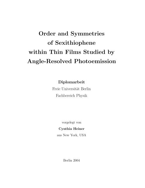
Order and Symmetries<br />
of Sexithiophene<br />
within Thin Films Studied by<br />
Angle-Resolved Photoemission<br />
Diplomarbeit<br />
Freie Universität Berlin<br />
Fachbereich Physik<br />
vorgelegt von<br />
Cynthia Heiner<br />
aus New York, USA<br />
Berlin 2004
Gutachter dieser Arbeit:<br />
Prof. Dr. I. V. Hertel<br />
Die Arbeit wurde durchgeführt am<br />
<strong>Max</strong>-<strong>Born</strong>-<strong>Institut</strong> für Nichtlineare Optik und Kurzzeitspektroskopie Berlin
Abstract<br />
The present work is concerned with the electronic structure and molecular orientation of<br />
thin films of <strong>sexithiophene</strong> (6T), a technologically promising organic conjugated molecule.<br />
Using a Au(110) single crystal substrate to tailor a well-controlled initial self-assembly of the<br />
6T molecules (long axis) along the troughs, well-ordered 6T thin films were grown and maintained<br />
up to ca. 2000 Å. Angle-resolved photoemission from these films, performed at the<br />
<strong>MBI</strong> undulator beamline at BESSY, show a strong intensity dependency on the experimental<br />
geometry. For the present experiments it was, however, necessary to use simultaneous laser<br />
irradiation to compensate for film charging, in order to obtain sharp (and resolved) spectral<br />
features. Additionally, quantum chemical calculations were performed on various simulated<br />
6T isomers (conformers) to compare molecular potential and orbital binding energies. Then<br />
by interpreting the data through symmetry selection rules, the molecules’s relative orientation<br />
was inferred in conjunction with the various molecular orbital character possibilities.<br />
The results firmly suggest the need for alternative molecular symmetries at the surface of the<br />
film as compared to the bulk crystalline structure, namely C 2v and C s vs C 2h , respectively.
Contents<br />
1 Introduction 3<br />
2 General Background 6<br />
2.1 Fundamental Aspects of Photoemission . . . . . . . . . . . . . . . . . . . . . 6<br />
2.2 Synchrotron Radiation from Insertion Devices . . . . . . . . . . . . . . . . . 11<br />
2.3 Thiophene Molecules . . . . . . . . . . . . . . . . . . . . . . . . . . . . . . . 13<br />
2.4 Symmetry Point Groups Relevant for 6T Thin Films . . . . . . . . . . . . . 17<br />
2.5 Hartree-Fock Model . . . . . . . . . . . . . . . . . . . . . . . . . . . . . . . . 22<br />
3 Experimental 27<br />
3.1 <strong>MBI</strong>-BESSY Beamline . . . . . . . . . . . . . . . . . . . . . . . . . . . . . . 27<br />
3.2 UHV Apparatus . . . . . . . . . . . . . . . . . . . . . . . . . . . . . . . . . . 30<br />
3.3 Materials and Film Preparation . . . . . . . . . . . . . . . . . . . . . . . . . 33<br />
4 Results and Discussion 35<br />
4.1 6T Film Characterization: Growth pattern, Thickness, and Morphology . . . 35<br />
4.1.1 Low Energy Electron Spectroscopy (LEED) . . . . . . . . . . . . . . 35<br />
4.1.2 Atomic Force Microscopy (AFM) . . . . . . . . . . . . . . . . . . . . 41<br />
4.1.3 X-Ray Photoelectron Spectroscopy (XPS) . . . . . . . . . . . . . . . 44<br />
4.2 Photoemission Spectra and the Need for Laser Excitation . . . . . . . . . . . 47<br />
4.2.1 6T Spectral Evolution and Assignment Through Coverage . . . . . . 47<br />
4.2.2 Film Charge Compensation in the Presence of Laser Irradiation . . . 51<br />
4.3 Angle-Resolved Photoemission from 6T/Au(110): Molecular Orientation . . 56<br />
4.3.1 Measured Photoemission Anisotropy . . . . . . . . . . . . . . . . . . 56
CONTENTS 2<br />
4.3.2 Calculated Molecular Orbitals: Binding Energies, Characters, and<br />
Symmetries . . . . . . . . . . . . . . . . . . . . . . . . . . . . . . . . 60<br />
4.3.3 Photoemission Data and Computation Comparison . . . . . . . . . . 70<br />
5 Conclusions 79<br />
6 Appendix 81<br />
6.1 Laser Systems Used in Combination with Synchrotron Light . . . . . . . . . 81<br />
List of Figures 83<br />
List of Tables 86<br />
Bibliography 87
Chapter 1<br />
Introduction<br />
In recent years investigations on systems of π-conjugated organic materials, both polymers<br />
and oligomers, have attracted quite a bit of attention owing to their prospects for new technological<br />
applications and devices, and their interesting physical properties. Among these are<br />
particularly polythiophene and its n-thiophene derivatives [1], which have a promising value<br />
for both photonics, including e.g. organic field-effect transistors (OFET) [2], lightweight batteries,<br />
electrochromic devices [3], and optoelectronics, such as organic light-emitting dio<strong>des</strong><br />
(OLED) [4], fast optical switches [5], and solar cells [6]. Of course, to realize the full potential<br />
applications (and device performance) in these electronic or optical devices, it is necessary<br />
to have a good understanding of both the electronic structure and physical properties of<br />
the system. The latter not only depends on the physical properties of the individual organic<br />
molecules but also on their relative orientation, which in turn affects their mutual<br />
interaction and thus fundamental film properties, e.g. charge transfer processes and various<br />
relaxation mechanisms. Thus the creation of highly-ordered organic thin films becomes a<br />
very compelling topic to study.<br />
Sexithiophene, which is the subject of the present study, was originally investigated as<br />
a model system to better <strong>des</strong>cribe its parent 1 , polythiophene [7]. Sexithiophene, 6T, is a<br />
planar, aromatic organic molecule consisting of six conjugated thiophene rings - each ring<br />
1 Well defined (and then highly-ordered) films of polythiophenes are very difficult to achieve, in part<br />
because within the polymerization process, the polythiophenes are likely to develop chemical and/or morphological<br />
defects, e.g. intermolecular entanglements and chain twists, causing break in the electronic conjugation.<br />
This fractioning leads to an assortment of conjugation lengths within the already non-crystalline<br />
(amorphous) polymer structure [11], [12], [13], [14].
4<br />
possesses four carbon atoms and one sulfur atom. After some initial studies on 6T, however,<br />
it became quickly clear that the molecule itself was interesting in that the material (films)<br />
could be well controlled and prospectively tailored (chemical structure changes such as side<br />
or end substitution [7], [8]) for technological applications. In fact, 6T has since been already<br />
used for fabricating devices [9]. Specifically, good control over 6T thin film morphology can be<br />
practically achieved through convenient processing techniques, most commonly using vacuum<br />
sublimation under ultra-high vacuum (UHV) conditions [7]. Clearly the interfacial (organic<br />
film - substrate) properties are also crucial; using UHV is an advantageous technique here<br />
since it assures that no contaminants could interrupt the relationship between the deposited<br />
molecules and the substrate [10]. This provi<strong>des</strong> for suitable control of the interface; for our<br />
purposes this is of particular importance since the substrate serves as a seed to induce a high<br />
structural order to be built up from submonolayer coverage to thin films. This opens the<br />
way to a variety of surface science techniques, some of which are applied within this work<br />
to characterize the 6T film growth.<br />
In the present work the electronic structure of highly oriented <strong>sexithiophene</strong> is studied<br />
using angle-resolved photoemission. The main goal of this study is to infer the structural<br />
and electronic information through symmetries and binding energies, respectively, of 6T<br />
molecules within well ordered thin films. Films were grown on a (1x2)-Au(110) singlecrystal<br />
surface providing a suitable ordered template for highly-orientated molecular (film)<br />
growth. The molecules prefer to nucleate with their long molecular axes along the [110]<br />
direction of the single crystal substrate. Continual deposition of 6T leads to island formation;<br />
however, these islands still posses the same aforementioned preferred orientation within the<br />
macroscopic film. This structure leads to a highly anisotropic emission of photoelectrons.<br />
Presented here are valence band photoemission spectra of thin, well-ordered <strong>sexithiophene</strong><br />
films grown on Au(110) obtained, for 50 eV photon energy, at the <strong>MBI</strong>-BESSY Undulator<br />
beamline (SGM-U125). We were able to compensate for the large amount of synchrotron<br />
induced film charging, typical for low-conducting organic films, by employing simultaneous<br />
laser irradiation. This was necessary, since only in the presence of laser pulses will the<br />
resulting spectra posses sharp features. Furthermore, we show through angle-resolved photoemission<br />
a strong variation of photoemission intensity as a function of the experimental
5<br />
geometry, i.e. the direction of the polarization vector of the incoming excitation-light, and<br />
the angle of photoelectron detection.<br />
The main goal of this latter series of experiments is to indicate the 6T molecular orientation.<br />
This is inferred by applying group theory and symmetry-derived selection rules directly<br />
to the angle-resolved PE data, to examine the permission of detection of photoemitted electrons<br />
from 6T films. By performing parallel quantum-chemical calculations on simulated<br />
(optimized) molecular isomers (conformers), we determined the correlating (molecular orbital)<br />
binding energies, and their respective symmetries, as depending on various 6T molecular<br />
symmetries. The molecules’ resulting relative orientation, after taking into account the<br />
differences between experimental and theoretical frameworks, is discussed in relation to these<br />
various conformers. Notice that photoemission, for photon energies of 50 eV, is a reasonably<br />
surface sensitive technique. Our results suggest a different molecular orientation found at<br />
the surface as compared with previously reported 6T’s bulk-crystalline structure.
Chapter 2<br />
General Background<br />
The main experimental technique applied within the present work, photoemission (PE), will<br />
be briefly revisited (Sec. 2.1). Other techniques used, e.g. Low Energy Electron Diffraction<br />
(LEED) and Atomic Force Microscopy (AFM), will not be <strong>des</strong>cribed here explicitly. Also<br />
included is a general <strong>des</strong>cription of synchrotron radiation (SR) obtained from an undulator<br />
(Sec. 2.2), since the majority of PE experiments were obtained using SR light. Presented in<br />
Sec. 2.3 is an overview of <strong>sexithiophene</strong>’s chemical and physical (electronic) properties, with<br />
an emphasis on the condensed phase. Additionally, a short summary of important aspects<br />
of aromatic organic molecules, specifically n-thiophenes, and their interactions (bonding)<br />
with various metal surfaces for both thin film, sub- and monolayer systems. A particular<br />
focus will be on the molecular orientation within the latter systems. After this general<br />
introduction we will focus on the symmetry details of three reported 6T conformers. This<br />
becomes relevant for interpreting the present PE results by applying group theory, the basics<br />
of which are reviewed in Sec 2.4. Lastly, the theoretical model employed here for binding<br />
energy calculations - the Hartree-Fock model including the basis set 6-31G(d,p) used here -<br />
will be discussed (Sec. 2.5).<br />
2.1 Fundamental Aspects of Photoemission<br />
One of matters’ basic characteristics is that of its electronic structure. This is most commonly<br />
probed by invoking the photoelectric effect [15] in the experimental technique of<br />
photoelectron spectroscopy (PES). Essentially, using photons with a known energy (hν) to<br />
excite a system, emitted electrons can be detected and analyzed according to their respective
2.1 Fundamental Aspects of Photoemission 7<br />
kinetic energy to yield direct individual electronic state information. To guarantee a known<br />
(precise) incoming energy, highly monochromized light is wanted and can be fully exploited<br />
by synchrotron radiation providing photons ranging from the near-ultraviolet (UV) to far<br />
x-ray regimes. The former technique is then called UV Photoelectron Spectroscopy (UPS)<br />
and the latter either X-ray Photoemission Spectroscopy (XPS) or Electron Spectroscopy for<br />
Chemical Analysis (ESCA). This technique can be performed on atoms and molecules in<br />
gas, solid, and liquid phases; however, it should be noted that special technical requirements<br />
are necessary for PES from highly volatile liquids 1 , which have been achieved and detailed<br />
elsewhere [16].<br />
There are two main interpretations of the photoemission process in solids. The simple<br />
so-called three-step model breaks the process up into three distinct stages [17], [18], [19].<br />
First the local absorption of a photon excites an electron. Next the excited electron must<br />
travel through the sample medium to the surface, until it reaches the third step; its escape<br />
into the vacuum where it is detected. Inherently these three steps would be dependent upon<br />
each other and also on the other N electrons within the system; therefore this model is a<br />
somewhat naive and artificial picture of the photoemission process. Thus, a one-step model<br />
is a better theoretical approach, albeit more rigorous.<br />
The absorption of a photon of energy (hν) by an initial system of N electrons, which is<br />
<strong>des</strong>cribed by ψ i (N) and E i (N), will optically excite an electron (possibly photoionization).<br />
After photoionization, the system can be <strong>des</strong>cribed by its remaining N-1 electrons, in a final<br />
state of ψ f (N-1, k) and E f (N-1, k) and the missing electron; k depicts the initial energy<br />
level from which the electron was removed. Here the escaped electron will carry information<br />
of its binding energy, via its kinetic energy E kin [17]. Energy conservation then renders this<br />
relation as<br />
E i (N) + hν = E f (N − 1, k) + E kin (2.1)<br />
This can be re-arranged to show the binding energy with respect to the vacuum:<br />
E B (k) = E f (N − 1, k) − E i (N) (2.2)<br />
To reiterate, the final state wave function is that of an atom with a (positive) hole in level<br />
1 Special parameters must be considered to overcome the difficulties of operating a liquid system in ultra<br />
high vacuum conditions (required for photoemission spectroscopy.)
2.1 Fundamental Aspects of Photoemission 8<br />
nucleus<br />
inner levels<br />
valence band<br />
hν<br />
hν<br />
hν<br />
binding energy<br />
E B = hν - E kin<br />
kinetic energy<br />
of photoelectrons, E kin<br />
E = 0<br />
Fig. 2.1: Illustration of photoemission spectroscopy [20]. Here the initial shell (density of states)<br />
where the electron arises from is shown as dashed lines. These electrons are excited by the incoming<br />
energy hν, which is the difference between the electrons’ binding and kinetic energies.<br />
k. Figure 2.1 visually relates the above equations to the observations made in photoemission<br />
spectroscopy [20].<br />
First we will assume that after the photoionization process the remaining N-1 electrons in<br />
the excited ion, and the N electrons in its neighboring atoms do not re-arrange to compensate<br />
for the electrical imbalance left behind by the escaped electron. This would be more accurate<br />
however, in examining an infinite isolated atomic or molecular system. In such a case one<br />
would say that the identical wave function <strong>des</strong>cribes both the initial, ψ i (N), and final, ψ f (N-<br />
1, k), states, which then <strong>des</strong>cribes the orbitals by the frozen orbital approximation. Within<br />
the Hartree-Fock approximation this leads to Koopmans’ theory - that the binding energy<br />
is the same as the negative orbital energy of the emitted electron (ε k ) [21]:<br />
E B (k) = −(ε k ) (2.3)<br />
This assumption - that the ejection of a photoelectron is much faster than the time needed<br />
for the systems’ valence electrons to re-arrange their charge distribution - encompasses the<br />
appropriately named sudden approximation [18], [19].<br />
However, in the other scenario of the more realistic non-isolated system there is a (fast)<br />
response to the new electronic environment by the remaining N-1 charges; they try to readjust<br />
in such a way as to minimize their energy (relaxation). This relaxation process is then a final<br />
state effect resulting in an extra positive energy value (E R ), which must be incorporated into
2.1 Fundamental Aspects of Photoemission 9<br />
equation 2.3 to correctly evaluate the initial state binding energy [17]:<br />
E B (k) = −(ε k ) − E R (k) (2.4)<br />
Now there is a clear difference between the initial and final wave functions, which has been<br />
appropriately taken into account. This assumption - in which the photoelectron leaves the<br />
system slowly enough that the electrons from or near the excited atom change their energy<br />
by adjusting to the effective atomic potential in a self-consistent way (embodied by E R ) - is<br />
referred to as the adiabatic approximation.<br />
It is important to note at this time that the interactions between the remaining electrons<br />
after ionization are very fast, and a universal agreement for an ”instantaneous” time-scale<br />
is difficult to define. The transition probability, again, depends on the wave functions; thus<br />
it is crucial to know if one has the same or dissimilar initial and final states, or essentially<br />
when to apply which aforementioned approximation(s). There are no strict criteria for the<br />
favored applicability of one approximation over the other in certain defined energy ranges.<br />
The time for the PE process depends on the velocity of the escaping electron and thus<br />
the sudden limit corresponds to high excitation energies. The sudden approximation only<br />
becomes exact in the limit when the photoelectron’s kinetic energy is infinite, as was reviewed<br />
here for an isolated system. Furthermore, the adiabatic approximation, which considers a<br />
photoelectron leaving the system slowly, corresponds to low excitation energies.<br />
Both theoretical and experimental investigations devoted to the estimation of the kinetic<br />
energy limit between the two approximations are not yet entirely conclusive. Results from<br />
Hedin and Johansson [22] are recommended for the more in-depth reader. It provi<strong>des</strong> details<br />
concerning the transition between the approximations and examples of order of magnitu<strong>des</strong><br />
for sp-metals. Other studies and calculations by Gelius [23], applying an optimized Hartree-<br />
Fock-Slater method, breaks the PE process into inter-, intra-, and extra-atomic relaxations.<br />
As previously <strong>des</strong>cribed, the photoemission process is essentially the excitation of an<br />
electron from an initial state to a final state. This excitation is triggered by an electromagnetic<br />
field (UV/X-ray) whose interaction with the initial and final wave functions is the<br />
intensity of the measured PE signal (photocurrent). Describing the system’s ground state<br />
by the Hamiltonian H 0 and the ionizing photon beam as H’, the transition probability per
2.1 Fundamental Aspects of Photoemission 10<br />
unit time between the two eigenstates ψ i and ψ f is given by Fermi’s Golden Rule [18]<br />
R = 2π¯h |〈Ψ f|H ′ |Ψ i 〉| 2 δ(E f − E i − ¯hω). (2.5)<br />
The perturbation (using the first-order perturbation theory [24]) is then expressed by [17]<br />
H ′ =<br />
e · (Ap + pA), (2.6)<br />
2mc<br />
where P is given by the momentum operator -ih∇ and A being a plane wave, A(r,t)=A 0 exp(-<br />
iωt+iqr), <strong>des</strong>cribing the vector potential of the incident light. This operator equation can<br />
be reduced, by involving the dipole approximation [20], [24], to form a final perturbation of<br />
H ′ = −→ E · −→ µ (2.7)<br />
Within the approximation the vector potential A collapses an electric field −→ E , and −→ µ is<br />
the dipole moment 2 .<br />
Also, it is important to note that UPS is a reasonably surface sensitive technique [25].<br />
In handling the complex, interconnected system of atoms (i.e. a non-isolated case such as a<br />
solid), the strong interactions of the electrons with matter must be taken into account. An<br />
electron travelling through a solid has a specific probability of escaping into vacuum without<br />
any inelastic scattering events causing the electron to suffer energy losses. Only electrons<br />
that escape from the solid collision-free, carry direct information of the electronic structure.<br />
This certain information depth is known as the mean free path or the electron escape depth,<br />
and is a function of the electron kinetic energy.<br />
This relation is known as the universal<br />
mean free path curve 3 , displayed in Fig. 2.2. The minimum of this curve, at ca. 20-100 eV,<br />
refers to the energy range of maximum surface sensitivity (lowest escape depth). The large<br />
number of electrons that originate from distances larger than the electron escape depth (on<br />
the order of a few monolayers) will undergo inelastic scattering events, which results in the<br />
secondary electron background signal in PES.<br />
2 The measured effect here can be also calculated by the application of group theory (see background Sec.<br />
2.2). These two methods have one important factor in common: Altogether the intensity of the photoemission<br />
signal depends on the transition probability given by the initial and final wave functions, determined by the<br />
wave function’s respective character.<br />
3 The quasi-universal behavior of electron mean free path, regardless of material, comes from the major<br />
interaction mechanism between electrons and a solid. That is to say the excitation of plasmons; this is a<br />
fundamental interaction of the electron density of solids, which is very similar in most cases.
2.2 Synchrotron Radiation from Insertion Devices 11<br />
1000<br />
mean free path [monolayers]<br />
100<br />
10<br />
1<br />
1 10 100 1000<br />
kinetic energy [eV]<br />
Fig. 2.2: The universal mean free path of electrons [17], referring to the the electron escape depth<br />
in solids, as a function of kinetic energy.<br />
2.2 Synchrotron Radiation from Insertion Devices<br />
A brief look at the advantages of synchrotron radiation (SR), as the photon source of most<br />
of the present PE measurements, and how it is of particular use related to this work will<br />
be reviewed. This is admittedly not only non-exhaustive but presented with a very narrow<br />
scope pertaining only to the present experiments performed with undulator radiation.<br />
Synchrotron radiation is emitted when charged relativistic particles, electrons for instance,<br />
are subjected to centripetal acceleration. In a synchrotron, accelerated electrons are<br />
forced into a circular orbit by magnetic fields 4 . These relativistic electrons (v/c = β ≈ 1)<br />
radiate light tangentially to their orbit (in the forward direction) in a narrow cone [18]. The<br />
higher the kinetic energy of the electrons the narrower the emission cone becomes, while<br />
likewise extending the spectrum of the emitted radiation to higher energies. The spectral<br />
intensity of synchrotron radiation is characterized by its brilliance [24]<br />
B =<br />
spectral flux into 0.1% bandwidth<br />
source area (mm 2 ) · solid angle (mrad 2 ) · 100(mA) . (2.8)<br />
A further important feature of synchrotron radiation is its linear polarization, which is the<br />
key property for the present experiments. 3 rd generation synchrotron facilities use insertion<br />
devices (undulators or wigglers) - magnetic arrays (N periods with period length λ 0 ) within<br />
the straight sections of the storage ring - to achieve much higher brilliance as compared<br />
4 The word ”synchrotron” evolved from the idea of synchronization of magnetic fields and photon energy.
2.2 Synchrotron Radiation from Insertion Devices 12<br />
Fig. 2.3: Schematic of the magnetic structure of a wiggler/undulator [26]. The distance between<br />
the magnets (gap) is labelled as h. Here the electrons’ propagation is along the z-direction (planar)<br />
and its oscillation within the x-z plane. Radiation is emitted (in the forward direction) at each<br />
curve; the total of these individual intensities increases with the number of poles in the electron<br />
path.<br />
to simple bending magnets. The magnetic structure of a wiggler/undulator 5 is shown in<br />
Figure 2.3. Specifically, for an undulator defined by a characteristic K (≈ 0.934B 0 λ 0 ≈ 1)<br />
parameter, which is not further detailed here (see [24]), light emitted from each individual<br />
periodic magnetic structure adds up coherently 6 . This causes the spectral intensity to be<br />
confined around a certain wavelength (quasi-monochromatic) at highly increased brightness<br />
(see [24]). The wavelength of the radiation can be adjusted by the magnetic field strength, B 0 ,<br />
of the device, which is performed by changing the distance between the magnet poles, referred<br />
to as changing the undulator gap. For a planar undulator the light is linearly polarized,<br />
in the direction of the oscillations of the electrons’ trajectories; circularly or elliptically<br />
polarized light can be generated by specially arranged magnetic structures. Finally, modern<br />
synchrotron sources typically deliver pulse widths of only 30-50 ps 7 , which can be directly<br />
used for time-resolved experiments. A special application is the combination of short laser<br />
and synchrotron pulses in a pump-probe experiment as addressed in Sec. 6.<br />
5 Undulators and wigglers are in principle the same; they differ in the magnetic field values - e.g. wigglers<br />
produce higher magnetic fields but have fewer magnetic poles than undulators.<br />
6 Constructive interference results from the overlap of the light cones of the individual wiggles and electromagnetic<br />
waves emitted from the same electron at different positions as it passes through the magnetic<br />
structure.<br />
7 Even smaller pulse widths, ∼ 1 ps, are also available in the low-α mode [27]
2.3 Thiophene Molecules 13<br />
2.3 Thiophene Molecules<br />
This section is intended to give an introduction to the molecular architecture of oligothiophenes<br />
(OT). Additionally, an overview on the molecules’ interactions with particular<br />
substrates, specifically Au (since this substrate was used for the present experiments), and<br />
the implications of these interactions with respect to the molecules’ orientation in the monolayer<br />
regime and in multilayer films is presented. Optical and electronic properties are only<br />
touched upon here, since the electron energies of 6T are investigated in further detail in Sec.<br />
4.3.2.<br />
Thiophene is a five-membered sulfur-containing aromatic compound, as sketched in Figure<br />
2.4. The addition of adjacent monomer units, each bonded via the α-carbons - i.e. the<br />
carbons neighboring the sulfur atoms [28] - results in oligomers (small chain length polymers)<br />
of thiophene (nT). In our case, we have a chain of six thiophene monomers. The two carbon<br />
atoms opposite of the sulfur, known as β-carbons [29], [30], are not affected by the chain<br />
length (since they do not directly interact, e.g. in a bridge position, with the neighboring<br />
rings). Thiophene rings can be conjugated as cisoid (all sulfur atoms on the same side, then<br />
all-cis) or transoid (all alternating, then all-trans); these gas-phase conformations differ by<br />
180 ◦ dihedral (torsion) angle, and are very similar in energy (see Sec. 4.3.2). The situation<br />
may be different for adsorbed molecules, where this small energy barrier [31], [32] may be<br />
overcome by involving the carbon and sulfur atoms in surface bonding [6].<br />
It is exactly<br />
this surface-bonding mechanism, which varies depending on substrate, that determines the<br />
orientation of the seeding monolayers, and is thus crucial for the formation of long-range<br />
ordered multilayers of OTs (and other large organic molecules) on crystalline surfaces.<br />
Metal substrates are then appreciable templates as they may provide considerable covalent<br />
interactions 8 with the organic molecule, and particularly the lateral ordering, at least<br />
in the monolayer regime, results from the interplay of both the substrate-adsorbate and the<br />
adsorbate-adsorbate interactions [33]. (These interactions may also result in different molecular<br />
isomers being found in the film than those expected (energetically favored) in the gas<br />
8 The bonding mechanism between nT’s and metals (noble and transition) is generally accepted to strongly<br />
involve the substrate d bands with a charge transfer from the molecular π-states to these d-bands, with an<br />
(almost) simultaneous back donation to the π ∗ states of the molecule [34].
2.3 Thiophene Molecules 14<br />
S<br />
H<br />
C α<br />
C α<br />
H<br />
C β<br />
H H<br />
6<br />
Fig. 2.4: Sketch of a thiophene monomer with the atomic nomenclature for the carbon atoms.<br />
Sexithiophene consists of six conjugated rings.<br />
C β<br />
phase; this is something that will be thoroughly addressed in the present work (Sec. 4.3.2-3).)<br />
Finally, in most cases, this balance of interactions leads to commensurate superstructures<br />
for the first organic monolayers. Additionally, nT’s were found to adsorb nondissociatively<br />
on many noble metal surfaces; in fact the bonded molecules still exhibit sufficient lateral<br />
mobility for two-dimensional ordering. Mobility only, however, doesn’t necessarily warrant<br />
the formation of an ordered adsorbate monolayer. The substrate must additionally act as<br />
a template, e.g. through a particular corrugation structure that forces the assembly of the<br />
overlayer. Furthermore, any degree of order also sensitively depends on the experimental<br />
parameters (e.g. deposition rate [35]).<br />
Specifically on the Au and Ag single-crystal surfaces, the molecules tend to adsorb in a<br />
coplanar geometry (ring planes parallel to the surface); this is attributed to a preferential<br />
bonding to the metal via the conjugated π-system 9 [33], [36].<br />
Parallel geometry is often<br />
taken as an indication of bonding via the ring π-electrons 10 , which may be identified in<br />
photoemission by peak shifts of the π-orbital features, or differential shifts of the σ-features,<br />
toward higher binding energies (see also Sec. 4.2.1). This so-called π-stabilization is a general<br />
feature of π bonding of aromatic molecules to metallic surfaces. In fact, although nT’s have<br />
been studied on various substrates (not only metallic), the question of chemical interactions,<br />
and likewise of other bonding mechanisms, is still highly debated 11 .<br />
9 The sulfur electrons play no important role in bonding [36].<br />
10 A parallel geometry does not necessarily define π-stabilization. Both benzene and bithiophene on Al(111)<br />
adopt a flat-lying geomerty, however, they are bonded via a purely electrostatic mechanism (no bonding of<br />
either the π-electrons or the S lone pair) [28], [34].<br />
11 For example, 4T on Ag(111) has been reported to have a weak coupling [36] but also a covalent<br />
(chemisorptive) [33] bonding character. Also, on Ni(110) and Cu(110) strong π-bonding is observed, which<br />
can then be de-activated, in both cases, by a sulfur-modification (passivation) of the surface [30]. However, a
2.3 Thiophene Molecules 15<br />
a<br />
a<br />
b<br />
c<br />
b<br />
c<br />
Fig. 2.5: Stereographic view of the 6T unit cell, as inferred from x-ray diffraction measurements.<br />
This herringbone packing structure is very common among planar organic molecules [41].<br />
Even for the present system, 6T/Au(110), theory and experiment are in disagreement<br />
as to the bonding mechanisms at the Au-nT interface 12 [37], [38], varying between strong<br />
π-bonding to weak electrostatic interactions (similar strength to Van-der-Waals) - we will<br />
detail this in Sec. 4.2.1. Yet, the 6T overlayer on this substrate has been shown to act as a<br />
template for the planar and orientationally ordered growth of at least five monolayers [39].<br />
However, reasonable order can still be maintained for films as thick as ca. 2000 Å, which is<br />
one of the focuses of the present work.<br />
In the solid state (and thin films), nT molecules (n > 3) are almost planar (small tilt<br />
angle), with the point group symmetry C 2h for even numbered oligomers or C 2v for odd<br />
numbered oligomers [29]. 6T molecules usually crystallize in a herringbone (HB) structure,<br />
common to planar molecules, in which the molecules face each other forming a quasi bidimensional<br />
H frame [40]. The unit cell for crystalline 6T is presented in Figure 2.5 [41].<br />
Another helpful illustration of the 6T HB structure is presented in Figure 2.6 as shown<br />
through space-filling molecular orbitals [42]. Orientational disorders of the molecules in the<br />
HB lattice were shown to strongly affect the crystals’ optical and electronic properties [40]<br />
(quenching optical signal and breaking the π-electron system). Hence it is <strong>des</strong>irable to have<br />
further S-modification (from a c(2x2)S and p(4x1)S surface) posses a still more reactive surface bonding [6].<br />
12 It is worthy to note that this nT-substrate interaction, even when being a weak interaction, is still<br />
proposed to be responsible for the likely reconstruction of the substrate atoms, specifically for Au(110) and<br />
Al(111) surfaces [28], [34], [39].
2.3 Thiophene Molecules 16<br />
20.00 Ångstroms<br />
Fig. 2.6: Space filling sketch of the herringbone pattern of the crystallized 6T lattice packing [42].<br />
control of the arrangement of molecules (not only at the interface), which would affect their<br />
mutual distance and thus their interactions, within a thin film (solid) sample. Again, this<br />
intimately depends on the experimental parameters.<br />
Lastly, a brief look at the optical and electrical properties of 6T. The optical absorption<br />
spectrum of a thin film (ca. 50 nm) 6T/quartz 13 is presented in Figure 2.7. Since laser irradiation<br />
is used within this work to compensate for film charging (Sec. 4.2), the Ti:sapphire<br />
wavelength (second harmonic) is marked in the figure to guide the reader’s eye. Note that<br />
the absorption at λ = 400 nm lies in the middle of an absorption plateau, stretching between<br />
ca. 370 - 460 nm. It is worth mentioning that this absorption spectrum corresponds well<br />
with those found in literature [1], [43], [44]. Moreover, the electronic structure of 6T, particularly<br />
the π-orbitals (these are the orbitals important in surface chemical bonding), consists<br />
of a pair of localized and delocalized molecular orbitals per thiophene ring 14 (bonding and<br />
anti-bonding, see Sec. 2.5) [29], [31]. Here localized and delocalized refer to the probability<br />
of locating the electron wavefunction anchored on one atom (localized) or free to roam<br />
among several neighboring atoms (delocalized), specifically the carbon atoms. For the sp<br />
hybridized carbon atoms within 6T, there exists three σ-bonds and one remaining p-orbital,<br />
which overlaps with the adjoining unsaturated p-atomic orbital to form the continuous π-<br />
network (hence the term conjugated polymer) [45]. Figure 2.8 visually depicts the delocalized<br />
and localized orbitals, in 2-D and 3-D on the left and right si<strong>des</strong> respectively, according to<br />
13 Film was grown under identical deposition parameters as those grown on Au(110), which were used in<br />
the present experiments.<br />
14 The valence orbitals develop gradually from molecular orbitals into broad bands in the large length<br />
limit [31].
2.4 Symmetry Point Groups Relevant for 6T Thin Films 17<br />
0,7<br />
0,6<br />
223<br />
ca. 50nm 6T/Quartz<br />
Absorbance [arb. units]<br />
0,5<br />
0,4<br />
0,3<br />
0,2<br />
0,1<br />
277<br />
366<br />
de-charging<br />
laser<br />
448<br />
474<br />
517<br />
0,0<br />
200 300 400 500 600<br />
Wavelength [nm]<br />
Fig. 2.7: Absorption spectrum of thin film of 6T on Quartz. The first excitation band inclu<strong>des</strong><br />
four peaks; the wavelength of the de-charging laser (marked) lies in the middle of this band.<br />
the location of the carbon double and single bonds 15 . Notice that when the electronic structure<br />
consists of carbon double bonds connecting the C α -C β (top-left) the π-electron system<br />
likewise extends between the rings (top-right). This is known as aromatic character; clearly<br />
here no contribution stems from the sulfur atom. When the sulfur p z orbital does participate<br />
in the molecular orbital (bottom-right), it remains separate from the delocalized carbon<br />
bonds, the C β -C β double bond (bottom-left) - i.e. localizing the electrons to one thiophene<br />
unit. This is denoted as quinoid character, always with significant electron density on the<br />
sulfur and (almost) no density on the C α ’s.<br />
2.4 Symmetry Point Groups Relevant for 6T Thin Films<br />
Within the scope of this work group theory will be applied, in the form of selection rules, to<br />
examine the permission of detection of photoemitted electrons from 6T films. The selection<br />
rules are based on the innate symmetries of the molecule.<br />
It is important to note that<br />
symmetries may be different for molecules adsorbed at a single-crystal substrate vs the<br />
multilayer/vacuum interface. A small review of the implications driven by symmetries will be<br />
presented here; for a more in-depth look into this topic the reader is referred to [46], [47], [48].<br />
15 The backbone of this structure (alternating double and single carbon bonds) resembles that of polyacetylene,<br />
a model organic molecule, however, with the sulfur atom breaking the symmetry [31].
2.4 Symmetry Point Groups Relevant for 6T Thin Films 18<br />
S<br />
S<br />
aromatic<br />
(delocalized)<br />
quinoid<br />
(localized)<br />
S<br />
S<br />
Fig. 2.8: The two types of molecular orbital characters for thiophenes: aromatic vs quinoid. The<br />
particular pattern of the carbon double and single bonds dictate the localization of the orbitals’<br />
π-electrons.<br />
Molecules themselves have innate symmetry elements, such as mirror planes or rotational<br />
axes, which likewise applies to the electronic wave functions (orbitals). An operation that<br />
moves the entire molecule into a new position that is identical to its original one is known<br />
as a symmetry operator.<br />
There are four symmetry operators pertinent to this work: the rotation of a molecule<br />
about any fixed axis, C, with a rotation angle, 2π/n, leads to the expression C n . A reflection<br />
through a plane (mirror symmetry) is denoted by σ; in our case σ may carry a subscript of<br />
either v or h to indicate a vertical or horizontal plane, respectively. An inversion, i, takes<br />
each atom of a molecule and passes it through the molecule’s center to affix it on to the<br />
opposite side of the molecule. Lastly the identity - wherein essentially nothing happens to<br />
the molecule - would, of course, produce an identical image; this is marked by either E or I.<br />
All molecules can be filed according to their symmetry elements into point groups that fulfill<br />
the highest number of symmetry operations (wherein the operators are already manipulated<br />
into mathematical groups 16 ).<br />
Here is a quick familiarization for the point groups addressed throughout this work.<br />
Although C 1 is officially a point group it actually defines a molecule with no symmetry.<br />
16 Any mathematical group possesses four basic properties: the existence of an identity and an inverse<br />
(reciprocal), the associative property between any two operators, and that the product of any two operators<br />
results in an operator contained within the group.
2.4 Symmetry Point Groups Relevant for 6T Thin Films 19<br />
C 2<br />
axis<br />
Highest symmetries<br />
C 2<br />
axis<br />
C 2v<br />
C 2h<br />
σ v<br />
Reduced symmetries<br />
C 2<br />
axis<br />
σ h<br />
C s<br />
C 2<br />
σ h<br />
No symmetry<br />
C 1<br />
Fig. 2.9: Oligothiophenes isomers belonging to the various symmetry point groups pertinent to<br />
this work. The higher symmetry groups are shown (top) as well as each of these (C 2h and C 2v )<br />
symmetry reductions, possessing a broken horizontal or vertical mirror plane, respectively.<br />
Often such a situation arises for a molecule that initially possesses a higher symmetry but is<br />
deformed, for example a bent or broken molecule, and must reduce its symmetry to C 1 . The<br />
next two symmetries, C s and C n , are also common symmetry reductions. They each contain<br />
only one symmetry operator that leaves the molecule invariant, namely a plane of reflection<br />
for C s and an n-fold axis of rotation for C n . The most complex symmetries investigated<br />
here, albeit still relatively low symmetries, are C nv and C nh , which contain both mirror and<br />
rotational symmetries. C nv can only have vertical mirror planes that are situated collinear to<br />
the rotation axis whereas C nh maintains only horizontal mirror planes that are perpendicular<br />
to the C n axis. For our purposes the rotational angle around the C n axis will always be 180 ◦<br />
degree so it will be further referred to simply as the C 2 axis.<br />
All of these symmetries, possessed by oligothiophene isomers, are drawn in Figure 2.9<br />
to aid the reader in visualizing the aforementioned symmetry elements and operators. In<br />
Figure 2.9 the two highest symmetries seen in this work are C 2v and C 2h , shown in the upperleft<br />
and upper-right corners of the sketch, respectively. The C 2v bithiophene will return to an<br />
identical position when rotated into the page of the paper, or around the C 2 axis (red), which<br />
is (and must be) collinear to the one existing vertical reflection plane (σ v ) extending along the<br />
y-z axis. Clearly thiophene rings have only one sulfur atom that has no mirror image across<br />
the molecule’s x-z axis, rendering this plane as a low symmetry axis. The implications of this
2.4 Symmetry Point Groups Relevant for 6T Thin Films 20<br />
will be <strong>des</strong>cribed in the results and discussions (Sec. 4.3.3). Furthermore the constructed C 2h<br />
bithiophene also has a C 2 axis where the rotation of the molecule occurs in the plane of the<br />
page, or the C 2 axis is directed out of the page, and perpendicular to it lies the mirror plane.<br />
This defines a symmetry above and below the molecule itself. Instinctively one notes then<br />
that any slight defect in the linear alignment of the molecule would cause the symmetry<br />
plane to break. If all the rings were twisted out of plane, but twisted congruently by an<br />
exact angle, then there would still be a reduction in symmetry for the entire molecule, but<br />
it would only be to a C 2 symmetry (middle, right). It is worth noting that a C s symmetry<br />
is another possibility (middle,left); this occurs when the molecule remains planar but (1)<br />
one of the rings is ”flipped” (a 180 ◦ degree rotation around the dihedral angle) breaking<br />
the vertical mirror symmetry, or (2) the plane where the molecule exists is tilted at some<br />
angle with respect to a normal coordinate system. This latter symmetry may account for<br />
the herringbone molecular structure observed in bulk 6T (Sec. 2.3). Moreover for 6T, the<br />
C s symmetry can exist for twenty different planar conformers, e.g. with all the rings except<br />
one with identical positioned sulfur atoms. A defect that occurs when the entire molecule<br />
is broken or rearranged into a completely asymmetrical conformation (and probably not<br />
planar) would subject the molecule to a further symmetry reduction to a C 1 point group<br />
(bottom).<br />
Furthermore, all the symmetry operators (within a point group) are conventionally represented<br />
in a matrix form, and within this are the characters reduced into their irreducible<br />
forms. In our cases this refers to a block (square) matrix of sets of (1x1) matrices. Applying<br />
the symmetry operators of any point group, which of course leaves the molecule invariant,<br />
to all molecular orbitals, that is to say the Eigen functions of the symmetry operators, determines<br />
whether the orbital is symmetric or anti-symmetric (with respect to the symmetry<br />
operations). Mathematically speaking this would define<br />
Sψ = ±1ψ, (2.9)<br />
where S is the symmetry operator acting upon the Eigen function ψ, and +1 and -1<br />
represent symmetric and anti-symmetric states, respectively. The (1x1) matrix combinations<br />
from 2.9 can be summarized into character tables. The character tables for the symmetries<br />
reviewed here are shown in Tables 2.1- 2.5.
2.4 Symmetry Point Groups Relevant for 6T Thin Films 21<br />
C 1 I Polarization<br />
A 1 T z , T x , T y<br />
Tab. 2.1: The universal C 1 symmetry character table. In this lowest symmetry emission is always<br />
permitted.<br />
C 2 I C 2 Polarization<br />
A 1 1 T z<br />
B 1 -1 T x , T y<br />
Tab. 2.2: The universal C 2 symmetry character table. This symmetry is generally a symmetry<br />
reduction, due to a main symmetry plane being broken, usually originating from a C 2v or a C 2h<br />
symmetry.<br />
The tables contain three main areas: the names of each irreducible representation (the<br />
letters in the far-left column), the symmetry operations and the resulting character of the<br />
orbitals, symmetric or anti-symmetric (consisting of the bulk of the tables), and the polarization<br />
of the characters (far-right column). The irreducible representations are known as<br />
Mulliken symbols and can be directly derived as traces incorporating all symmetry operators<br />
[46]. The characters A and B, found in all the tables, are one-dimensional and differ<br />
only when being acted on by the principle rotational operation, C 2 , in its symmetric/antisymmetric<br />
character. The C 2h orbital subscripts g and u - originating from the German<br />
words gerade and ungerade meaning even and odd, respectively - refer to the symmetry with<br />
respect to inversion. An inversion operation, where g is symmetric, results from a s- and<br />
d-orbital transformation, p- and f-orbitals produce an anti-symmetric u; more explicitly an<br />
inversion creates a transformation into minus itself. Lastly, the subscripts for C 2v , 1 and 2,<br />
refer to the orbital character being symmetric or anti-symmetric with respect to a reflection<br />
through the (xz)-plane. Likewise, C s orbital superscripts ’ and ” denote the same respective<br />
orbital character, however with respect to the horizontal plane.<br />
C s I σ h Polarization<br />
A’ 1 1 T x , T y<br />
A” 1 -1 T z<br />
Tab. 2.3: The universal C s symmetry character table. This symmetry is generally a symmetry<br />
reduction, due to a main reflection symmetry plane being broken from a C 2v symmetry.
2.5 Hartree-Fock Model 22<br />
C 2h I C 2 i σ h Polarization<br />
A g 1 1 1 1<br />
B g 1 -1 1 -1<br />
A u 1 1 -1 -1 T z<br />
B u 1 -1 -1 1 T x , T y<br />
Tab. 2.4: The universal C 2h symmetry character table. The horizontal plane of symmetry makes<br />
for the identical permission of x and y detection. Where no detectable transmission is listed, the<br />
transition is considered forbidden.<br />
C 2v I C 2 σ v (xz) σ v(yz) ′ Polarization<br />
A 1 1 1 1 1 T z<br />
A 2 1 1 -1 -1<br />
B 1 1 -1 1 -1 T x<br />
B 2 1 -1 -1 1 T y<br />
Tab. 2.5: The universal C 2v character symmetry table.<br />
z-excitations, posses individual selection rules.<br />
Here all three directions, x-, y-, and<br />
2.5 Hartree-Fock Model<br />
Theoretical quantum-chemical calculations combined with the measured PES data are a very<br />
powerful tool in experimental analysis. Not only are the binding energy calculations helpful<br />
in providing a direct correlation to the PE spectra, but they are also beneficial for determining<br />
the symmetries associated with each energy level. In simulating three <strong>sexithiophene</strong><br />
conformers, each manipulated to possess a specific symmetry (see Sec. 2.4), total molecular<br />
potential energies and individual molecular orbital binding energies can be calculated. It is<br />
the symmetries of the latter that is necessary for the application of group theory.<br />
There are a variety of calculation models in use today; the most of which are tailored to<br />
be advantageous for (only) certain situations searching for very particular variables. For our<br />
purposes of optimizing constructed molecules (i.e. parameters such as bond distances, bond<br />
angles and dihedral angles), the Hartree-Fock method was implemented, in which quantum<br />
mechanics <strong>des</strong>cribes the molecular geometry in terms of minimum energy (optimal) arrangements<br />
[49] of the electronic and nuclear charges 17 . We simplify this process by involving<br />
17 Here we consider a general Schrödinger equation, ĤΨ=EΨ, where Ψ is a many-electron wavefunction<br />
and the Hamiltonian, Ĥ, is expressed by:<br />
Ĥ = −h2<br />
nuclei<br />
∑<br />
8π 2<br />
A<br />
1<br />
M A<br />
▽ 2 A− −h2<br />
electrons<br />
∑<br />
8mπ 2<br />
a<br />
nuclei<br />
∑<br />
▽ 2 A−e 2<br />
A<br />
electrons<br />
∑<br />
a<br />
nuclei<br />
Z A<br />
∑<br />
+e 2<br />
r Aa<br />
A><br />
nuclei<br />
∑<br />
B<br />
Z A Z B<br />
R AB<br />
electrons<br />
∑<br />
+e 2<br />
a><br />
electrons<br />
∑<br />
b<br />
1<br />
r ab<br />
(2.10)
2.5 Hartree-Fock Model 23<br />
two approximations, the first of which is the Hartree-Fock approximation.<br />
This involves<br />
replacing the many-electron wave function of the molecular system by a product of<br />
one-electron wavefunctions (spin orbitals). These substitutes are known as Hartree-Fock or<br />
single-determinant wavefunctions. Each spin orbital incorporates a space part (ψ) - function<br />
of the coordinates of a single electron (molecular orbital) - multiplied by a ± 1 2<br />
part (either α or β, respectively). The consequential set of differential equations is then<br />
interpreted by applying the other approximation, the Linear Combination of Atomic<br />
Orbitals (LCAO) approximation. As the name implies, this approximation uses solutions<br />
for the hydrogen atom to produce one-electron solutions for many-electron molecules.<br />
Essentially, albeit over-simplified, this stems from the argument that since molecules consist<br />
of atoms, solutions to molecules would also be comprised of atomic solutions. The employed<br />
molecular orbitals are expressed as a set of linear combinations (basis set) forming the basis<br />
functions (φ)<br />
ψ i =<br />
basisfunctions ∑<br />
µ<br />
spin<br />
c iµ φ µ (2.11)<br />
The LCAO expands equation 2.11, within which φ µ is referred to as an atomic orbital since<br />
it <strong>des</strong>cribes the behavior of an electron that is generally centered around the position of the<br />
nucleus (”center of the atom”), and c is the atomic orbital coefficient.<br />
The combination of these two approximations, when applied to the electronic Schrödinger<br />
equation, yields the Roothaan-Hall equations [49]:<br />
basisfunctions ∑<br />
ν<br />
(F µν − ε i S µν )c iµ = 0 (2.12)<br />
Here, ε is the energy of the orbital, S is the overlap matrix 18 (the interaction of the basis<br />
functions), and F is the Fock matrix (analogous to the Hamiltonian).<br />
The results from<br />
equation 2.12 are collectively termed Hartree-Fock, generally they belong to the class of ab<br />
initio models.<br />
Then applying the <strong>Born</strong>-Oppenheimer Approximation - that the nuclei are fixed in space within the molecular<br />
system - we simplify the above equation by reducing the nuclear kinetic energy (1 st term) to zero and<br />
the nuclear-nuclear Coulomb (4 th term) to a constant. This BO Schrödinger, also known as the ”electronic”<br />
Schrödinger equation, is the starting point for almost all quantum-chemical calculations.<br />
18 The atomic orbital coefficients are required, by symmetry, to be equal. Thus normalizing ψ is as<br />
follows [48]:<br />
∫<br />
∫<br />
∫<br />
1 = ψ ∗ ψ dτ = (c ∗ aa ∗ ± c ∗ ab ∗ )(c a a ± c a b)dτ = 2|c a | 2 ± 2|c a | 2 a ∗ bdτ (2.13)<br />
Now a and b are normalized and real, resulting in the overlap integral; S ab = ∫ a ∗ b dτ.
2.5 Hartree-Fock Model 24<br />
Fig. 2.10: Graphical representation of the bonding (φ g ) and anti-bonding (φ u ) process within the<br />
hydrogen-molecule ion, H + 2 . The systems’ two protons are labelled a and b.<br />
The Hartree-Fock (HF) model employs a basis set that chooses Gaussian-type functions<br />
that are very similar to the solutions to the hydrogen atom [49]. To see the pivotal position<br />
of the LCAO approximation within the HF model, let’s first examine the exact solution for<br />
the hydrogen-molecule ion, H + 2 . In this case two identical 1s wavefunctions, φ a and φ b , each<br />
centered around proton-nuclei a and b, come together to form one wavefunction (ψ), as shown<br />
graphically in Figure 2.10 [20]. The resulting ψ g and ψ u represent the even and uneven mixing<br />
of the φ’s. Although this is a trivial fact, it is important in our studies of binding energy<br />
calculations that the reader be reminded of the fundamental energy differences existing<br />
between even (bonding) and odd (anti-bonding) wavefunctions. The higher stability found<br />
in bonding wavefunctions lowers its total energy level to below that of the independent<br />
φ’s. This is due to the larger probability of charge occupying the central region where it<br />
will enjoy the attractive potentials from both protons. The node in the middle of the antibonding<br />
wavefunction clearly <strong>des</strong>troys such chances, and instead distributes the charge more<br />
toward the outer edges of the molecule, where the electron feels only one nucleus [48]. The<br />
exact energy splitting is dependent upon the distance between the two nuclei, R ab , as shown<br />
in the graph in Figure 2.11 [20].<br />
However, here the experiments were conducted on a molecule containing sulfur and carbon<br />
atoms in addition to hydrogen atoms. So the atomic orbitals (φ) that are being combined<br />
within the LCAO approximation consist of wavefunctions from the 2s (φ s ) and 2p (φ p ) subshells<br />
19 . The φ p function possesses three asymmetrical parts, each aligning itself along the<br />
19 Just to remind the reader, the s-wavefuntions are symmetric with respect to the nucleus whereas p-
2.5 Hartree-Fock Model 25<br />
Fig. 2.11: Graph showing the dependence of the bonding energy, associated with bonding character,<br />
as a function of the distance between nuclei, R ab .<br />
three principle axes, x, y and z, where the nucleus is positioned at the origin.<br />
combination, of φ s and φ px for example, would lead to the new wavefunctions 20<br />
A linear<br />
ψ + = φ s + φ px and ψ − = φ s − φ px (2.14)<br />
A graphical view of these equations is presented in Figure 2.12. In this picture it is clear<br />
to see that by combining the φ s (dashed line) with φ px (dash-dotted line), the resulting φ +<br />
wavefuntion (MO) has shifted its center of charge as compared to the s-function. In other<br />
words, the electronic motion is not centered around the nucleus. The same principle of the<br />
LCAO approximation expressed in Figure 2.12 is represented as a pictorial in Figure 2.13<br />
of the atomic orbitals combination for pd (top) and sp (bottom) hybridization (the latter<br />
hybridization is exactly that plotted in Figure 2.12). Here we see the initial atomic orbital<br />
(φ i ) being added to the λ of the next subshell to show that hybridization (polarized) effects<br />
are still encountered, even when factoring in empty subshells. By taking this polarization into<br />
account, and likewise the dissimilar atomic orbital coefficients (c) that vary with different<br />
atoms, provi<strong>des</strong> for a more accurate <strong>des</strong>cription of the bonding within any molecular system.<br />
Applied in the present study was the well-accepted polarization basis set 6-31G(d,p).<br />
This basis encompasses the aforementioned hybridization, up to the d-subshell, as well as introducing<br />
a split-valence parameter. This parameter essentially inclu<strong>des</strong> two separate terms<br />
to <strong>des</strong>cribe the inner-shell and valence electron distributions. The inner shell (σ) electrons<br />
are all symmetric 21 , and within the 6-31G(d,p) can be grouped together and represented by<br />
wavefunctions are anti-symmetric. These same symmetry arguments can be applied to molecular wavefunctions,<br />
which are then known as σ and π, respectively.<br />
20 This assumption is valid when the 2s and 2p states are degenerate, as is the case in a C-H bond.
2.5 Hartree-Fock Model 26<br />
Fig. 2.12: In this picture it is clear to see that by combining the φ s (dashed line) with φ px<br />
(dash-dotted line) that the resulting φ + wavefuntion has shifted its center of charge as compared<br />
to the s-function.<br />
six Gaussian curves. The valence orbitals are then split into two functions containing one<br />
and three Gaussian curves.<br />
Fig. 2.13: A cartoon showing the polarization effects resulting from including the next subshell<br />
within the confines of LCAO approximation.<br />
21 Although the p-wavefunction is antisymmetric, in -plane p x and p y orbitals combine to form symmetric<br />
wavefunctions. These p orbitals are then also termed ”tight” σ-bonded, to distinguish them from their<br />
p z -orbital counterparts - they are called ”loose” π-bonded.
Chapter 3<br />
Experimental<br />
This section provi<strong>des</strong> a detailed overview of the experimental <strong>des</strong>ign and techniques used<br />
for obtaining the presented data. The experimental setup is separated here into its two<br />
main components: the <strong>MBI</strong>-BESSY beamline (Sec. 3.1) providing the synchrotron radiation,<br />
and the ultra-high vacuum surface end station (Sec. 3.2) wherein the photoemission<br />
measurements were taken. Details pertaining to the additional (synchronized) laser systems<br />
available at the <strong>MBI</strong>-BESSY application lab can be found in Sec. 6. The preparation of<br />
our sample will be addressed along with a discussion of our methods for substrate and film<br />
characterization (Sec. 3.3).<br />
3.1 <strong>MBI</strong>-BESSY Beamline<br />
I have already presented to the reader an introductory background to synchrotron radiation<br />
(Sec. 2.2) and here I will continue the discussion by detailing the particular beamline at<br />
which all the presented experiments were conducted. A schematic of the <strong>MBI</strong>-beamline is<br />
shown in Figure 3.1. The scheme begins with the synchrotron light being released from<br />
the radiation source, the U125-undulator. Here 125 denotes the periodic length in mm;<br />
there are 32 periods, and the total overall length of the device is 4m. Spanning three<br />
harmonics, this undulator is capable of delivering photon energies ranging over 15 - 600 eV.<br />
The monochromator of this beamline is optimized for a 20-160 eV photon energy range.<br />
The light from the undulator is deflected by a torroidal (switching) mirror into the <strong>MBI</strong><br />
beamline (U125/2) and focused on the entrance slit of the grazing incidence monochromator<br />
with an object to image ratio of 10:1 [50]. The spherical grating within the monochromator
3.1 <strong>MBI</strong>-BESSY Beamline 28<br />
U125<br />
top view<br />
wall<br />
toroidal<br />
mirror<br />
<br />
plane<br />
mirror<br />
entrance<br />
slit<br />
spherical<br />
gratings<br />
G1,2<br />
toroidal<br />
refoc. mirror<br />
exit slit<br />
water<br />
apparatus<br />
surface<br />
apparatus<br />
side view<br />
surface<br />
or liquid<br />
Floor<br />
[m]<br />
0<br />
17.0 18.7 20.4 28.0 30.0 32.0...34.0<br />
Fig. 3.1: Schematic of the <strong>Max</strong>-<strong>Born</strong>-<strong>Institut</strong>e undulator (U125) beamline at BESSY II, top and<br />
side view. Here the monochromator, between the entrance and exit slits, encompasses both the<br />
plane mirror and spherical gratings, see text for details. The latter toroidal refocusing mirror<br />
allows for the light to be directed into one of two end stations, the UHV surface chambers or a<br />
liquid micro-jet apparatus.<br />
(detailed in a moment) focuses the light, then passing it through the exit slit into the refocusing<br />
chamber. Apertures are affixed at both the entrance and exit of the monochromator<br />
to limit the beam profile. Inside the refocusing chamber are two interchangeable toroidal<br />
mirrors, which control the final focal size of the radiation and direct it into one of two end<br />
stations, a UHV surface apparatus and a water microjet apparatus. Any section of the<br />
beamline has a vacuum of better than 5·10 −9 mbar.<br />
The monochromator, making up about 10m of the entire beamline, serves two specific<br />
purposes. Although the aforementioned insertion devices monochromatize the incoming<br />
synchrotron light fairly well its spectral width is still insufficient for PES. This width is<br />
roughly determined by ∆E = E ph /n, the photon energy divided by the number of periods.<br />
For our experimental energies and n being 32, the spectral width is in the range of ca. 1.5-2.0<br />
eV.<br />
Further monochromatization is accomplished by using a reflective, rotatable grating (1666<br />
lines/mm) to tune the emitted spectrum to a particular band pass of wavelengths (in the
3.1 <strong>MBI</strong>-BESSY Beamline 29<br />
EUV range). This involves the grating equation<br />
kN g λ = (sin θ i + sin θ d ) (3.1)<br />
where θ i,d are the angles of incidence and diffraction, respectively, k is the integer specifying<br />
the diffraction order, and N g is the number of lines per millimeter on the grating [26]. We<br />
control the exact excitation energy in diffracting the light at different angles, thus allowing<br />
only certain wavelengths to pass through the monochromator. For the present monochromator,<br />
<strong>des</strong>igned for rather steep incidence angles, EUV radiation in the 20-160 eV photon<br />
energy range is obtained. The typical photon flux is about 4x10 12 /s per 0.1A (electron) ring<br />
current, and the energy resolution, E/∆E, is better than 6000 near 100 eV photon energy.<br />
The focal size of the synchrotron light at the sample is ca. 400 µm x 100 µm.<br />
A detailed schematic of the monochromator optics is illustrated in Figure 2b. This spherical<br />
grating monochromator (SGM) is based on the variable included angle (VIA) principle -<br />
a plane mirror (PM) can be translated and simultaneously rotated to ensure that the central<br />
ray always hits the center of the spherical grating (SG), which can also be rotated about its<br />
center. The main advantage of this optics system is that the deflection angle 2Q is a free<br />
parameter, hence the slits always remain at constant position, and the path lengths within<br />
the monochromator are kept almost constant over the entire energy range. All mirrors and<br />
gratings are of gold-coated silicon, except for the torroidal-switching mirror, which is of<br />
gold-covered Zerodur.<br />
O<br />
SG<br />
2θ<br />
2θ<br />
B<br />
A<br />
SR<br />
Fig. 3.2: Principle of the monochromator optics at the undulator (U125) <strong>MBI</strong>-beamline at BESSY<br />
II. A and B represent the extreme positions of the plane, rotatable gold-coated mirror. In both<br />
cases would the synchrotron light be deflected (by 2Θ) on to point O, which is the center of the<br />
spherical grating.
3.2 UHV Apparatus 30<br />
QMS & UHV<br />
evaporators<br />
LEED<br />
sublimation<br />
chamber<br />
preparation<br />
chamber<br />
load<br />
lock<br />
ion sputter gun<br />
transfer to<br />
wobble stick<br />
synchronized<br />
laser<br />
180 o Al/Mg-Kα<br />
undulator<br />
radiation<br />
20-180 eV<br />
HeI<br />
discharge lamp rotatable<br />
analyzer<br />
.<br />
analysis chamber<br />
bellow<br />
photoemission<br />
position<br />
manipulator<br />
preparation<br />
position<br />
Fig. 3.3: Schematic of the UHV surface apparatus end station at undulator (U125) <strong>MBI</strong>-BESSY<br />
beamline. The preparation and sublimation chambers are all located along one of the manipulator’s<br />
principle axis (shown here); the Load Lock chamber can also be accessed from this position.<br />
Connecting the two si<strong>des</strong> of the apparatus by a bellow, the manipulator can be moved to the<br />
photoemission position where it is inserted into the rotatable analysis chamber. The two radiation<br />
sources coming in from adjacent windows (far left of schematic) represent the synchrotron and<br />
laser light.<br />
3.2 UHV Apparatus<br />
The sample preparation and photoemission measurements were performed in a multi-chamber<br />
ultrahigh vacuum apparatus with a base pressure on the order of 2·10 −10 mbar. To initially<br />
obtain this pressure the entire apparatus is heated for a minimum of 24h at ca.150 ◦ C; the low<br />
pressure is maintained by using several pumps (ion getter and turbo pumps). A schematic<br />
of the system is given in Figure 3.3. The interconnected chambers are the load-lock, preparation,<br />
sublimation, and analysis chambers (see labels). Each chamber can be individually<br />
pumped and separated through a series of valves.<br />
The 10 mm diameter substrate, mounted on a thin sapphire plate, is initially inserted<br />
(from air) into the load lock, which has a typical working pressure in the low 10 −8 mbar.
3.2 UHV Apparatus 31<br />
Up to three specimens awaiting preparation can first be stored on a magnetic transfer rod,<br />
which brings the sample into the preparation chamber. With the aid of a wobble stick, it<br />
is then affixed onto the main manipulator. Thermocouple contacts fixed at the rear of the<br />
sample are attached to their counter contacts on the sapphire mount. There are two extra<br />
contacts available that can be either used for resistive heating or sample biasing. In addition<br />
to resistive heating there is a possibility for electron impact heating of the sample up to<br />
1200 ◦ C propagated by a tungsten filament located behind the sample, mounted separately<br />
on the manipulator.<br />
The preparation chamber is equipped with standard surface science tools including: a<br />
4-grid LEED/AES system (ErLEED 3000D, Vacuum Science Instruments) an IS 2000 ion<br />
sputter gun (Vacuum Science Instruments), and a quadropole mass spectrometer (Balzers,<br />
QMS 421) that can be used for the analysis of atoms/molecules with a maximum mass of<br />
ca. 2048 amu. Extending from the preparation chamber along the same axis is the actual<br />
deposition (sublimation) chamber containing a Knudsen cell providing stable deposition conditions,<br />
in terms of a well-defined temperature and deposition rate. Typically, the Knudsen<br />
cell is out-gassed for 10h before an actual 6T deposition.<br />
To monitor the deposition rate a quartz microbalance (STM-100/MF, Sycon Instruments)<br />
is installed in the sublimation chamber and can be placed at the sample deposition position<br />
using a retractable bellow. The evaporation rate is checked for stabilization before the<br />
deposition and again after to evaluate for any fluctuation and account for it for assigning<br />
film thickness. Lastly, several windows and user ports of different sizes and at various<br />
positions are available throughout all of the aforementioned chambers.<br />
Connecting the preparation chamber(s) with the main part of the UHV apparatus (analysis<br />
chamber), where the PES measurements occur, is a horizontal manipulator arm and<br />
flexible bellow. A photo of the full apparatus, with the manipulator arm in the extreme position<br />
appropriate for preparation is presented in Figure 3.4. The translation of the sample<br />
along the main axis of the chambers (which is the manipulator main-axis) is realized with<br />
the aid of an electrical motor. The perpendicular, vertical, and horizontal adjustment to the<br />
manipulator (and hence sample mount itself) is controlled by two µm screws calibrated to<br />
a fixed reference distance for reproducibility. The sample can be rotated around its surface
3.2 UHV Apparatus 32<br />
Analyzation Chamber<br />
Hemispherical analyzer<br />
Preparation<br />
Chambers<br />
Water<br />
micro-jet<br />
apparatus<br />
Synchrotron<br />
Radiation<br />
Load lock<br />
Manipulating arm<br />
Fig. 3.4: Photograph of the <strong>MBI</strong>-BESSY beamline experimental set-up. Here the manipulator is<br />
in the preparation position; the synchrotron light (as labeled) is coming out of the page and would<br />
be directed into either the analyzation chamber or the liquid micro-jet apparatus (far left of the<br />
picture).<br />
normal (azimuthal rotation) and tilted up to 90 ◦ . Likewise the manipulator can rotate 360 ◦<br />
around its center axis. This versatility in sample positioning allows for measuring PES in<br />
almost every orientation geometry with respect to the incident synchrotron radiation. In<br />
addition, can the electron energy analyzer, housed in the main analysis chamber, where all<br />
spectra were obtained, be rotated around the axis of the synchrotron beam. In fact the entire<br />
analysis chamber can be rotated ±90 ◦ (see Figure 3.3). This allows us to take full advantage<br />
of the polarized synchrotron light, and realize the various experimental excitation/detection<br />
combinations that are necessary for the present work.<br />
All spectra were obtained in the analysis chamber, which also contains an X-ray source<br />
(Omicron, DAR 15) with an Al and Mg twin anode (providing Al-K α : 1486 eV and Mg-K α :<br />
1253 eV photons), typically used for additional sample characterization. Several optical ports<br />
are available for the laser beam. Both laser and synchrotron pulses can be simultaneously<br />
detected by a fast EUV photodiode (IRD) mounted on a separate manipulator. Several CCD
3.3 Materials and Film Preparation 33<br />
cameras may be used to monitor the position of the sample, as well as the actual irradiated<br />
spot, which may be observed through fluorescence from a suitably coated metal plate next<br />
to the sample. The electron energy analyzer (Omicron EA 125 U5) has a 125 mm radius and<br />
is equipped with a 5-channeltron detector. Photoelectrons were typically detected within<br />
a ± 1 ◦ sample take-off, and the Fixed Analyzer Transmission (FAT) scan mode was used,<br />
usually using 10 eV pass energy. This corresponds to about 100 meV resolution.<br />
Lastly, the majority of the experiments were obtained for BESSY multi-bunch operation<br />
(500 MHz), which corresponds to a temporal spacing of synchrotron pulses of 2ns. As will<br />
be discussed in section Sec. 4.2, sharp undistorted photoemission spectral features of the<br />
films can only be obtained in the presence of a charge-compensating laser. We accomplished<br />
the removal of the surface charge with the simultaneous irradiation from a high-repetition<br />
rate Ti:sapphire laser system (83 MHz corresponding to 12 ns inter pulse spacing). Even<br />
though there is only one laser pulse per every six synchrotron pulses, it is sufficient for our<br />
needs of charge compensation; laser and synchrotron pulses don’t need to be synchronized<br />
for that. The same laser system can be used for single bunch operation, since the electron<br />
density contained within any given electron single-bunch is only about a factor 10-20 higher.<br />
However, for single bunch measurements we typically used a different laser system, Nd:YVO 4<br />
operating at an effective 1.25 MHz repetition rate; this coinci<strong>des</strong> with the BESSY single<br />
bunch frequency, corresponding to the round trip time of a single electron bunch of 800 ns.<br />
It should be noticed that the low-repetition Nd:YVO 4 laser is insufficient to compensate for<br />
the sample charging generated in multi-bunch. Both laser systems are further detailed, with<br />
a <strong>des</strong>cription of their parameters and characteristic temporal pulse structure, in Sec. 6.<br />
3.3 Materials and Film Preparation<br />
Sexithiophene (6T) powder has been purchased from Syncom BV and used here without<br />
any further purification (other than 10h outgassing in UHV at 220-230 ◦ C). Films of 6T<br />
were prepared by sublimation in UHV on single-crystal substrates, for mostly on Au(110).<br />
The organic material was evaporated from a water-cooled Knudsen cell at about a 10 cm<br />
distance from the sample, with the latter being at about 40-50 ◦ C temperature. Deposition<br />
was typically performed at 250 ◦ C temperature of the cell, yielding ca. 0.2Å/s deposition
3.3 Materials and Film Preparation 34<br />
rate as measured by a quartz micro balance (set for 1.55 g/cm 3 density of 6T [51]). The base<br />
pressure in the chamber under deposition conditions was better than 8x10 −10 mbar; this was<br />
achieved for well-outgassed material only. Pulling back the sample, the quartz microbalance<br />
could be mounted exactly at the sample’s deposition position; the rate was checked both<br />
before and after deposition. All photoemission measurements from films reported here were<br />
performed directly after preparation. Throughout this work film thickness given here refers<br />
to the deposited mass thickness measured by the quartz microbalance.<br />
The Au(110) and Au(111) single crystals, 10 mm diameter and 1.0 mm thick, were<br />
purchased from Mateck. The exact orientation of the crystal (roughness) was < 1 ◦ . A clean<br />
gold surface was obtained by several cycles of 800 eV argon ion bombardment at ca. 300 ◦ C,<br />
in between which the sample was annealed to 720 ◦ C for about 30s. Sample cleanliness was<br />
confirmed by the characteristic sharp LEED patterns.
Chapter 4<br />
Results and Discussion<br />
4.1 6T Film Characterization: Growth pattern, Thickness,<br />
and Morphology<br />
Parallel to the valence band photoemission measurements the 6T films are characterized<br />
by Low Energy Electron Diffraction (LEED), Atomic Force Microscopy (AFM), and X-ray<br />
Photoelectron Spectroscopy (XPS). The former method was particularly useful to confirm<br />
the initial ordered growth of the 6T molecules and provided estimates of surface coverage<br />
as inferred through deposition rate (at a given evaporation temperature). This comparison<br />
is based on a LEED study reported in the literature. The morphology of thick films has<br />
been investigated by AFM. Complementary XPS measurements, using a laboratory source,<br />
provided additional information on the 6T growth patterns, over a large range of thickness.<br />
Furthermore, a comparison between gold substrates, Au(110) vs Au(111), was conducted<br />
using all three techniques.<br />
4.1.1 Low Energy Electron Spectroscopy (LEED)<br />
The measured LEED images are compared to studies reported in the literature [39] to corroborate<br />
that the Au(110) substrate indeed induces an initial, preferred 6T film growth. LEED<br />
images were recorded for the clean reconstructed (1x2) Au(110) surface 1 and for 6T deposition<br />
in systematic steps of 0.5 Å mass thickness, up to 8.0 Å total deposition, as monitored<br />
by a quartz micro-balance. Figure 4.1 shows LEED images, using 50 eV electron energy, of<br />
1 Clean Au(110) reconstructs to a (1x2) structure, in which alternate [110] rows of atoms are removed<br />
yielding stable Au(111) facets (trough-walls of the missing row) with a periodicity of ca. 8.1 Å [52], [53].
4.1 6T Film Characterization: Growth pattern, Thickness, and<br />
Morphology 36<br />
the clean Au(110) surface (top), for 1.0 Å (center) and 2.0 Å (bottom) 6T deposition. The<br />
main diffraction maxima are labeled in the figure. The characteristic (1x2) LEED pattern of<br />
the clean reconstructed Au(110) can be clearly identified. For 1.0 Å 6T deposition a (quasicommensurate)<br />
(1x3) pattern, slightly streaked along the [001] direction, is observed. Notice<br />
that no changes in the diffraction pattern appear along the [110] direction. A similar image,<br />
yet more streaked and less intense, is obtained for 1.5 Å deposition (not shown). For 2.0 Å<br />
6T deposition most of the LEED reflexes are very faint. This pattern, albeit decreasing in<br />
intensity, is still observable for depositions as high as 6.0 Å until no diffraction spots can be<br />
resolved.<br />
Qualitatively, our measured LEED images are in rather good agreement with comparable<br />
studies of the identical system reported in the literature.<br />
We thus briefly outline<br />
the proposed interpretation of the LEED patterns, which has in fact been corroborated by<br />
additional scanning tunneling microscopy (STM) and helium atomic scattering (HAS) experiments<br />
[39], [52]. Without going into deep detail, we attribute this (1x3) structure, observed<br />
in Figure 4.1 center, to an absorbate-induced reconstruction of the gold atoms. Note that<br />
the Au(110) substrate is in fact likely to undergo several reconstructions as a function of<br />
coverage [53], [54]. This has been attributed to the maximization of the contact area between<br />
6T molecules and the Au(111) trough facets [ref] - as the 6T substrate interaction is believed<br />
to be stronger than the van der Waals bonding 2 . Here it is useful to refer to the schematic<br />
shown in Figure 4.2, which illustrates the proposed structural relationship between different<br />
6T coverages and the Au(110) substrate [ref]. The observed transition from a Au (1x2) to<br />
(1x3) LEED pattern (see Figure 4.1, top vs center) would be consistent with a widening of<br />
the missing row to better accommodate the asymmetric 6T molecules, assumed to arrange<br />
with their long axis along the [110] direction. This changes the Au surface [001] unit vector<br />
from 8 to 12 Å where the latter corresponds to the 12 Å reconstruction illustrated in the<br />
top schematic of Figure 4.2. Not all reconstructions suggested, however, are seen in LEED.<br />
In fact, only the reconstruction in the top figure has been firmly identified through LEED,<br />
yet the other reconstructions would seem in line with HAS [52] and STM results [39]. The<br />
2 It is this strong substrate - 6T interaction (> Van der Waals), with a reported energy relaxation difference<br />
that balances the low energy cost of the Au substrate atoms re-arrangement between a (1x2) and (1x3)<br />
surface [39], [53].
4.1 6T Film Characterization: Growth pattern, Thickness, and<br />
Morphology 37<br />
0 Å<br />
(0, 3/2)<br />
[001]<br />
(-1, 1)<br />
(-1, 1/2)<br />
(0, 1) (1, 1)<br />
(0, 1/2) (1, 1/2)<br />
[110]<br />
(-1, 0)<br />
(-1, -1/2)<br />
(0, -1/2)<br />
(0, -1)<br />
(0, -3/2)<br />
1 Å<br />
(-1, 1)<br />
(-1, 2/3)<br />
(-1, 1/3)<br />
(-1, 0)<br />
(-1, -2/3)<br />
(0, 4/3)<br />
(0, 1)<br />
(0, 2/3)<br />
(0, -1/3)<br />
(0, -2/3)<br />
(0, -1)<br />
(0, -4/3)<br />
[001]<br />
[110]<br />
2 Å<br />
[001]<br />
(0, 1)<br />
[110]<br />
(-1,0)<br />
(0, -1)<br />
Fig. 4.1: LEED images for clean Au(110) (top), 1 Å (middle), and 2 Å 6T coverage/Au(110).<br />
The (1x2) clean gold image changes to a (1x3) pattern upon the first 6T deposition (see labeled<br />
peak maxima). All images were taken using 50 eV electron energy.
4.1 6T Film Characterization: Growth pattern, Thickness, and<br />
Morphology 38<br />
[110]<br />
12 Å<br />
16 Å<br />
20 Å<br />
Fig. 4.2: The sketch shows an in-plane view (see directional arrows) of the 6T deposition in<br />
which the 6T molecules (shaded ovals) are depicted as lying) within the troughs (with their long<br />
axis parallel to them) but with a possible tilt in favor of the maximum contact (little arrow) area<br />
provided by the trough wall, the Au(111) microfacet. The open circles represent gold atoms and<br />
are shown after the first 6T deposition in their re-constructed (1x3) array. The 12, 16, and 20 Å<br />
values are the trough-trough width as discerned using STM and HAS measurements; note that all<br />
values are larger than the observed ca. 8.1 Å trough-trough distance for clean gold [39].<br />
[001]<br />
reasoning behind LEED’s failure in tracing any other reconstructions - not here and not<br />
for the reported images- is unclear. It may be, however, that this information is hidden<br />
by the streaks in the LEED images, which might result from the coexistence of small-sized<br />
domains of ordered structure but in various directions, other defects, and a combination of<br />
substrate re-constructions (1x2) and (1x3). Notice that the observed changes in the LEED<br />
patterns are argued to directly reflect the substrate reconstruction. In other words, the reflexes<br />
originate from the Au atoms rather than from the organic overlayer, which is here<br />
attributed to the fact that electrons are more strongly scattered by the high-Z Au atoms at<br />
such electron energy [39]. The electron mean free path near 50 eV is about 3-4 layers (see<br />
Figure 2.2). However, to reiterate what is important for our purposes is that undeniably, if<br />
our 6T molecules did not well-align themselves with respect to the Au atoms, we would have<br />
no change in the diffraction pattern, except for a faster rising background intensity, which<br />
simply would drown out the Au peaks.<br />
A tentative assignment of coverage to our measured LEED patterns can be attempted by<br />
again comparing with literature. The center image in Figure 4.1, 1.0 Å deposition, closely<br />
resembles the reported LEED pattern corresponding to the structure in Figure 4.2(top),<br />
assigned to 0.7 ML. Hence, 1 Å mass deposition (where we have assumed the 6T bulk<br />
density, 1.55 g/cm 3 , for setting the micro balance) would correspond to about only 40-50 %
4.1 6T Film Characterization: Growth pattern, Thickness, and<br />
Morphology 39<br />
of the bulk surface coverage; this is a rough number simply estimated from Figure 4.2. Bulk<br />
coverage could only be claimed for the bottom schematic in Figure 4.2. Then, for our crude<br />
(internal) reference, we attribute 2-2.5 Å 6T deposition to ca. 1 ML 6T effective coverage.<br />
This is about the situation illustrated in the bottom sketch in Figure 4.2.<br />
We conclude this section with a comparison of LEED images of 6T/Au(110) vs 6T/Au(111).<br />
Figure 4.3 displays the respective images with the amount of deposited 6T indicated; electron<br />
energy was 80 eV. The top two frames evident the respective clean gold surfaces. The<br />
LEED images show the characteristic sharp (1x2) pattern for the reconstructed Au(110)<br />
surface (left), and a hexagonal pattern for the Au(111) surface (right). The first noticeable<br />
observation is that 6T deposition on Au(111) (e-f) only causes a fading of the gold signal,<br />
without any sign of reconstruction (or any quasi-commensurate superstructure) as no extra<br />
diffraction peaks arise. Hence the 6T molecules are concluded to nucleate at random.<br />
Secondly, LEED spots fully disappear for the 6T/Au(111) at considerably lower deposition.<br />
This directly suggests a denser 6T packing in the monolayer regime owing to the less structural<br />
confinement (e.g. the corrugated Au(110) step) in accommodating 6T molecules. This<br />
is, however, on the expense of structural order. Specifically, in Figure 4.3(f), corresponding<br />
to 1.5 Å deposition, signal from the Au(111) surface can no longer be observed, while it is<br />
visible on Au(110) for this, and thicker, coverage.<br />
This comparative LEED study indicates the growth of ordered 6T films on the Au(110)<br />
substrate for sufficiently low coverage. Notice, however, that no LEED pattern could be observed<br />
for thickness > ca. 4-5 ML, even though we have attempted to push the limit to higher<br />
coverage. This was done by varying both the substrate temperature (room temperature to<br />
150 ◦ C) and the deposition rate (0.05 - 0.5 Å/s). It is important to recall here that 6T, within<br />
the initial monolayer, resolutely interacts with the gold, probably trying to gain maximum<br />
surface contact. Whereas in the succeeding monolayers interaction occurs intermolecularly,<br />
only with their organic neighbors, eventually forming a bulk crystal structure [Ref, Marks].<br />
6T does, in fact, preserve a memory of the surface structure [52] in subsequently grown<br />
mulitlayer films. Later we will briefly discuss the nature of the 6T-to-substrate interaction<br />
in terms of electron binding energies between submonolayer and multilayer 6T films. We<br />
conducted our photoemission experiments on sufficiently thick films, too thick for LEED
4.1 6T Film Characterization: Growth pattern, Thickness, and<br />
Morphology 40<br />
[001]<br />
0 Å/Au(110)<br />
0 Å/Au(111)<br />
[110]<br />
a)<br />
d)<br />
1 Å 6T<br />
Au(110)<br />
1 Å 6T<br />
Au(111)<br />
b)<br />
e)<br />
1.5 Å 6T<br />
Au(110)<br />
1.5 Å 6T<br />
Au(111)<br />
c)<br />
f)<br />
Fig. 4.3: LEED images obtained for 80 eV electron energies for clean Au(110) and Au(111), left<br />
and right columns, and subsequent low coverage of 6T molecules, 1 and 1.5 Å respectively. We see<br />
an appearance of new diffraction peaks, along with some streaking, along the [001] row as evidence<br />
of our substrates reconstruction. Whereas the LEED spots for its Au(111) hexagonal counterparts<br />
remain fixed and fade faster.
4.1 6T Film Characterization: Growth pattern, Thickness, and<br />
Morphology 41<br />
analysis. Instead we used XPS and AFM, which will be elaborated on below, to examine if<br />
the 6T molecules remained highly structured in the thicker films.<br />
4.1.2 Atomic Force Microscopy (AFM)<br />
AFM is used in the present study to characterize thick 6T-film morphology. The AFM images<br />
confirm that the well-ordered growth of 6T molecules on Au(110), as seen for low coverage,<br />
continues in the growth of three-dimensional features (islands) even after many hundreds<br />
of layers [35]. Our findings are then in line with a Stranski-Krastanov (SK), or layer-andisland<br />
growth mode, which has been reported earlier [30]. This implies an initial monolayer<br />
growth (one or more) that eventually breaks down and is followed by the nucleation and<br />
growth of 3-dimensional islands on top of the complete layer(s). For analogous SK films of<br />
6T/Au(111), no directional preference is exhibited of the islands within the films.<br />
Figure 4.4 shows AFM images of (a) 500 Å 6T/Au(110), (b) 1000 Å 6T/Au(110), and<br />
(c) for comparison 500 Å 6T/Au(111). All topographical AFM images were obtained exsitu<br />
using tapping mode; tip spring constant (C) ranging between 27-89 N/m, and recorded<br />
at 1.25Hz, 512 lines per scan.<br />
For statistical purposes several scans were performed of<br />
different sample areas. Chains of oriented interconnected islands can be clearly identified<br />
for the 500 Å 6T/Au(110) system (top), i.e. there is no homogeneous film growth for this<br />
large thickness. For 1000 Å 6T/Au(110) (middle) we see larger microcrystallites (quantified<br />
below) still exhibiting a retained order.<br />
Upon rotating either of these samples, with respect to the tip scanning direction, the<br />
AFM image rotates by the same degree and remains intact with its distinct directional<br />
disposition. Rather similar morphology has been observed for 6T films grown on substrates<br />
with preferred absorption sites, such as potassium acid phthalate (KAP) (001) crystals [1], on<br />
films that were a little thinner, ca 200 Å. The AFM is not capable of inferring the orientation<br />
of the individual 6T molecules within the islands, but we could determine that the preferred<br />
direction of the microcrystallite chains is along the underlying [110] (Au-)crystal axis. We<br />
will furthermore argue, based on PES measurements, that the molecular long axis also<br />
coinci<strong>des</strong> with the [110] direction of the Au(110) substrate.<br />
The image of 6T/Au(111) (Figure 4.4, bottom) appears to be obscured by tip-induced
4.1 6T Film Characterization: Growth pattern, Thickness, and<br />
Morphology 42<br />
(a) 500 Å 6T/Au(110)<br />
10 µm<br />
(b) 1000 Å 6T/Au(110)<br />
10 µm<br />
(c) 500 Å 6T/Au(111)<br />
7.5 µm<br />
10.0 µm<br />
Fig. 4.4: AFM images of (a) 500 Å 6T on Au(110), (b) 1000 Å 6T on Au(110), and (c) 500 Å<br />
6T on Au(111), top views. Images were made in ex-situ in tapping mode at 1.25 Hz. A preferred<br />
island orientation is easily identifiable in the top two frames, whereas the bottom image shows a<br />
random nucleation of 6T microcrystallines. For clarity, lines mark the LEED reflexes in the bottom<br />
images.
4.1 6T Film Characterization: Growth pattern, Thickness, and<br />
Morphology 43<br />
artifacts; hence the shape and dimensions of the islands cannot be accessed. Despite this<br />
fact, however, if the islands possessed a preferred orientation it would still be observable<br />
in AFM. This is not the case here since we see a random adsorption of island structures.<br />
Likewise, the random island film morphology, as seen on Au(111), has been similarly reported<br />
for 6T deposited on other unstructured substrates such as mica [35] and silica [1].<br />
is also consistent with the structure discussed in the previous section (LEED) - where we<br />
concluded that the ordered 6T film growth is only obtained by a substrate with an adsorption<br />
(geometric) restraint, which defines specific nucleation sites, e.g. the missing row structure<br />
of the Au(110).<br />
This<br />
nm<br />
-100 0 100<br />
0 2.00 4.00 6.00 8.00 nm<br />
nm<br />
-250 0 -250<br />
0 2.50 5.00 7.50 10.0<br />
nm<br />
Fig. 4.5: Cross section cuts of the AFM images from Figure 4.4. This illuminate the profile of the<br />
surface islands, specifically smaller independent (well-defined) towers on the Au(110) substrate.<br />
Cuts were taken along the orientated rows for the images on Au(110).<br />
A profile of the Au(110) images in Figure 4.4, to quantitatively assess the islands’ size, is<br />
shown in Figure 4.5. Numerous profiles were created along different regions of the films, thus<br />
the exact placement of the profiles is somewhat arbitrary. The arrows are guidelines for the<br />
reader as to height dimensions. Measured dimensions are summarized in Table 1. Average<br />
heights are ca. 30 nm, and widths are 250 nm for the relatively compact microcrystallites
4.1 6T Film Characterization: Growth pattern, Thickness, and<br />
Morphology 44<br />
film thickness (Å)/substrate Average height Average width<br />
500 Å 6T/Au(110) 35 nm 250 nm<br />
1000 Å 6T/Au(110) 80 nm 500 nm<br />
Tab. 4.1: A summary of the measured dimensions for the cross section profiles. The values are<br />
calculated over several sample areas, representing an average value over all all images. The section<br />
cuts are aligned along the preferred rows for the Au(110) samples and across high tower-density<br />
film spots for the Au(111). Notice that even ca. doubling the film thickness on Au(110) the islands<br />
remain noticeably narrow as the Au(111) film.<br />
imaged for 500 Å 6T on Au(110); the islands tend to be rather separated from each other.<br />
For doubled 6T deposition, 1000 Å 6T, we continue to observe inter-connected towers, which<br />
remain relatively distinguishable, increasing rather in height (ca. 80nm) than in width (ca.<br />
500nm). This specific growth mode for 6T/Au(110) is shown in the next section as also<br />
reflected in the XP spectra.<br />
4.1.3 X-Ray Photoelectron Spectroscopy (XPS)<br />
We have since characterized our 6T films’ structure and morphology, for low and high coverage,<br />
respectively, using two different (surface) methods, LEED and AFM. In this section<br />
we show that our conclusions as to the films’ structure are also reflected in the XP spectra.<br />
Figure 4.6 displays XP spectra, in the 200-400 eV binding energy range, recorded for<br />
several coverages of 6T on Au(110) using 1486 eV (Al-K α ) photon energy. The coverage<br />
indicated, 0.5-500 Å, refers to the deposited 6T (mass) thickness as determined by a quartz<br />
micro balance, and discussed in Sec. 4.1.1. Coverages were increased by on-top deposition<br />
on the previous film, and PE spectra were measured in between the depositions. Deposition<br />
was at ca. 250 ◦ C Knudsen cell temperature, yielding a rate of about 0.2 Å/s. At deposition<br />
the gold crystal was always at 40-50 ◦ C temperature. For clarity the spectra in Figure 4.6<br />
are vertically displaced relative to each other. Even though the XP spectra were obtained for<br />
nominally identical power settings of the X-ray tube, small variations were noticeable from<br />
run to run, which we accounted for by normalizing the spectra to the constant background<br />
signal near 370-400 eV electron binding energy. The bottom trace shows the XP spectrum of<br />
the Au(110) surface with submonolayer 6T coverage, exhibiting the prominent Au4d 3/2 and<br />
Au4d 5/2 emission lines, as labeled. With increasing coverage the gold signal is attenuated<br />
while new features, originating from C1s and S2s, appear at 284 and 231 eV, respectively.
4.1 6T Film Characterization: Growth pattern, Thickness, and<br />
Morphology 45<br />
Au4d 3/2<br />
Au4d 5/2<br />
C1s S2s<br />
Photoemission SIgnal [arb. units]<br />
8000<br />
6000<br />
4000<br />
2000<br />
500 Å<br />
100 Å<br />
10 Å<br />
5 Å<br />
0.5 Å<br />
-400 -350 -300 -250<br />
Binding Energy [eV]<br />
Fig. 4.6: XP spectra for increasing coverage of 6T on Au(110). X-ray source was an Al-K α ,<br />
emitting electrons at 1487 eV. Note that the pronounced Au4d twin peaks are persistent, even<br />
through thick films (ca. 500 Å). The appearance of the strong C1s and smaller S2s shows the<br />
deposition of the organic material (see labels). The ratio between the substrate and adsorbate<br />
signals is a further conformation of the porous morphology of the thin films.<br />
The substrate signal is still observable in the 500 Å spectrum (upper trace in Figure 4.6),<br />
which is only possible for a rough film surface, exhibiting deep ridges. Tentatively identifying<br />
2-2.5 Å deposition with one effective monolayer (Sec. 4.1.1), at 50 Å total 6T deposition<br />
the Au signal should in fact be suppressed by ca. 90% 3 , provided the film were smooth.<br />
Hence, Figure 4.6 confirms the high-corrugation (”open”) film morphology arrived at in the<br />
previous sections.<br />
Apparently, low 6T-coverage must exist in between the 6T chains of islands, even up to<br />
>500 Å 6T deposition, explaining the emission contributions at those high coverages. Also<br />
the initial slow increase of both the C1s and S2s signal, from 5 to 10 Å mass thickness can be<br />
attributed to island growth, however, preferentially in height growth. Then, at this point,<br />
3 If growth were layer-by-layer the substrate signal would decay exponentially according to [17]:<br />
I ad = I 0 exp (−d)/λe (4.1)<br />
Here I 0 and I ad denote the photoemission intensity of the clean and the covered substrate, and d and λ e are<br />
the layer thickness and the electron mean free path. For 1150 eV (≈ excitation energy (1486 eV) - binding<br />
energy (ca. 350 eV)) λ e is about 10 ML (see Figure 2.2). Hence, with λ e ≈ 10 ML ≈ 20 Å 6T deposited,<br />
one may calculate the film thickness for which the initial substrate signal is attenuated by 90% as follows:<br />
0.1 = 1.0 exp(-d/2nm). This yields d ≈ 5 nm or ca. 50 Å 6T deposition.
4.1 6T Film Characterization: Growth pattern, Thickness, and<br />
Morphology 46<br />
7000<br />
6000<br />
C1s<br />
500 Å 6T/Au(111)<br />
500 Å 6T/Au(110)<br />
Photoemission Signal [arb. units]<br />
5000<br />
4000<br />
3000<br />
2000<br />
Au4d<br />
S2s<br />
S2p<br />
Au4f<br />
1000<br />
Source: Al-K α<br />
0<br />
-350 -300 -250 -200 -150 -100 -50 0<br />
Binding Energy [eV]<br />
Fig. 4.7: XP spectra obtained for hν 1487 eV (Al-K α source) of two thick films 500 Å 6T on<br />
Au(111) (top) and on Au(110) (bottom). These spectra correspond to the same films studied<br />
by AFM. Note the similarity between organic features but the differences in the large persistent<br />
signals arising from the gold features’ Au4d (353.2 eV and 335.1 eV BE) and Au4f (87.6 eV, and<br />
83.9 eV BE) double peaks on the Au(110) substrate. This illustrates the porous nature of such<br />
thick films.<br />
the islands’ height is likely on the order of the electron mean free path. The organic signals<br />
can thus not further increase, unless the islands start growing laterally. Increasing lateral<br />
growth is presumably responsible for the steeper signal rise for larger thickness, consistent<br />
with our AFM images. Notice that also the absence of pronounced steps in the XP spectra of<br />
organic films, which are characteristic of flat (homogeneous) surfaces, is a further indication<br />
of a rough surface structure.<br />
Figure 4.7 compares XP spectra for 500 Å 6T deposited on Au(110) vs Au(111), again<br />
obtained for 1486 eV photon energy.<br />
These measurements were performed on the same<br />
samples that were then afterwards subjected to AFM measurements (yielding the respective<br />
images shown in Figure 4.4). The figure displays an expanded binding energy range, 60-370<br />
eV, to particularly include the strong signals from S2p and Au4f 5/2 and Au4f 7/2 peaks at 163<br />
eV, 87.6 eV, and 83.9 eV, respectively. Notice the gold signal attenuation is considerably<br />
larger for the Au(111) surface, as would be expected from our AFM and LEED results.<br />
Specifically, the Au4f signal for the Au(111) system is about half the intensity as compared
4.2 Photoemission Spectra and the Need for Laser Excitation 47<br />
to the Au(110).<br />
4.2 Photoemission Spectra and the Need for Laser Excitation<br />
The main goal of the present work is to investigate the electronic structure of <strong>sexithiophene</strong><br />
molecules within thin films of well-ordered structure. Examining these films is crucial in<br />
better understanding fundamental film properties, which of course differ from those of the<br />
sub- to a few monolayers regime (interface) and of the bulk crystal. As we have discussed in<br />
the previous sections, reasonably ordered films consisting of micro-crystallites, as high as 80<br />
nm, can be grown on a Au(110) single crystal template. However, the photoemission from the<br />
gold substrate is particularly persistent due to the inhomogeneous film structure, as we have<br />
already seen in XP spectra in Sec. 4.1.3. In the valence band region, especially the strong<br />
Au-5d emission severely masks the photoemission contributions of the organic material; it<br />
is still detectable up to about 500 Å mass thickness, as is the Au contribution at the Fermi<br />
level. Hence, in studying the films’ anisotropic photoemission it would be advantageous to<br />
use even thicker films in order to sufficiently suppress substrate contributions, as the effects<br />
we are interested in may be small and thereby difficult to distinguish from signal changes due<br />
to the substrate. Such thick films of about 2000 Å however, tend to suffer from considerable<br />
sample charging. This leads to spectral broadening as well as peak shifts in the PE spectra,<br />
which prevents accessing accurate electron binding energies. It would be then impossible to<br />
detect the small changes in peak positions and intensities that would be intrinsic to the 6T<br />
film. For the present study, charging is compensated by simultaneous laser light excitation.<br />
Then the main focus is on (1) obtaining sharp photoemission features from 2000 Å 6T films,<br />
and (2) interpreting angle-resolved PE spectra by theoretical calculations with respect to<br />
the molecular orientation, through molecular orbital symmetries.<br />
4.2.1 6T Spectral Evolution and Assignment Through Coverage<br />
To begin characterizing our system, Figure 4.8 shows normal emission PE spectra of 6T on<br />
Au(110) as a function of coverage obtained for grazing photon incidence (Ψ= 83 ◦ fixed),<br />
using 50 eV photons, with the light polarization vector being perpendicular to the 6T long
4.2 Photoemission Spectra and the Need for Laser Excitation 48<br />
60x10 3<br />
2000 Å<br />
Photoemission Signal [arb. units]<br />
50<br />
40<br />
30<br />
20<br />
10<br />
2000 Å<br />
500 Å<br />
100 Å<br />
20 Å<br />
5 Å<br />
Clean Au(110)<br />
S3s &<br />
C2s<br />
D<br />
S3s &<br />
C2s<br />
C<br />
S3s &<br />
C2s<br />
S3p z<br />
B<br />
C2p z<br />
A<br />
E f<br />
0<br />
hν = 50 eV, normal emission<br />
Au-5d<br />
-15 -10 -5 0<br />
Binding Energy [eV]<br />
Fig. 4.8: Photoemission spectra of 6T on Au(110) as a function of coverage obtained in normal<br />
emission for 50 eV photon energy at a grazing incidence with the polarization of the light along<br />
[001]. Clean gold (bottom spectrum) has features arising in the same binding energy region as 6T<br />
valence band signal, with respect to the Fermi edge (solid black line). The evolution and shifts<br />
(dotted lines) of the determined organic features (see labels on top spectrum) according to film<br />
thickness is discussed in the text.<br />
axis. The purpose of this series of spectra, being obtained without additional laser light, is<br />
to identify the spectral features, and to follow their evolution (with respect to peak shifts<br />
and widths) as the 6T film grows. The spectra are normalized with respect to the secondary<br />
electron signal, and the electron binding energies (BE) are presented relative to the Fermi<br />
energy. For clarity successive spectra are vertically offset. Peak assignment is only generally<br />
allocated into large features (A-D) for this graph and will be returned to and refined below.<br />
Clearly, the 2000 Å trace is greatly shifted to higher binding energies. Hence, to guide the<br />
reader in spectra comparison the 2000 Å spectrum is reproduced (top, dashed line), redshifted<br />
by 2 eV, in order to align with the previous 500 Å spectrum. An additional shift of<br />
only ca. 0.2 eV toward higher binding energies can be noticed in the spectra between the<br />
5 and 20 Å traces. Since these shifts are of fundamentally different origin, it is useful to<br />
separate the analysis according to film thickness.<br />
Clean Gold and Low Coverage (few Monolayer) Regime. The PE spectrum of<br />
the clean gold substrate (Figure 4.8 bottom) exhibits the Au-5d emissions at 5.9, 3.9, and 3.0<br />
eV binding energy [55], [56]. Upon low 6T deposition, ca. 5 Å mass thickness (although they
4.2 Photoemission Spectra and the Need for Laser Excitation 49<br />
are more defined for ca. 20 Å), the organic features, peaks D and C, emerge near 13.5, 11.5,<br />
9.0, and 6.5 eV binding energies, respectively (see labels). These peaks are conglomerate<br />
signals from the S3s, C2s, and S3p electrons; whereas the poorly resolved π-peaks, labeled A<br />
and B between 1.5 - 4.5 eV, are mainly composed of S3p and C2p contributions [29], [56].<br />
In this low-coverage region, specifically between 5 Å and 20 Å mass thickness 4 , corresponding<br />
to ca. 2 and 8 monolayers (ML), respectively, a shift of 0.2 eV toward higher BE 5<br />
is observed in the organic peak D. There are three possible sources for this shift that should<br />
be reviewed: (1) adsorbate-substrate direct chemical bonding (hybridization), (2) electronic<br />
screening, or (3) a change in the molecule’s conformation. Notice that hybridization (1)<br />
would be seen in the π-derived features, which for low coverage are, however, masked by<br />
the strong superimposed Au5d contributions. Although hybridization would be expected to<br />
occur only between the Au d-electrons and π-electron system, the observed σ-shift at ca. 11<br />
eV could still be an effect driven by such hybridization. For example, even if the π-features<br />
show no shift but there is an overall shift in the work function of the sample (inducing an<br />
identical shift in the σ-features), then the π-orbitals have a different binding energy relative<br />
to the σ-C and -S peaks [30]. However, again without defined π-spectral features it is impossible<br />
to unequivocally determine (from this figure) whether or not the observed σ-shift stems<br />
from an interfacial chemical bond. Chemical interactions between thiophene molecules and<br />
gold are expected (theoretically [37]) to be weak though, however, experimentally the issue<br />
is debated [38], [39].<br />
Screening (2), another possibility for the blue-shift in peak D, is an effect due to the positive<br />
hole left behind in the film after the photoemission process. The escaping photoelectron<br />
will be slowed down as it experiences the Coulomb forces due to this positive charge. As<br />
a result the electron will be measured at a reduced kinetic energy (final state effect). For<br />
sufficiently low coverage, electrons from the metal substrate will quickly fill the holes, hence<br />
this screening effect would be negligible. The ”best” screening is then clearly found in the<br />
first monolayer, which is in direct contact with the metal [57], [58]. As the film grows thicker<br />
the filling of holes by free charge carriers is slowed down, and peak shifts (to lower BE) are<br />
more likely to be observable.<br />
4 In the following we will simply refer to thickness instead of mass thickness.<br />
5 Peak contributions from both the monolayer and (sections of) mulitlayers may lead to peak broadening.
4.2 Photoemission Spectra and the Need for Laser Excitation 50<br />
Lastly, a structural conformation (3) within the molecules could also lead to a shift in<br />
binding energy. It has been argued here and shown elsewhere [41] that the 6T molecules assume<br />
a planar geometric structure upon the initial adsorption, and through a few monolayer<br />
growth, on Au(110). This structure, though, may be energetically beneficial only directly at<br />
the interface. As 6T deposition continues, molecules begin to contort as they structurally<br />
rearrange to a structure at their potential energy minima. Thereby the former planar structure<br />
is replaced by a molecular conformation with a reduced symmetry, as has been reported<br />
e.g. for 6T/Ag(111) [36]. In conclusion, we suggest a combination of the three <strong>des</strong>cribed<br />
effects as likely to occur in our low coverage system.<br />
Thick (Multi-Layer) 6T Films. Upon further 6T deposition (ca. 20 - 100 Å) no new<br />
spectral shifts arise; the only noticeable effect is the increasing attenuation of the substrate<br />
features. This is reasonable since effects (2) and (3) can occur only in the transition within<br />
low-coverage regimes, and shift (1) only in the monolayer regime. Only for coverage larger<br />
than 500 Å is a shift of all features observed. This is attributed to the onset of sample<br />
charging. The particular charging shift of about 2.0 eV for the 2000 Å 6T film corresponds<br />
to the specific experimental conditions (e.g. synchrotron flux), which will be detailed further<br />
in Sec. 4.2.2.<br />
Up until 500 Å we have received additional Au contributions in our 6T valence PE<br />
spectra. However, only at a thickness of 2000 Å 6T are the gold features fully quenched, as<br />
best reflected by the absence of the Fermi level. Thus for 6T/Au(110), thick film conditions<br />
are the most suitable to studying angle-resolved PE. Notice that the top trace is the PES<br />
of a pure 6T film; the features are however broadened. Hence, the emerging features at<br />
2.25 and 4.1 eV, previously coinciding with the Au 5d substrate emission, for the 2000 Å<br />
6T spectrum are assigned to the organic film’s π-features. Still, the peak assignment in<br />
Figure 4.8 is referred to rather generally, since features are only poorly resolved. Betterresolved<br />
spectra will be obtained if we compensate for charging, which is the topic of the<br />
next section.
4.2 Photoemission Spectra and the Need for Laser Excitation 51<br />
4.2.2 Film Charge Compensation in the Presence of Laser Irradiation<br />
The ejection of an electron by the photoemission process creates an uncompensated positive<br />
charge (holes) in the organic film. As this positive charge may accumulate in low-conductive<br />
films, a positive surface potential is produced. Hence, the emerging photoelectrons will be<br />
slowed down, resulting in a rigid spectral blue-shift, as if the electrons had higher binding<br />
energies.<br />
Often this shift is accompanied by spectral broadening, which would typically<br />
occur for rough surfaces, as in the present case. Then, regions of larger thickness are likely<br />
to be more charged, and consequently, different surface regions may lead to different charging<br />
shifts.<br />
An efficient and non<strong>des</strong>tructive way to compensate for charging is by increasing the<br />
films’ conductivity in the presence of simultaneous laser light irradiation [59]. We are using<br />
the second harmonic (SH) wavelength, at ca. 400 nm, of a Ti:sapphire laser, at 83 MHz<br />
repetition rate, which is synchronized to the BESSY multi bunch repetition rate, 500 MHz.<br />
Details as to the laser systems, including aspects of pulse synchronization, are presented<br />
in Sec. 6. 400 nm wavelength is well within the first optical absorption band of 6T films<br />
(Figure 2.7), corresponding to exciting electrons across the energy gap (from the Highest<br />
Occupied Molecular Orbital to the Lowest Unoccupied Molecular Orbital, HOMO-LUMO).<br />
This fosters the creation of excitons - the charge carriers in organic materials [45] - that move<br />
throughout the film. Excitons can dissociate at grain boundaries or any defect site in the film,<br />
or simply from the movement itself (sometimes referred to as a hopping mechanism [60]). The<br />
charges then diffuse in opposite directions; the electrons, experiencing the surface potential,<br />
head for the surface, whereas the holes migrate to the substrate. This may, however, not be<br />
the only mechanism leading to an increased conductivity of the organic film. Since only about<br />
10 % of the laser light 6 can be absorbed by the film, the remaining light can optically excite<br />
6 This can be determined according to the Beer-Lambert law:<br />
I 0<br />
I = expA (4.2)<br />
Here A is the absorbance and I 0 and I are the initial and final transmission intensities. Our 6T absorption<br />
measurements showed that for λ ≈ 400 nm our 6T film had an absorbance of 0.11, thus taking the inverse<br />
of the above equation the transmitted light (T) can be calculated as follows: T= I<br />
I 0<br />
=1/exp 0.11 . This yields<br />
a transmission of the light to the metal surface of 89.6%, i.e. 10.4% absorbed in the film.
4.2 Photoemission Spectra and the Need for Laser Excitation 52<br />
metal electrons, promoting them into the LUMO of the organic film (internal photoemission).<br />
Figure 4.9 presents two sets of photoemission spectra for 2000 Å 6T film, each of which<br />
contrasts the effect of laser on (bottom) vs off (top). The pair of spectra on each tier contrasts<br />
the E vector of the synchrotron light (E), being either perpendicular (blue) or parallel (red)<br />
to the 6T long molecular axis. All spectra were consecutively measured at grazing incidence<br />
in normal emission, obtained for 50 eV photon energy. The maximum laser power incident<br />
on the organic sample was 350 mW which, however, was reduced by optical filters (typically<br />
to 30-300 mW, depending on single or multi-bunch mo<strong>des</strong>), as higher pulse energies won’t<br />
improve the spectral quality. The focal spot size of the laser beam at the sample surface<br />
was about 1mm diameter which is considerably larger than the synchrotron focus (see Sec.<br />
3.1), thus warranting that only photoelectrons originating from the laser-irradiated sample<br />
region were detected. The spectra in Figure 4.9 were normalized to the background signal<br />
near 25 eV; this was observed to be identical and reproducible. Binding energies are with<br />
respect to the Fermi level, and the main features are labeled just as in Figure 4.8. Upon<br />
laser irradiation the organic peaks shift back to their true electron binding energies, and<br />
obviously the overall spectral resolution is greatly improved. The effect is most noticeable<br />
for feature A where we observe the emergence of two new distinctive peaks, at 2.0 eV (A’)<br />
and 2.7 eV (A”) binding energy, arising out of its shoulder. These peaks represent the two<br />
highest occupied molecular orbitals (HOMO and HOMO-1), respectively. Also, the π-band<br />
region, B, is considerably sharpened for the laser-excited sample as perceived by two defined<br />
shoulders, B’ at 3.45 eV and B” at 5.4 eV. Feature D seems least affected, although it clearly<br />
sharpens, and feature C experiences a particular intensity increase near 8.7 eV.<br />
The pronounced intensity differences (bottom tier of spectra in Figure 4.9) for the two<br />
geomtries studied is a clear indication of some considerable order of 6T orientation within our<br />
(thin) films. This anisotropy correlates to the two corrugated (underlying) main azimuths of<br />
the substrate, [110] and [001], which coinci<strong>des</strong> with the long and short 6T axes, respectively.<br />
Notice that the charging shift quantitatively applies equally to the two geometries.<br />
The inset in Figure 4.9 shows the photoemission anisotropy of the clean gold substrate,<br />
which is provided for comparison. The set of PE spectra were, again, obtained for the<br />
synchrotron light polarization vector being parallel (top) or perpendicular (bottom) to the
4.2 Photoemission Spectra and the Need for Laser Excitation 53<br />
Photoemission Signal [arb. u.]<br />
160x10 3<br />
140<br />
120<br />
100<br />
80<br />
60<br />
40<br />
20<br />
0<br />
Laser OFF (dark)<br />
D<br />
Laser ON<br />
D<br />
Mass Thickness ca. 2000 Å 6T<br />
C<br />
-16 -14 -12 -10 -8 -6 -4 -2<br />
Binding Energy [eV]<br />
C<br />
E<br />
E<br />
B<br />
[110]<br />
[110]<br />
B''<br />
100x10 3<br />
A<br />
80<br />
60<br />
40<br />
20<br />
0<br />
B'<br />
-8 -4 0<br />
Binding Energy [eV]<br />
A''<br />
A'<br />
Fig. 4.9: Photoemission spectra of a ca. 2000 Å 6T film with (bottom) and without (top) the<br />
addition of 400 nm laser irradiation. PES obtained for 50 eV photon energy measured in normal<br />
emission. The incoming synchrotron light was at a grazing angle with the polarization vector<br />
being either perpendicular (blue) or parallel (red) to the long axis of the 6T molecules. Here the<br />
laser-irradiated spectra show a rigid shift back to the true binding energy values as displayed here<br />
with respect to Fermi edge. Additionally, an overall resolution improvement is achieved as best<br />
illustrated through the appearance of the HOMO (2.0 eV) and the HOMO-1 (2.7 eV).<br />
main azimuths, [110] and [001], respectively. The photon energy was also 50 eV, and the<br />
spectra were normalized at the background signal near 12 eV. The important point is that<br />
the anisotropy effect of the Au-5d signal is just opposite to that observed for the organic<br />
film. The Au signal near 4 eV drastically increases for the ’parallel’ geometry but the signal<br />
from the organic film near 4 eV drops for the same geometry.<br />
Synchrotron Flux. The observed charging shift of about 2 eV in Figure 4.9, quantitatively<br />
reflects the particular synchrotron flux used to record these spectra; the higher<br />
the flux the more charges may be generated, and hence larger shifts would be measured.<br />
Figure 4.10 illustrates the range of synchrotron-induced spectral shifts that we encountered<br />
as a function of the synchrotron photon flux (see labels). The valence band PE spectra of<br />
ca. 2000 Å 6T/Au(110) were subsequently recorded in normal emission, using 50 eV photon<br />
energy, without laser irradiation. Synchrotron flux variation was accomplished by de-tuning<br />
the undulator gap. The total change was by a factor of 100 between the top and bottom<br />
spectra. The bottom spectrum was obtained for the highest flux, corresponding to the high-
4.2 Photoemission Spectra and the Need for Laser Excitation 54<br />
Photoemission signal [arb. units]<br />
350x10 3<br />
300<br />
250<br />
200<br />
150<br />
100<br />
50<br />
0<br />
140x10 3<br />
-20 -15 -10 -5 0<br />
Binding Energy [eV]<br />
120<br />
100<br />
80<br />
60<br />
40<br />
20<br />
0<br />
-15 -10 -5 0<br />
Binding Energy [eV]<br />
0.50 nA<br />
0.74 nA<br />
1.20 nA<br />
2.19 nA<br />
2.70 nA<br />
5.10 nA<br />
8.90 nA<br />
13.8 nA<br />
19.2 nA<br />
24.0 nA<br />
54.0 nA<br />
Fig. 4.10: PES spectra of 2000 Å film of 6T/Au(110), obtained for 50 eV photon energy, recorded<br />
as a function of synchrotron photon flux to illustrate the large range of induced spectral shifts.<br />
Comparing the maximal and minimal (top) photon fluxes the resulting charge shift varies by a<br />
factor of ten. This latter figure indicates that charging is always present. The provided inset<br />
emphasizes the smearing of the spectra in the maximal and minimal flux comparison.<br />
est ring current available (ca. 250 mA). The actual currents indicated in the figure refer to<br />
the currents measured by a gold mesh that could be driven in front of the sample.<br />
The observed spectral shifts range from 1.75 to 5.0 eV for the lowest and highest synchrotron<br />
flux, respectively. I. e., even for the lowest flux studied here a considerable charging<br />
shift exists. Notice that the peak positions of the non-shifted features were determined from<br />
thinner films (see Figure 4.8).<br />
The inset in Figure 4.10 serves as a direct illustration of<br />
the maximum spectral smearing. It displays the spectra obtained for the lowest vs highest<br />
synchrotron intensity on top of each other (and suitably shifted). Typically, for our angleresolved<br />
measurements conditions were used corresponding to about 1 nA (third spectrum<br />
from top).<br />
We quickly mention the possibility of radiation damage induced by synchrotron light as<br />
this is a common concern in studying organic molecules with intense EUV/XUV light [59], [61].<br />
The effect has been generally ascribed to the interaction of secondary electrons with the organic<br />
film. We observed only minor radiation damage over extended periods of synchrotron<br />
light exposure times, on a scale much greater than the time needed to record our spectra.
4.2 Photoemission Spectra and the Need for Laser Excitation 55<br />
Photoemission Signal [arb. units]<br />
40x10 3<br />
30<br />
20<br />
10<br />
0<br />
38 mW<br />
120 mW<br />
345 mW<br />
Ti:Sa, λ = 410 nm<br />
-14 -12 -10 -8 -6 -4 -2<br />
Binding Energy [eV]<br />
Fig. 4.11: PE spectra obtained for a maximal synchrotron ring current (corresponding to ca. 50<br />
nA mesh current) at 50 eV photon energy as a function of laser power. The numbers show the<br />
power of the laser at the sample, being adjusted by various filters before entering the chamber.<br />
Even with the weakest laser pulses a full compensation of all charging is achieved, i.e. all peaks<br />
(specifically the localized π-band at 4.1 eV) remain at a constant binding energy.<br />
In spite of that we have frequently moved the sample in order to expose a new surface spot.<br />
Effect of laser fluence. Notice that for the experimental conditions in Figure 4.9 the<br />
laser pulse energy was sufficient to fully compensate for the charging shift. Figure 4.11<br />
explores the charge compensation, for highest synchrotron flux (comparable to lowest trace<br />
in Figure 4.10), as a function of the laser power, which has been adjusted using optical<br />
filters 7 .<br />
Obviously, the laser compensates for all levels of charging obtained (see dashed<br />
line), even at 10 % of maximum power. True, non-shifted peak positions are obtained for all<br />
laser fluences shown.<br />
7 For our set-up, the laser transmission is logarithmic depending on the inserted filter according to<br />
T=10 (−Filter) . So, for our 380 mW Ti:Sa laser passing through a 0.5 filter is as follows: T· (380mW)=10 (−0.5) .<br />
This yields a laser power that reaches the sample of 120 mW.
4.3 Angle-Resolved Photoemission from 6T/Au(110): Molecular<br />
Orientation 56<br />
4.3 Angle-Resolved Photoemission from 6T/Au(110):<br />
Molecular Orientation<br />
The success of obtaining clear HOMO, HOMO-1, and other spectral features in our PE<br />
spectra of <strong>sexithiophene</strong> multilayers on Au(110), in the presence of laser irradiation, gives<br />
us the sensitivity necessary to observe distinct feature evolution (intensity variations) as a<br />
function of the experimental geometry.<br />
The main experimental parameters are direction<br />
of the light polarization vector and angle of electron detection both with respect to the<br />
azimuthal orientation of the sample and to the surface normal. Then, by applying group<br />
theory and symmetry-derived selection rules to the PE data, we can infer details on the<br />
orientation of the 6T molecules within thin films.<br />
4.3.1 Measured Photoemission Anisotropy<br />
Angle-resolved photoemission was typically measured for grazing photon incidence (Ψ i =<br />
7 ◦ fixed) at varied emission angle (0 < θ e < 20). Figure 4.12 is a sketch of the principal<br />
experimental geometries, E n D n , used for angle-resolved PE. Here E and D refer to SR<br />
polarization vector and detection. The subscript n = x, y, z, for E, stands for the direction<br />
of the polarization vector of the incident SR light; for D, n refers to the photoelectron<br />
detection plane, θ e . The coordinate system is defined with x as the direction along the long<br />
6T molecular axis, y as across the molecular axis, and z as the direction perpendicular to<br />
the crystal surface. Notice that at normal emission (θ e = 0) the photoelectrons are always<br />
detected along the z-axis; then the detection plane refers to angle measurements (θ e > 0) in<br />
the plane that follows along or cuts across the 6T molecular axis. For example, when the<br />
polarization of the light is in the x-direction and the emitted electrons are detected in the x-z<br />
plane, the corresponding geometry would be E x D x . Geometries with the light polarization<br />
vector in-plane are referred to as even, while geometries with a perpendicular component to<br />
the crystal surface are denoted odd (see fig. 4.12 labels). In Fig. 4.12 the 6T molecules on<br />
Au(110) are depicted as lying flat. The long axis of the molecule is along the direction of<br />
the missing row of Au atoms, [110].<br />
Displayed in Figure 4.13 are the resulting photoemission spectra for various E n D n combinations.<br />
All spectra were obtained for 50 eV photon energy during single bunch using
[110]<br />
4.3 Angle-Resolved Photoemission from 6T/Au(110): Molecular<br />
Orientation 57<br />
ExDx<br />
Z<br />
even<br />
EyDy<br />
Z<br />
even<br />
θe<br />
θe<br />
E<br />
[001]<br />
Y<br />
[110]<br />
X<br />
E<br />
[110]<br />
X<br />
[001]<br />
Y<br />
X<br />
odd<br />
Y<br />
odd<br />
θe<br />
[110]<br />
θe<br />
[001]<br />
Z<br />
Z<br />
EzDx<br />
[001]<br />
E<br />
Ψ i<br />
Y<br />
Ψ i Ψ i<br />
Ψ i<br />
EzDy<br />
E<br />
X<br />
Fig. 4.12: A sketch of the four main experimental geometries used in gathering the angle-resolved<br />
PE spectra. The simple scheme shows the direction of the incoming polarization vector ( −→ E ) with<br />
respect to the long axis of the lying 6T molecules. This corresponds to the parallel [110] or<br />
perpendicular [001] main axes of the substrate. The z-direction is always in the plane of detection<br />
with an angle for the ejected electron represented by θ e .<br />
simultaneous 2.2 eV laser irradiation (Nd:YVO 4 ). The upper and lower frames represent<br />
the even (A) and odd (B) geometries, respectively. The top two spectra in (A), obtained for<br />
normal emission, contrast in the azimuth of the sample, positioning the light polarization<br />
vector either along (E x D x ) or across (E y D y ) the long axis of the molecules. The bottom tier<br />
of even-geometry spectra (lower solid lines) in (A) was measured 20 ◦ off normal emission,<br />
within the x-z and y-z plane, respectively. The dotted spectrum is a reproduced E x D x at<br />
normal emission to guide the reader in the comparison. The pairs of odd-geometry spectra,<br />
in (B), again illustrate the differences between photoelectron detection at normal and 20 ◦<br />
off emission. Here the polarization of the light was held constant in the z-direction, and the<br />
detection was either in the y-x or x-y plane. The dotted spectrum, again a copy of E x D x in<br />
normal emission, serves to exemplify the normalization between the two groups of spectra.
4.3 Angle-Resolved Photoemission from 6T/Au(110): Molecular<br />
Orientation 58<br />
Peak E x D x (even) E y D y (even) E z D x (odd) E z D y (odd)<br />
A 1.0 (1.0) 0.5 (0.5) 1.0 (2.0) 1.0 (1.0)<br />
B 1.0 (1.0) 1.0 (1.0) 2.5 (1.0) 2.5 (1.5)<br />
C 1.0 (1.0) 1.3 (1.25) 1.5 (1.25) 1.5 (1.2)<br />
D 1.0 (1.0) 1.0 (1.0) 1.0 (1.2) 1.0 (1.0)<br />
Tab. 4.2: Quantified summary of the relative intensity variations of the geometry-dependent<br />
photoemission signal at normal and at 20 ◦ off normal emission (in parenthesis). All numbers are<br />
with respect to the reference spectrum E x D x , within which all spectral features were assigned to<br />
1.0.<br />
This enables quantitative comparisons between the in(even)- and out(odd)- of plane geometries.<br />
Normalizing the background signals of E x D x with E z D x , and then using the latter as<br />
the sub-reference spectrum, as portrayed by the traced E z D x (dashed) spectrum, we could<br />
relate all peak intensity variations to one single reference.<br />
Typically the signal in the π region of HOMO, HOMO-1, and HOMO-2, at approximately<br />
1.85 eV, 2.55 eV, and 3.3 eV, respectively, is greatly enhanced in the x-detection plane,<br />
regardless of the detection angle. A reversal effect, i.e. a stronger D y signal, is seen in the<br />
even spectra between the σ-regime of 5.7 eV and 8.0 eV binding energies, and in the odd<br />
spectra at the shoulder at 5.3 eV. The deeper σ-band, 11.5 eV binding energy, becomes nearly<br />
identical for all geometric combinations. Also note the odd spectra of E z D y and E z D x ; this<br />
particular geometry innately has the same excitation light vector and the identical electron<br />
emission direction. Thereby the rotation of the samples’ main azimuths should have no effect<br />
for an electron being ejected from the surface. Hence, one would expect the mirrored image<br />
of these spectra that we do, in fact, observe. The peak at 5.3 eV is the only exception,<br />
which is attributed to the fact that for any E z D n geometry the light polarization vector is<br />
not fully perpendicular to the crystal surface (otherwise the SR light wouldn’t strike the<br />
crystal). However, the fact that all other features match assures that this effect is negligible,<br />
especially in the crucial upper energy states.<br />
A quantitative summary of the aforementioned geometry-dependent relative intensity<br />
variations obtained for 6T/Au(110) is presented in Table 4.2. Here all numbers are with<br />
reference to E x D x , within which all spectral features were assigned to 1.0. In parenthesis<br />
are the relative intensities for the same principle geometry, however measured at 20 ◦ off<br />
normal emission. Here it is re-iterated that in the even geometry there is a decrease in
4.3 Angle-Resolved Photoemission from 6T/Au(110): Molecular<br />
Orientation 59<br />
(A)<br />
even<br />
ExDx norm emiss (NE)<br />
EyDy norm emiss (NE)<br />
10x10 3 8<br />
Photoemission Signal [arb. units]<br />
6<br />
4<br />
2<br />
0<br />
ExDx 20° off NE<br />
EyDy 20° off NE<br />
ExDx NE<br />
HOMO-1<br />
HOMO<br />
-14 -12 -10 -8 -6 -4 -2 0<br />
Binding Energy [eV]<br />
15x10 3<br />
(B)<br />
odd<br />
EzDx NE<br />
EzDy NE<br />
ExDx NE<br />
(in-plane)<br />
Photoemission Signal [arb. units]<br />
10<br />
5<br />
0<br />
0<br />
EzDx 20° off NE<br />
EzDy 20° off NE<br />
EzDx NE<br />
HOMO-1<br />
HOMO<br />
-14 -12 -10 -8 -6 -4 -2 0<br />
Binding Energy [eV]<br />
Fig. 4.13: Photoemission spectra from ca. 2000 Å 6T/Au(110) film obtained in several experimental<br />
geometries for 50 eV photon energy with an additional 2.2 eV laser irradiation. The top<br />
and bottom graphs contrast in even and odd geometry, respectively (see Fig. 4.12). Each set of<br />
spectra (solid lines) illustrates the intensity difference depending upon the direction of the light<br />
polarization vector, and each tier of spectra compares the detection at normal and 20 ◦ off normal<br />
electron emission. The dotted and dashed spectra are reproductions of the reference spectra used<br />
for normalization purposes, and are shown here to help guide the reader in spectra comparison.
4.3 Angle-Resolved Photoemission from 6T/Au(110): Molecular<br />
Orientation 60<br />
average signal intensity of the HOMO and HOMO-1 from 1.0 to 0.5, and the increase of the<br />
deeper lying orbitals (σ-system) from 1.0 to 1.3 when going from E x D x (reference) to E y D y ,<br />
respectively. In the odd geometry there is a x2.5 increase of the large π-feature (4.1 eV) in<br />
normal emission in both detection planes, and again a doubling of the HOMO and HOMO-1<br />
intensity in just the x-detection plane. These particularly pronounced differences for the two<br />
principal azimuths, [001] vs [110] directions, need to be examined in detail. Thus we first<br />
need to quantitatively <strong>des</strong>cribe the system through valid simulations to compare later with<br />
our physical experimental data.<br />
4.3.2 Calculated Molecular Orbitals: Binding Energies, Characters,<br />
and Symmetries<br />
There are two main steps that need to be accomplished in order to perform accurate energy<br />
calculations, which can then be directly applied to the experimental evidence for analyzation.<br />
First the <strong>sexithiophene</strong> must be constructed in a likeness of a realistic 6T molecule. Then<br />
the resulting molecule must be geometrically optimized in accordance with certain symmetry<br />
assumptions.<br />
Completing this procedure yields, in addition to the optimized molecular<br />
structure, the total energy and likewise the energies of the wave functions <strong>des</strong>cribing the<br />
molecule. It is this latter calculation that predicts the ionization potentials, which through<br />
equation 2.3 infers the electronic structure.<br />
A critical variable in the beginning of the simulation is the aforementioned molecular<br />
symmetry. The symmetry elements of the molecule (Sec. 2.4) can be controlled within<br />
the optimization process of the bond distances, bond angles, and dihedral angles. The two<br />
extreme conformers created by adjusting only the inter-ring torsion leads to molecular symmetries,<br />
C 2h and C 2v , corresponding to trans and cis, respectively (see Sec. 2.3). A broken<br />
or reduced symmetry, such as C 2 or C s , can be also evaluated as intermediate-conformer<br />
possibilities. In the latter case the 6T molecule is no longer completely planar but rather<br />
adjacent rings are tilted with respect to each other. Thus, by simply adjusting the molecules’<br />
dihedral (torsion) angles, <strong>sexithiophene</strong> molecules were constructed with the instilled symmetry<br />
elements innate to C 2h , C 2v , and C 2 point groups. These symmetries for n-thiophenes<br />
have already been reported in the literature and were shown to represent energetically stable
4.3 Angle-Resolved Photoemission from 6T/Au(110): Molecular<br />
Orientation 61<br />
molecules: C 2h in bulk studies [43] and C 2v symmetry for odd n-thiophenes in bulk [29], 4T<br />
in solution [62], and 2T for sub-monolayer [6] and other [63]. Therefore, the likely presence of<br />
a number of similar 6T conformers led to a scrutiny of these possible symmetries. Moreover,<br />
although the final goal is the calculation of MO energy values, assuming a given symmetry, to<br />
assure accuracy of the electronic structure one has to also optimize the molecular geometry<br />
thereby providing a more realistic scenario. Therefore, in addition to setting the dihedral<br />
angles, initial conditions for the other two parameters, bond distances and bond angles, were<br />
assumed as standard values. This process was first applied to a trans-bithiophene molecule<br />
(2T) because the molecule itself is smaller but still possesses very similar characteristics to<br />
the studied 6T (see Sec. 2.3). The advantage of this becomes clear as we investigate the<br />
extrapolation of this molecule into the larger 6T.<br />
Using the <strong>des</strong>cribed basis set and Hartree-Fock method (see Sec. 2.5), a trans-bithiophene<br />
molecule was constructed and optimized. For our purposes in the construction of this transconformer,<br />
along with complementary standard values for the bond angles and distances,<br />
symmetry demanded a 180 ◦ dihedral angle (C 2h ) as the initial parameter. The resulting<br />
optimized gas-phase bithiophene (2T) molecule is presented in Figure 4.14. Here are the<br />
optimized distances (Å) and bond angles (degrees) detailed; for example the bond distance<br />
between the two carbon atoms at the bridge position connecting the rings (C α -C α ) is 1.46<br />
Å and the angle for the sulfur within the ring is 91.6 ◦ . These values are similar to those<br />
reported by Fujimoto et. al. [29].<br />
The trans conformer in Fig 4.14 depicts only one of n-thiophene’s possible symmetries.<br />
To adjust to a <strong>des</strong>ired symmetry, for our purposes between C 2h and C 2v , we simply rotate<br />
the central thiophene ring about its axis, or in practice varying the dihedral angle between<br />
the two rings within bithiophene.<br />
Again, the Hartree-Fock calculations deliver not just<br />
geometrical optimizations but also the energy of the individual orbitals and the sum of these<br />
comprised orbitals as the molecule’s total energy, or mathematically<br />
∑<br />
n i E i = E total , n = 0, 1, 2, (4.3)<br />
i<br />
where n is the electron occupation number per i orbital. So, in examining E total , a potential<br />
energy surface for bithiophene conformers was calculated, as dependent upon inter-ring torsions.<br />
The result is presented in Figure 4.15, calculated using the same procedure, as will be
4.3 Angle-Resolved Photoemission from 6T/Au(110): Molecular<br />
Orientation 62<br />
Fig. 4.14: Using the Hartree-fock method with a 6-31G(d) basis set, a bithiophene molecule was<br />
geometrically optimized. The original construction fixed a C 2h symmetry (trans) where the torsion<br />
angle between the two rings is 180 ◦ . Gas-phase optimized bond lengths and angles are shown in<br />
the top and bottom sketches, respectively.<br />
the case for all other constructed n-thiophenes throughout this work - that is applying the<br />
Hartree-Fock model with a 6-31G(d,p) basis set. It should be mentioned that this HF model<br />
with the appropriate basis set generally yields particularly good <strong>des</strong>criptions of molecular<br />
conformer energies [49]. The inset pictures show the corresponding conformer at the energy<br />
minima and maxima. The difference between the symmetries in question, C 2h (trans) vs C 2v<br />
(cis), is quite small, ca. 0.03 eV, with only a 0.08 eV potential barrier between the trans and<br />
cis respective conformers which have a reduced C 2 symmetry. In fact, at room temperature<br />
one is tempted to propose the presence of a 1:8 ratio of strict C 2v :C 2h bithiophene-conformers<br />
and likewise as high as a 1:3 ratio for their C 2 -symmetric counterparts. Similar calculations<br />
have been performed, arriving at very similar conclusions [6], and also by applying density<br />
function calculations by Telesca et. al. [31]. Thus the existence of various conformers in our<br />
film seems reasonable.<br />
Especially note that our measurements are quite surface-sensitive. Hence our data will<br />
contain considerable interfacial contributions. This interface between vacuum and organic<br />
film is likely to create an environment favoring a particular conformer. As shown in the sketch
4.3 Angle-Resolved Photoemission from 6T/Au(110): Molecular<br />
Orientation 63<br />
0.12<br />
0.10<br />
0.08<br />
Relative Energy [eV]<br />
0.06<br />
0.04<br />
0.02<br />
0.00<br />
-0.02<br />
HF/6-31G(d)<br />
190 170 150 130 110 90 70 50 30 10<br />
Torsion angle [degrees]<br />
Fig. 4.15: Potential energy curve of bithiophene according to torsion angle, calculated using the<br />
basis HF/6-31G(d). Inset cartoons show the corresponding conformer by the maxima and minima<br />
in the graph. The far left and far right si<strong>des</strong> of the torsion axis represent C 2h and C 2v symmetries.<br />
for 2T in Figure 4.15, for example, a C 2v symmetry would provide an atmosphere that leaves<br />
only hydrogen bonds dangling at the surface, burying all the sulfur atoms. It could be then<br />
plausible that in such a case the energy relaxation of the sulfur atoms would be large enough<br />
to overcome the weak potential barrier separating the two highly symmetric conformers. In<br />
summary, we have to further investigate the system for <strong>sexithiophene</strong> considering various<br />
symmetric conformers, especially since 6T can exist as various conformers each possessing<br />
either a C 2v or C 2h symmetry.<br />
It is interesting now to extrapolate our constructed 2T into a (four-ring) larger <strong>sexithiophene</strong>.<br />
Notice that within the π-system, both localized and delocalized π-orbital characters,<br />
will split into two energy levels (again anti-bonding and bonding) upon the addition of a<br />
thiophene ring [29], [31]. In practice, by expanding our already constructed bithiophene by<br />
2n-thiophene rings, up to our studied <strong>sexithiophene</strong>, an equal amount of 2n π-orbitals would<br />
then be expected. To accomplish this, a quarterthiophene (4T) and a <strong>sexithiophene</strong> (6T)<br />
molecule were built, two rings at-a-time, to ensure the symmetry of the entire molecule 8 .<br />
8 It should be noted that similar studies performed by Telesca et. al [31] claim that the systematic addition
4.3 Angle-Resolved Photoemission from 6T/Au(110): Molecular<br />
Orientation 64<br />
Because the 6T molecule is the molecule in question for this work, only the optimized 6T<br />
is shown in Figure 4.16. Since the molecule was built after the trans-2T model, the trans<br />
(C 2h symmetry) 6T conformer is shown. Figure 4.16 displays the optimized bond lengths<br />
(Å) and angles ( ◦ ) for the final model <strong>sexithiophene</strong> in the same manner as Figure 4.14. Due<br />
to the molecule’s C 2 symmetry only half of the rings are shown, in which the far left and<br />
far right rings correspond to the end and middle rings, respectively. The largest differences<br />
in bond lengths and angles relative to each other are found in the terminal rings; the inner<br />
four rings have almost the identical structure. For example, the bond distance between the<br />
two carbons which are within the same ring (C β -C β ) for the inner-rings is 1.460 Å, and the<br />
bond angle for the inner-ring sulfur atoms is 92.0 ◦ . The two outer-rings show an increase in<br />
the same C β -C β bond distance of 0.005 Å, and likewise an increase in the sulfur bond angle<br />
of 0.4 ◦ . The outer-ring dimensions do not greatly differ from their inner-ring counterparts;<br />
notice however, that the dimensions of the two outer-most rings 9 are analogous to those of<br />
the modeled 2T (see Figure 4.14).<br />
In order to highlight the energetic splitting of the bithiophene molecular orbitals as a<br />
function of 2n-thiophene rings, Figure 4.17 shows the calculated (HF/6-31G(d,p)) MO energy<br />
levels for the π-system of bithiophene (2T), quaterthiophene (4T), and <strong>sexithiophene</strong> (6T).<br />
The electron binding energies are with respect to the Fermi energy 10 , E F , which is represented<br />
by the light dashed line at 0 eV. Here we confirm the expected number of orbitals in the<br />
π-system, that is to say 4, 8, and 12 π-bonds for 2T, 4T, and 6T, respectively. The tight<br />
band of eigenstates (near 4-5 eV) corresponds to the localized (n) electron states, and the<br />
out-lying eigenstates (above and below) are the delocalized (π) states (see labels). Note that<br />
particularly the localized (n) states do not split linearly, i.e. even after adding thiophene<br />
units the new n-eigenstates remain centered around 4.1 eV. This change in the BE (∆E)<br />
for the entire range of localized (n) states in 2T is only ca. 0.23 eV (∆E loc(2T) ). Whereas<br />
when comparing the ∆E delocalized states - that is comparing the extreme (highest and<br />
lowest energy) π-levels roughly speaking - we observe a splitting ten times larger than the<br />
of only one identical monomer unit (for oligomers of thiophenes) yields negligible symmetry effects.<br />
9 Furthermore, similar results have been previously reported [3], [29] as evidence that end effects are<br />
localized on the terminal rings.<br />
10 This is assigned to 5.37 eV, the work function of Au(110) [64].
4.3 Angle-Resolved Photoemission from 6T/Au(110): Molecular<br />
Orientation 65<br />
...<br />
...<br />
Fig. 4.16: Schematic of the optimized geometry calculated (HF/6-31G(d)) for the 2T-extrapolated<br />
trans-6T conformer. Only three rings are shown, due to the C 2 symmetry of the molecules, with<br />
the left- and right-most rings being the end and middle rings in the chain, respectively. Bond<br />
lengths (top) and bond angles (bottom) are displayed.<br />
localized states, ∆E del(2T) ≈ 2.6 eV. This ratio holds for 6T as well; this same ∆E value for<br />
the delocalized (π) states for 6T doubles, ∆E del(6T) ≈ 4.7 eV and is ten times greater than<br />
the localized splitting, ca. 0.44 eV (∆E loc(6T) ).<br />
Both the π-system’s localized and delocalized states are pictorially represented in the<br />
cartoon on the right side of Figure 4.17. Only the p z orbitals are drawn (for three adjacent<br />
rings of the molecule, n, n+1, n+2), since these are the key wavefunctions responsible for<br />
the localization of orbitals (”cross-talk” between rings) 11 . Here the delocalized orbitals can<br />
have either a bonding (symmetric) or anti-bonding (anti-symmetric) character (see Sec. 2.5).<br />
The bonding MO (bottom) is the energetically most stable with the highest probability of a<br />
constructive overlap. This allows this one-electron wavefunction to be extended across the<br />
α-carbon atoms and the other (both α- and β-) carbon p z orbitals on the n+1 ring [65].<br />
On the other extreme are the anti-bonding MO’s (top), where the probability of finding an<br />
electron on the same side of its orbital’s node, but in a direct neighboring wavefunction, is<br />
11 Combinations of the π x - and π x -wavefunctions will result in σ-bonds (as opposed to the π-system investigated<br />
here).
4.3 Angle-Resolved Photoemission from 6T/Au(110): Molecular<br />
Orientation 66<br />
1<br />
E f<br />
Pz orbital<br />
n ring n+1 n+2 ring<br />
-1<br />
Electron Binding Energy [eV]<br />
-2<br />
-3<br />
-4<br />
-5<br />
∆<br />
∆<br />
E del(2T)<br />
E loc(2T)<br />
Anti-bonding<br />
( π)<br />
∆E del(6T)<br />
Non-bonding<br />
(n)<br />
∆E loc(6T)<br />
-6<br />
Bonding<br />
( )<br />
π<br />
-7<br />
0 2 4<br />
N (number of rings)<br />
6<br />
Fig. 4.17: The left-hand side of the figure contains a graph comparing calculated 2T, 4T, and<br />
6T π-orbital energies and the splitting within these states as a function of the respective n-rings.<br />
Here it is easy to identify the small splitting (∆E 6T ≈ 0.44 eV) of the localized π-states and the<br />
increasingly larger spread (∆E 6T ≈ 4.7 eV) of the delocalized π-states. This is illustrated by the<br />
cartoon of p z orbitals in the right-hand side of the figure. This spatial combination is the crucial<br />
aspect in determining anti-, non- or bonding characters. The anti- and bonding characters are<br />
the extreme splitting cases. Whereas the appropriately named non-bonding peaks remain separate<br />
from interactions with neighboring rings and hence are unaffected by n-ring size, yielding a smaller<br />
splitting.<br />
very low, even when the neighboring atom is identical. These wavefunctions, in turn, overlap<br />
<strong>des</strong>tructively; thus <strong>des</strong>tabilizing the orbital by a particular energy, driving the energy level<br />
higher. Just to remind the reader, regardless of bonding or anti-bonding, when molecular<br />
orbitals are between (only) α-carbon atoms, the orbitals are said to have an aromatic character<br />
(Sec. 2.3). Also, notice the number of bonding and anti-bonding π-states; there are<br />
three of the latter and only two of the former π-states as depicted in Figure 4.17. There<br />
must exist an equal number of these two types of π-states, which implies a ”missing” third<br />
bonding eigenstate is among the tight band of n-states.<br />
Furthermore, returning to the middle of the cartoon (Fig. 4.17), clearly sketched are the<br />
non-bonding (n) or localized orbitals (the tight band of energy levels), which, as their name<br />
implies, do not bond with their neighbors. In this case the atoms taking part in the molecular<br />
orbital are no longer only carbons. The larger sulfur atom is contributing its p z orbital, which<br />
consequently interrupts the continuity along the otherwise homogeneous p z orbital-system
4.3 Angle-Resolved Photoemission from 6T/Au(110): Molecular<br />
Orientation 67<br />
supported by the carbon atoms. This anchors the electrons at certain positions belonging to<br />
individual rings within the molecule. This particular property is known as quinoid orbital<br />
character (see Sec. 2.3).<br />
To visually illustrate the details of aromatic and quinoid characters, the simple cartoon<br />
in Figure 4.17 is somewhat insufficient. For the optimized 6T molecule (Figure 4.16) we generated<br />
the molecules’ exact orbital pictures, a selection of which is displayed in Figure 4.18.<br />
It is then obvious to see the <strong>des</strong>cribed aromatic and quinoid orbital characters simply by<br />
looking for which atoms are participating in forming the molecular orbitals. The figure separates<br />
the orbitals according to character, with aromatic and quinoid orbital character on<br />
the left and right hand si<strong>des</strong> of the binding energy scale, respectively. Note that the energy<br />
scale is not drawn linearly. Clearly the highest three occupied orbitals exhibit the aromatic<br />
character, specifically where only the carbon atoms interact in fostering the orbitals. Again<br />
to remind the reader, Figure 4.17 clearly presents that for our system of six conjugated thiophenes,<br />
we should expect twelve π-energy states, which break down into three bonding, six<br />
non-bonding, and three anti-bonding orbitals. This latter character <strong>des</strong>cribes the MO’s at<br />
the top of the energy scale. Conversely, the two deepest lying π-states, at 5.35 and 6.18 eV,<br />
depict the pronounced overlap of orbitals between rings along the chain, that is essentially<br />
the strong attractive nature of the bonding character. The remaining delocalized orbital<br />
(our thus far ”missing” third bonding MO) is located among the localized MO’s centered<br />
around 4.1 eV. This is in Figure 4.17 completely indiscernible; however, creating such orbital<br />
pictures (Figure 4.18) allows us to conclude the location of this last delocalized (bonding)<br />
π-level, simply by looking for the aromatic character. So, upon examining the MO’s on the<br />
right side of Figure 4.18, it is easy to identify the six non-bonding MO’s, in so far that they<br />
involve the sulfur atoms or preferably, are quinoid in character. It is also straightforward to<br />
pinpoint the one aromatic MO at 4.34 eV and assign it to the third bonding 6T MO. The<br />
last MO pictured in the lower right corner box of Figure 4.18 is exemplary of a σ-MO where<br />
the orbital is symmetric with respect to the molecular plane.<br />
It is crucial at this point to recall that all the above figures and calculations refer to the<br />
optimized trans 6T molecule, which was extrapolated from the trans bithiophene. Again,<br />
the HF model must be separately applied to molecules with dissimilar symmetries. Remem-
4.3 Angle-Resolved Photoemission from 6T/Au(110): Molecular<br />
Orientation 68<br />
Aromatic<br />
BE(eV)<br />
1.5<br />
2.25<br />
Quinoid<br />
*Energy values not to scale<br />
3.27<br />
4.04<br />
4.07<br />
4.16<br />
4.34<br />
4.28<br />
4.40<br />
4.48<br />
5.35<br />
6.18<br />
7.19 eV<br />
Fig. 4.18: A schematic of a reconstruction of actual molecular orbitals found in the π-system<br />
of a <strong>sexithiophene</strong> molecule with C 2h symmetry (symmetry arbitrarily chosen). The MO’s are<br />
shown as straddling the energy scale and are separated by character with the localized (right-side)<br />
and delocalized (left-side) characters. Quinoid and aromatic MO character can be easily identified<br />
simply by noting if the sulfur atom does or does not take part in the molecular bonding. The boxed<br />
picture in the lower right-hand side is an example of a σ-MO, which is symmetric with respect to<br />
the molecular plane. Binding energies are given with respect to the Fermi edge, notice that the<br />
energy scale is not linear.<br />
bering Figure 4.15, different 6T conformers may be expected on the surface of our film.<br />
Thus new molecular conformers were (in the same manner) geometrically optimized and the<br />
binding energies for the individual orbitals were calculated. By only adjusting the dihedral<br />
angle (torsion) of this optimized trans-6T (C 2h ), we constructed two conformers with<br />
C 2v symmetry, the energetically unfavorable all-cis configuration and the more probable C 2v<br />
configuration where only the middle rings are (structurally) exchanged. Additionally investigated<br />
were the two reduced states of the respective high-symmetries, C 2 and C s . A<br />
comparison of all the calculated values is summarized in Table 4.3. The binding energy (eV)<br />
values are presented with respect to the Fermi energy 12 ; the character of the orbitals is also<br />
shown in parenthesis.<br />
It should also be said that a slight red-shift of binding energies is expected for HF cal-<br />
12 Taking into account the work function of Au(110), 5.37 eV.
4.3 Angle-Resolved Photoemission from 6T/Au(110): Molecular<br />
Orientation 69<br />
Orbital C 2 (eV) C 2h (eV) all-C 2v (eV) C 2v (eV) C s (eV)<br />
HOMO (π) -1.75 (B) -1.54 (B g ) -1.38 (A 2 ) -1.50 (A 2 ) -1.51 (A”)<br />
H-1 (π) -2.47 (A) -2.31 (A u ) -2.22 (B 1 ) -2.31 (B 1 ) -2.30 (A”)<br />
H-2 (π) -3.39 (B) -3.33 (B g ) -3.27 (A 2 ) -3.32 (A 2 ) -3.33 (A”)<br />
H-3 (π) -4.15 (A) -4.10 (A u ) -4.00 (A 2 ) -4.08 (A 2 ) -4.07 (A”)<br />
H-4 (π) -4.16 (B) -4.12 (B g ) -4.05 (B 1 ) -4.11 (B 1 ) -4.11 (A”)<br />
H-5 (π) -4.23 (A) -4.22 (A u ) -4.16 (A 2 ) -4.20 (A 2 ) -4.21 (A”)<br />
H-6 (π) -4.28 (B) -4.33 (B g ) -4.22 (B 1 ) -4.33 (B 1 ) -4.32 (A”)<br />
H-7 (π) -4.31 (A) -4.40 (A u ) -4.46 (B 1 ) -4.39 (B 1 ) -4.40 (A”)<br />
H-8 (π) -4.37 (A) -4.45 (A u ) -4.47 (A 2 ) -4.43 (A 2 ) -4.45 (A”)<br />
H-9 (π) -4.39 (B) -4.53 (B g ) -4.58 (B 1 ) -4.58 (B 1 ) -4.56 (A”)<br />
H-10 (π) -5.16 (B) -5.41 (B g ) -5.38 (A 2 ) -5.41 (A 2 ) -5.41 (A”)<br />
H-11 (π) -5.74 (A) -6.24 (A u ) -6.20 (B 1 ) -6.23 (B 1 ) -6.23 (A”)<br />
H-12 (σ) -7.33 (A) -7.24 (A g ) -6.91 (B 2 ) -7.19 (B 2 ) -7.17 (A’)<br />
H-13 (σ) -7.37 (B) -7.30 (B u ) -7.08 (A 1 ) -7.30 (A 1 ) -7.29 (A’)<br />
H-14 (σ) -7.46 (A) -7.42 (A g ) -7.33 (B 2 ) -7.39 (B 2 ) -7.47 (A’)<br />
H-15 (σ) -7.59 (B) -7.57 (B u ) -7.58 (A 1 ) -7.65 (A 1 ) -7.61 (A’)<br />
H-16 (σ) -7.79 (A) -7.77 (A g ) -7.77 (B 2 ) -7.85 (B 2 ) -7.86 (A’)<br />
H-17 (σ) -8.01 (B) -8.08 (B u ) -7.92 (A 1 ) -8.11 (A 1 ) -8.11 (A’)<br />
Tab. 4.3: Summary of the calculated eigenvalues for five symmetry possibilities: C 2 , C 2h , all-C 2v ,<br />
C 2v , and C s . Calculations were realized through a 6-31G(d) basis applied in the Hartree-Fock<br />
method. All π-orbitals and a sample of some σ-orbitals are shown, as well as the corresponding<br />
molecular orbital character (as marked in parenthesis). All numbers refer to binding energies after<br />
conversion into eV and after taking the Au(110) work function into consideration. Note that the C s<br />
conformer is exemplified through a 121221 configuration, assuming that the sulfur atom is planar<br />
but pointing in direction 1 or 2 (its opposite).<br />
culations [49]. The Hartree-Fock method is considered a closed-shell method, in which the<br />
motions of individual electrons are treated as independent from all the other electrons. This<br />
means that the coupling of individual electrons, i.e. electron correlation, is neglected in the<br />
HF model. Coupled electrons will feel less of an electron-electron repulsion force and, consequently,<br />
lower the orbital and total molecular energy values away from the overestimated<br />
values calculated with the HF model.<br />
The largest difference in binding energies is a ca. 0.35 eV red-shift between the all-cis<br />
conformer and the broken C 2 . This can be explained within our simulations by the varying<br />
overlap matrix; the binding energy values tend to shift to higher energies with symmetry<br />
complexity. All the other conformers, though, possess very similar MO energies. In fact the<br />
C 2v and C s conformers yield almost identical binding energies to those predicted for the bulk
4.3 Angle-Resolved Photoemission from 6T/Au(110): Molecular<br />
Orientation 70<br />
C 2h structure.<br />
In summary, we have performed a series of energy calculations on various 6T conformers.<br />
We have provided the reader with a thorough account of the step-by-step processes involved<br />
in the calculations. This inclu<strong>des</strong> the theory of the applied Hartree-Fock method and its<br />
advantages, for our chosen basis set, and how this model fairly accurately approximates<br />
three aspects within our system: (1) The optimization of the molecules’ geometry that in<br />
turn leads to (2) the prediction of the energy for the entire molecule, which is simply the<br />
sum over (3) all the individual molecular orbitals.<br />
The model was applied separately to<br />
five different conformers of <strong>sexithiophene</strong>, representing various symmetry point groups. We<br />
closely investigated the orbital characters - localized, delocalized, bonding, non-bonding, and<br />
anti-bonding - of the π-system of 6T. These abstract calculations will now be applied to the<br />
angle-resolved PES experimental results.<br />
4.3.3 Photoemission Data and Computation Comparison<br />
On the basis of the above binding energy calculations, for various conformers, we can now<br />
assign the photoemission spectral features and interpret the observed intensity variations.<br />
All of the calculated binding energy values in Table 4.3 are displayed together with a pair<br />
of normal emission reference spectra, E x D x and E y D y , in Figure 4.19. We specifically find<br />
a good qualitative agreement in the π-system region (as marked), and easily recognize the<br />
delocalized (first three MO’s) and localized (the MO bunch) energy levels. The σ-states<br />
set in at ca.<br />
7 eV, although we observe an earlier signal arising at about 6.6 eV in our<br />
spectra. Labeled in Figure 4.19 are the molecular orbital characters for the π-region, HOMO,<br />
HOMO-1, and HOMO-2, and for the σ-region, HOMO-12 and HOMO-15 13 . This highlights<br />
the difference in MO character between neighboring MO’s and between the two regions; e.g.<br />
the HOMO and HOMO-1 are B and A, A 2 and B 1 , and B g and A u for C 2 , C 2h , and C 2v<br />
symmetries, respectively. The same two orbital characters continue to alternate for each<br />
successive eigenstate within the π-region. For C s , however, the only remaining symmetry<br />
lies in the molecular plane. Thus all the π-eigenstates assume the same orbital character;<br />
this π-character is still dissimilar with respect to the σ-orbitals.<br />
13 All orbital characters are summarized in Table 4.3.
4.3 Angle-Resolved Photoemission from 6T/Au(110): Molecular<br />
Orientation 71<br />
σ<br />
π<br />
E x<br />
D x<br />
4000<br />
HOMO-15<br />
HOMO-12<br />
HOMO-3<br />
HOMO-1<br />
HOMO<br />
E y<br />
D y<br />
3000<br />
Photemission Signal [arb. units]<br />
2000<br />
1000<br />
0<br />
A B<br />
B A B<br />
B u<br />
C 2<br />
A g<br />
A 1 B 2<br />
A 2<br />
B 2<br />
Bg Au Bg<br />
B 1<br />
A 2 B 1 A 2<br />
A 1<br />
A 2<br />
C 2h<br />
all-<br />
C<br />
2v<br />
-1000<br />
C 2v<br />
A' A'<br />
A"<br />
A"<br />
A"<br />
C s<br />
-8 -6 -4 -2 0<br />
Binding Energy [eV]<br />
Fig. 4.19: Compilation of electron BE of 6T calculated for different symmetries (as labeled).<br />
These are the symmetries and energies given in Table 4.3. Some of the respective characters are<br />
marked. Also labeled are the corresponding features, e.g. HOMO and HOMO-1, in the measured<br />
PE spectra, obtained for 2000 Å 6T/Au(110) in E x D x and E y D y using 50 eV photon energy.
4.3 Angle-Resolved Photoemission from 6T/Au(110): Molecular<br />
Orientation 72<br />
Obviously the accurate peak assignment within the σ-region in the PE spectra is quite<br />
difficult, mostly due to the broad signal arising from many energy levels, many of which<br />
partly overlap. Hence, the π-system with its well-sharpened and somewhat independently<br />
resolved peaks is better suited for a detailed analysis. The calculated binding energies for<br />
C 2h , C 2v , and C s are all suggested as the good theoretical ”fits”; although the remarkable<br />
similarity between these symmetries renders them relatively indistinguishable, with the energy<br />
difference being negligible as compared to the width of the PE features. However, by<br />
investigating the photoemission signal variations observed for different experimental geometries,<br />
we can infer details as to which symmetry is favorable. The electron emission direction,<br />
which is specific for a given orbital character, which in turn is dictated by symmetry selection<br />
rules, is the key in determining allowed vs forbidden transitions for photoelectron detection.<br />
To apply the symmetry selection rules, we examine the transition matrix element.<br />
For our purposes, simply a zero or non-zero matrix element, 〈ψ f |µ|ψ i 〉, for the direct product<br />
of the initial wave function with the dipole of the light polarization (µ) was of the primary<br />
concern, and used for investigations. 14<br />
The resulting wavefunction, ψ f , reveals the detection<br />
possibilities of an electron ejected from the initial orbital. Mathematically this simply<br />
corresponds to multiplying each orbital character with the representative character of the<br />
polarized light, both <strong>des</strong>cribed by respective symmetry terms (see Sec. 2.4). This process is<br />
illustrated in Figure 4.20 where ψ i is chosen to have A 2 orbital character (C 2v point group).<br />
At the bottom of the figure the symmetry element for A 2 character is shown (see Table 2.5).<br />
The main part of the figure sketches the respective electron density probabilities 15 . Both the<br />
anti-symmetric vertical mirror (-1) and the symmetric C 2 180 ◦ -rotation (1) are satisfied by<br />
this drawn probability configuration (very left). Note that the C 2 rotation axis is defined in<br />
the tables as the z-axis of the system. In the figure the light is assumed to be polarized in the<br />
x-direction, which in the C 2v point group can be expressed by a B 1 element. The resulting<br />
14 A thorough understanding of the transition moment integral<br />
∫<br />
∫<br />
M = ψe ∗′ ˆµ e ψ e dτ e or ψ ∗ (r, t)(−er)ψr, t)dV (4.4)<br />
combined with eqn 2.5 can lead to an extensive evaluation of intensity variations beyond the scope of this<br />
study [20].<br />
15 Although probability is defined as the square of the wavefunction (ψ ·ψ ∗ ). However, for this 2-D diagram<br />
the positive and negative wavefunctions are drawn as blue and red colors [66].
4.3 Angle-Resolved Photoemission from 6T/Au(110): Molecular<br />
Orientation 73<br />
orbital ψ<br />
i<br />
character<br />
Y (σ v )<br />
synchrotron<br />
polarization<br />
vector, E &<br />
Y<br />
emission ψ<br />
f<br />
character<br />
Y<br />
=<br />
X ⊗<br />
X<br />
X<br />
A 2<br />
B 1<br />
B 2<br />
Z<br />
Z<br />
( 1 1 -1 -1 ) ⊗ ( 1 -1 1 -1 ) = ( 1 -1 -1 1 )<br />
Z<br />
(C 2<br />
)<br />
Fig. 4.20: An example illustrating the dipole selection rules for an A 2 orbital (found within the<br />
C 2v symmetry point group) excited by x-polarized light. The mathematic representations are<br />
shown, along with its pictorial equivalent when <strong>des</strong>cribed by e.g. the C 2 symmetry axis (lying<br />
perpendicular to the paper plane) and the mirror plane (coinciding with the y-axis).<br />
wavefunction, ψ f , again represented mathematically and pictorially must have B 2 character<br />
as can be directly verified using the C 2v character table 2.5. Graphically, ψ f can be thought<br />
of as resulting from multiplying the electron probabilities per quadrant. This ψ f is referred<br />
to as the electron’s emission character because it reveals the detection possibilities for this<br />
MO.<br />
To proceed for our spectra comparison, the relationship between symmetry coordinates<br />
(Figure 4.20) and the experimental coordinate frame must be known. Figure 4.21 relates the<br />
group theory-based frameworks for all four symmetries to the lab frame. For C 2 , C s , and C 2h<br />
the z-axis lies collinear to the C 2 axis, thus ascertaining that the two frames are identical<br />
(right side). Hence, all element character multiplication based purely on these symmetry<br />
character tables will directly yield electron-detection possibilities for our measured spectra<br />
in the actual lab coordinates. This does not hold true for the C 2v symmetry shown in<br />
the left side of Figure 4.21. Here the coordinate systems have exchanged y and z axes 16 ;<br />
the rotational axis (theoretical z-axis) lies in the experimental sample plane, and the mirror<br />
plane (theoretical y-axis) has become the axis of detection. This orthogonality of the electron<br />
emission must be taken into account by transforming one of these frames into the other.<br />
Hence, returning to the 2-D electron probability cartoon (Figure 4.20), we have to identify<br />
the y-axis with the (experimental) direction of detection as indicated for our above<br />
16 Note that the x-axis was unaffected by the translation of the C 2v symmetry coordinates into the lab<br />
frame, thus any predictions made with respect to the x-axis will also remain unchanged.
4.3 Angle-Resolved Photoemission from 6T/Au(110): Molecular<br />
Orientation 74<br />
Y<br />
Z<br />
<br />
Z<br />
S<br />
Experimental Frame<br />
<br />
Y<br />
S<br />
Experimental Frame<br />
Z<br />
Z<br />
X<br />
X<br />
X<br />
X<br />
Y<br />
, C , C 2v 2 s<br />
Molecular Frame Molecular Frame<br />
C 2v<br />
Y<br />
<br />
S<br />
<br />
S<br />
C 2h<br />
Fig. 4.21: Sketch of each symmetry’s coordinates with respect to the experimental framework.<br />
Notice that the C 2 , C s , and C 2h symmetries are <strong>des</strong>cribed by coordinates that are identical to the<br />
lab. However, the y- and z-axes are flipped for C 2v .<br />
example, i.e. A 2 character together with x-polarized light, in the highlighted top-left corner<br />
of Figure 4.22. Thus, for this particular geometry one expects ψ f detection in normal electron<br />
emission in the lab frame (whereas no emission would have been expected for the same<br />
B 2 orbital when detection lied above the node at the molecular z-axis). This procedure is<br />
repeated for the two sketches underneath for the same A 2 character excited, however, by y-<br />
and z-polarized light, respectively. As a reminder, under C 2v symmetry A 2 is the character<br />
of the HOMO, yet HOMO-1 has B 1 character. Since these are the two orbitals possessing<br />
the strongest angle dependencies in the PES (Figure 4.13, 4.19), it is worth additionally<br />
investigating the analogous set of probability sketches for B 1 character, shown on the right<br />
side of Figure 4.22.<br />
With the aid of Figure 4.22 it is clear what detection possibilities exist for these two<br />
MO’s depending on its orientation. We can further summarize the expected emissions for all<br />
molecular orbitals (for all symmetry groups) and classify them according to photoemission<br />
occuring in (1) normal direction, N, (2) within a given plane, +, or (3) in fact forbidden, -.<br />
Such a compilation is presented in Tables 4.4 - 4.7, where we show the respective actual (lab<br />
frame) results for the most relevant symmetry groups as motivated in Sec. 4.3.2. This is<br />
done for our main experimental geometries (see Figure 4.12), and the results can be directly<br />
compared to the spectra in Figure 4.13.<br />
Examining first the C 2v symmetry, we see dipole rules that fairly well explain the PE<br />
spectra intensity variations shown in Fig 4.19. X-polarized light invokes an electron emission
4.3 Angle-Resolved Photoemission from 6T/Au(110): Molecular<br />
Orientation 75<br />
Direct Products for C 2v symmetry selection<br />
Y<br />
Y<br />
<br />
Y<br />
SR=E x<br />
Y<br />
Y<br />
<br />
Y<br />
X<br />
⊗ X = X<br />
A 2<br />
Y<br />
X<br />
A 2<br />
B 1<br />
Y<br />
⊗ X = X<br />
B 2<br />
<br />
B 2 B 1<br />
Y<br />
X<br />
⊗ X = X<br />
B 1 B 2 A 2<br />
B 1<br />
A 1<br />
SR=E y<br />
Y<br />
Y<br />
Y<br />
X<br />
⊗ X = X<br />
<br />
B 1<br />
B 1<br />
X<br />
A 2<br />
Y<br />
Y<br />
<br />
⊗ X = X<br />
X<br />
A 1 A 2<br />
SR=E z<br />
Y<br />
Y<br />
Y<br />
⊗ X = X<br />
<br />
A 1 B 1<br />
Y<br />
HOMO<br />
HOMO-1<br />
Fig. 4.22: Sketch of all the products of the dipole selection rules for the HOMO (A 2 ) and HOMO-<br />
1 (B 1 ) with C 2v symmetry transformed into the lab frame. The polarization direction of the<br />
synchrotron light, E, is labeled along the middle of the diagram.<br />
C 2v MO E x D x E y D y E z D x E z D y E y D x E x D y<br />
A 1 N N N N N -<br />
A 2 N - + - + N<br />
B 1 N - + - + N<br />
B 2 + N N N + -<br />
Tab. 4.4: A summary of the symmetry selection rules for C 2v in the lab frame. Here all six<br />
experimental geometries posses individual selection rules; N stands for allowed in normal emission,<br />
and plus/minus means allowed (off-normal)/forbidden.<br />
that would be observable in normal emission for the top of the π-band (HOMO, HOMO-<br />
1, and HOMO-2, with A 2 , B 1 , and A 2 character, respectively), whereas for these same<br />
orbitals the transition is forbidden for y-polarized light. Furthermore, when considering the<br />
respective spectra measured at 20 ◦ off-axis (see figure 4.13), we again observe an allowed<br />
emission for E x D x but a forbidden one for E y D y , thus re-confirming the C 2v selection rules’<br />
expectations (see Table 4.2). Of course, a strictly forbidden transition should yield no PE<br />
signal, which is not the case here. This failure may be largely attributed to structural<br />
distortions and broken molecules in the film and at the film’s surface. Recall that broken<br />
molecules posses no symmetry (see Table 2.1) and hence emission can never be forbidden (by
4.3 Angle-Resolved Photoemission from 6T/Au(110): Molecular<br />
Orientation 76<br />
C 2v symmetry<br />
0.0328 eV<br />
0.1086 eV<br />
0.1095 eV<br />
0.1872 eV<br />
Fig. 4.23: Sketch of the four possible 6T conformers having C 2v symmetry. The calculated<br />
potential energies of the various conformers is (again) displayed on the right, which are shown with<br />
respect to 0.0 eV all-trans (bulk) conformer.<br />
symmetry), thus some signal always arises (from these isomers) regardless of the experimental<br />
set-up. However, one can argue that the small E y D y signal is constant for all ”forbidden”<br />
transitions (since it arises from the same C 1 -structures). This holds true even for E z D x<br />
(Figure 4.13, lower box), in which the HOMO and HOMO-1 are not observable in this<br />
geometry (NE), and likewise show the same intensity as the E y D y ”forbidden” features.<br />
There are four 6T conformers which possess C 2v symmetry as shown in Figure 4.23.<br />
Clearly the all-cis conformer (bottom) is energetically and structurally unlikely. However,<br />
the top cis-conformer has a potential energy of only 0.03 eV (relatively) higher than the most<br />
favorable all-trans conformer (which is considered here to be 0.0 eV). Additionally, a potential<br />
energy surface was mapped for a 6T molecule where only the inner rings twist in torsion<br />
angle between all-trans to the top cis-conformer. The results mirrored those of Figure 4.15<br />
for bithiophene. In summary, pinpointing the actual cis-conformer would seem impossible<br />
without measurements, e.g. X-ray diffraction, aimed solely at structural information.<br />
Contrasting this to the expected emission for C 2h symmetry (Tabel 4.5), the assumed<br />
bulk structure, we would expect a different emission behavior for the HOMO and HOMO-
4.3 Angle-Resolved Photoemission from 6T/Au(110): Molecular<br />
Orientation 77<br />
C 2h MO E x D x E y D y E z D x E z D y E y D x E x D y<br />
A g + + N N + +<br />
A u - - - - - -<br />
B g N N + + N N<br />
B u - - - - - -<br />
Tab. 4.5: A summary of the symmetry selection rules for C 2h . Here all six experimental geometries<br />
posses individual selection rules; N stands for allowed in normal emission, and plus/minus means<br />
allowed (off-normal)/forbidden.<br />
S<br />
S<br />
S<br />
S<br />
C s<br />
S<br />
S<br />
C 2h<br />
S<br />
S<br />
S<br />
S<br />
S<br />
S<br />
Fig. 4.24: Sketch of the individual dipoles for 6T confermers with an example of C s symmetry<br />
(top) and the all-trans 6T (bottom). The net dipole effect of the thiophene monomers for C s is<br />
not zero, whereas it fully cancels for the all-trans conformer.<br />
1, specifically that the latter signal should never be observed in photoemission (forbidden<br />
transition), irrespective of the setup. Since the HOMO, HOMO-1, and HOMO-2 signals are<br />
always of the same intensity, we thus rule out C 2h as likely to exist as a conformer structure<br />
at the surface. This same argument can be applied as well to the C 2h ’s reduced symmetry<br />
state (Table 4.6), C 2 . Here the alternating character of the HOMO and HOMO-1, B and<br />
A, respectively, should lead to some change of the PE signal for the neighboring orbitals,<br />
which is not the case here. Additionally, a symmetry reduction to C 2 , with an exact tilt of<br />
the rings out of plane, would seem unlikely since the molecules have been shown to adopt<br />
an almost-planar configuration [41]; note that the HB structure is also planar (see Sec 2.3).<br />
Another symmetry that may be considered is C s , which is a reduced C 2v symmetry. Here<br />
C 2 MO E x D x E y D y E z D x E z D y E y D x E x D y<br />
A + + N N + +<br />
B N N + + N N<br />
Tab. 4.6: A summary of the symmetry selection rules for C 2 . Here all six experimental geometries<br />
posses individual selection rules; N stands for allowed in normal emission, and plus/minus means<br />
allowed (off-normal)/forbidden.
4.3 Angle-Resolved Photoemission from 6T/Au(110): Molecular<br />
Orientation 78<br />
C s MO E x D x E y D y E z D x E z D y E y D x E x D y<br />
A’ + + N N + +<br />
A” N N + + N N<br />
Tab. 4.7: A summary of the symmetry selection rules for C s . Here all six experimental geometries<br />
posses individual selection rules; N stands for allowed in normal emission, and plus/minus means<br />
allowed (off-normal)/forbidden.<br />
the π-orbitals all have the same character (Table 4.7) leading to identical changes of HOMO<br />
and HOMO-1 (neither being forbidden), hence correctly accounting for our PE spectra.<br />
Not as obvious is the explanation for the larger signal observed for x-polarized light. Yet,<br />
one may alternatively argue that the relative orientation of dipoles of individual thiophene<br />
units, with respect to the high symmetry axes, needs to be taken into account. Looking<br />
at the relative arrangement of the 6T monomer units within any conformer (there exists<br />
twelve) of C s symmetry one notices that the net dipole is non-zero (Figure 4.24). Since a<br />
thiophene monomer possesses C 2v symmetry, this high-symmetry mirror axis could be then<br />
excited: thus each monomer unit affected in this way would ”add up” yielding in a larger PE<br />
signal in only one direction 17 (that of the high-symmetry axis excitation). Contrarily, any<br />
individual dipoles for any conformer under C 2h symmetry would fully cancel (Figure 4.24,<br />
bottom). Hence only the C s symmetry would result in this additive PE signal (along the<br />
chain), which could give rise to the larger top π-features in both the E x D x and the E z D x<br />
(off-NE) geometries.<br />
In conclusion, our analysis would strongly suggest the C 2v being the favorable symmetry<br />
of 6T molecules within the present films. However, additional symmetries, C 1 or C s , seem<br />
likely to coexist, and moreover, different symmetries may well apply for bulk vs surface 6T’s.<br />
Furthermore even a herringbone (HB) structure, demonstrated for bulk 6T crystals, could<br />
still be in fact assumed for the C 2v molecules. Such a packing would not alter the conclusions<br />
of this symmetry analysis, since this would imply only a rotation around the x-axis, which<br />
in our case is a low-symmetry plane. Note, then that off-axis measurements that examine<br />
the x-z plane are not suited to reveal forbidden transitions.<br />
17 The presence of the sulfur atom within the rings breaks the symmetry across the x-axis, thus reducing<br />
this plane to a low symmetry axis.
Chapter 5<br />
Conclusions<br />
Ordered <strong>sexithiophene</strong> (6T) thin films, grown on a Au(110) single-crystal surface, were studied<br />
by angle-resolved photoemission using EUV photon energies. The observed pronounced<br />
signal intensity variations as a function of the experimental geometry were analyzed in terms<br />
of the orientation of the 6T molecules with respect to the substrate’s principle axes. The<br />
films were produced by evaporation of 6T in ultra-high vacuum. Structural analysis, up to<br />
a few layers thickness, was inferred by LEED, and the morphology of thicker films (ca. 2000<br />
Å), which were of primary interest here, was characterized by AFM. The latter films consisted<br />
of islands with a preferred order paralleling that of the crystals’ main axes. Varying<br />
the sample’s azimuth, the photon incidence (including orientation of the light polarization<br />
vector), and the electron detection angle allowed different experimental excitation/detection<br />
geometries to be realized. Since the films studied were rather low conducting, upon photoelectron<br />
emission, positive charge accumulates at the surface. In order to achieve sharp<br />
spectral features, and hence to enable for a quantitative analysis of the observed emission<br />
anisotropies, charge was fully compensated using simultaneous laser radiation.<br />
Information on the order and orientation of the 6T molecules within these films respect<br />
was inferred through symmetry selection rules. To accomplish this, quantum-chemical calculations<br />
(HF/G-31(d,p)) were used, in a first step, to calculate the orbital energies for several<br />
possible conformers, each optimized for a particular symmetry group. The results indicated<br />
that the total energy of the C 2h (trans) and C 2v (cis) conformers had a relative (potential<br />
energy) difference of only 0.03 eV, thus rendering it reasonable to assume the presence of<br />
several conformers in our films. In fact, we do not necessarily expect identical conformers as
80<br />
for bulk crystalline 6T; in addition we need to consider both surface and bulk contributions<br />
to the spectra, since for the photon energy used here (typically 50 eV) the technique is quite<br />
surface specific. Additionally calculated was each conformer’s orbital character, determined<br />
by the symmetry group, which is crucial for assigning allowed (observable) or forbidden<br />
transitions associated with each experimental geometry. Here we have mainly considered<br />
the changes within the π-orbital spectral range, particularly HOMO and HOMO-1 intensity<br />
variations. Then, applying group theory and symmetry-derived selection rules to the various<br />
possible (optimized) conformers, we arrived at the conclusion that C 2v and C s are the most<br />
likely molecular symmetries in the films. This contrasts from C 2h corresponding to bulkcrystalline<br />
6T. Our findings are consistent with the 6T molecules being aligned with the long<br />
molecular axis in the direction of the [110] troughs. The work presented here contributes<br />
to our knowledge of ordered <strong>sexithiophene</strong> thin films clearly evidencing the importance of<br />
structural anisotropy on physical properties.
Chapter 6<br />
Appendix<br />
6.1 Laser Systems Used in Combination with Synchrotron<br />
Light<br />
The following is a brief <strong>des</strong>cription of the laser systems available at that time at the <strong>MBI</strong> User<br />
Facility (where the presented experiments were performed). This facility is dedicated to the<br />
investigation of the dynamics of photon-induced processes within various surface molecular<br />
systems, which is accomplished by using time-correlated laser (LR) and synchrotron (SR)<br />
pulses as sketched in Figure 6.1. Different laser systems, with regard to wavelengths and<br />
repetition rates (and hence pulse energies), are available to meet different experimental<br />
requirements. Typically, excitation is done by fs or ps LR pulses (synchronized to either<br />
single or multi bunch SR pulses), and probing is performed by time-delayed SR pulses (ca.<br />
30-50 ps SR pulse width). Various processes may be studied by this technique, including<br />
among others charge carrier dynamics, photoisomerization, transiently excited electronic<br />
molecular states, phase transitions, and photodissociation. As we have mentioned, for the<br />
current de-charging experiments synchronization of the LR and SR pulses is not necessarily<br />
required.<br />
Figure 6.2 depicts the interpulse spacing of the two laser systems, available for the present<br />
measurements, relative to the synchrotron repetition rate for multi and single bunch operation<br />
mo<strong>des</strong>. The top figure shows the 83.3 MHz pulses from the Ti:sapphire laser synchronized<br />
to the multi bunch (500 MHz) in a ratio of 1:12, and the bottom figure illustrates the<br />
respective situation for the Nd:YVO 4 laser synchronized (1:1) to single bunch (1.25 MHz).<br />
This repetition rate is actually achieved by pulse-picking from a 25 MHz Vanadate oscillator
6.1 Laser Systems Used in Combination with Synchrotron Light 82<br />
Fig. 6.1: Sketch of the principle idea of combining laser and synchrotron pulses, performed at the<br />
<strong>MBI</strong>-BESSY User Facility facility. The BESSY multi-bunch operation (500 MHz) is depicted.<br />
(see center panel). The synchronization in both cases is achieved by an analog phase-locked<br />
loop (PLL) scheme [50], [67], involving the precise control of the laser cavity lengths.<br />
SR<br />
LR<br />
2 ns<br />
12 ns<br />
Ti:sapphire laser<br />
83 MHz rep. rate (pumped by a 10W Nd:YAG laser),<br />
200 fs or 4 ps pulse width,<br />
output power ca. 2 W @ 760-950 nm (fundamental),<br />
ca. 500 mW (second harmonic, SH);<br />
synchronized to BESSY multi bunch (500 MHz);<br />
accuracy better than 5ps<br />
SR<br />
LR<br />
40 ns<br />
800 ns<br />
pulse picked<br />
Time<br />
Nd:YVO 4 laser<br />
Low repetition 1.25 MHz rep. rate<br />
(pulse-picked from 25 MHz oscillator);<br />
14 ps pulse width,<br />
ca. 200 mW @ 1064 nm;<br />
100-250 nJ pulse energy @ 532 nm;<br />
1:1 synchronized in single bunch (1.25 MHz),<br />
accuracy better than 5ps<br />
Fig. 6.2: Time structure of the SR and LR pulses. Different laser systems are used for multi (top)<br />
and single (bottom) bunch, a Ti:sapphire and a Nd:YVO 4 , parameters for which are <strong>des</strong>cribed in<br />
the figure.
List of Figures<br />
2.1 Illustration of photoemission spectroscopy . . . . . . . . . . . . . . . . . . . 8<br />
2.2 Universal mean-free path of electrons . . . . . . . . . . . . . . . . . . . . . . 11<br />
2.3 Schematic of synchrotron undulator . . . . . . . . . . . . . . . . . . . . . . . 12<br />
2.4 Sketch of the 6T atomic architecture . . . . . . . . . . . . . . . . . . . . . . 14<br />
2.5 Stereographic 6T unit cell . . . . . . . . . . . . . . . . . . . . . . . . . . . . 15<br />
2.6 Space filling herringbone packing of the solid 6T . . . . . . . . . . . . . . . . 16<br />
2.7 Absorbtion spectrum of ca. 50nm 6T/quartz . . . . . . . . . . . . . . . . . . 17<br />
2.8 Electronic structure and character (aromatic vs quinoid) of thiophene rings . 18<br />
2.9 Examples of the discussed symmetries C 1 , C 2 , C s , C 2h , and C 2v , as illustrated<br />
in thiophene isomers . . . . . . . . . . . . . . . . . . . . . . . . . . . . . . . 19<br />
2.10 Graphic illustration of anti-bonding and bonding wavefunctions for the H + 2 . 24<br />
2.11 Graphic illustration of the bonding energy as a function of R ab . . . . . . . . 25<br />
2.12 Graphic illustration of the sp-hybridization . . . . . . . . . . . . . . . . . . . 26<br />
2.13 Cartoon depicting the resulting polarization for sp- and pd-hybridization. . . 26<br />
3.1 Schematic of the undulator (U125/1) <strong>MBI</strong>-Beamline at BESSY II . . . . . . 28<br />
3.2 Principle of the U125/1 monochromator spherical gratings . . . . . . . . . . 29<br />
3.3 Schematic layout of the <strong>MBI</strong> UHV surface apparatus . . . . . . . . . . . . . 30<br />
3.4 Photograph of the <strong>MBI</strong> User Facility at BESSY II . . . . . . . . . . . . . . . 32<br />
4.1 LEED images of 0, 1, and 2 Å 6T/Au(110) . . . . . . . . . . . . . . . . . . . 37<br />
4.2 Sketch of the Au(110) surface reconstructions upon low depositions of 6T [39] 38<br />
4.3 LEED images of clean Au(110) and Au(111) surfaces and low 6T coverages . 40<br />
4.4 AFM top-view images of thin 6T films grown on both Au(110) and Au(111) 42
LIST OF FIGURES 84<br />
4.5 Quantitative analysis of certain section cuts of the AFM images . . . . . . . 43<br />
4.6 X-ray photoemission spectra of increasing 6T coverages . . . . . . . . . . . . 45<br />
4.7 X-ray photoemission spectra of thin 6T films grown on both Au(110) and<br />
Au(111) . . . . . . . . . . . . . . . . . . . . . . . . . . . . . . . . . . . . . . 46<br />
4.8 Photoemission spectra of 6T films grown on Au(110) with increasing thickness 48<br />
4.9 Photoemission spectra of ca. 2000 Å 6T/Au(110) with and without the addition<br />
of laser irradiation . . . . . . . . . . . . . . . . . . . . . . . . . . . . . . 53<br />
4.10 Photoemission spectra showing the induced charging of a 6T film as a function<br />
of synchrotron photon flux . . . . . . . . . . . . . . . . . . . . . . . . . . . . 54<br />
4.11 Charge compensation of photoemission spectra of a 2000 Å 6T film obtained<br />
at the highest photon flux in combination with various percentages of laser<br />
light irradiation . . . . . . . . . . . . . . . . . . . . . . . . . . . . . . . . . . 55<br />
4.12 Sketch of the experimental geometry used in measuring angle-resolved photoemission<br />
spectra of 6T/Au(110) . . . . . . . . . . . . . . . . . . . . . . . . 57<br />
4.13 Angle-resolved photoemission spectra of ca. 2000 Å 6T/Au(110) as a function<br />
of experimental geometry . . . . . . . . . . . . . . . . . . . . . . . . . . . . . 59<br />
4.14 Schematic drawing of the gas-phase optimized molecular geometry for a bithiophene<br />
molecule . . . . . . . . . . . . . . . . . . . . . . . . . . . . . . . . . . 62<br />
4.15 Potential energy curve of bithiophene conformers . . . . . . . . . . . . . . . 63<br />
4.16 Schematic drawing of the gas-phase optimized molecular geometry for an individual<br />
<strong>sexithiophene</strong> molecule . . . . . . . . . . . . . . . . . . . . . . . . . 65<br />
4.17 Calculated MO’s for even n-thiophene molecules with simple cartoon depicting<br />
anti-, non-, and bonding characteristics . . . . . . . . . . . . . . . . . . . . . 66<br />
4.18 Schematic of the actual molecular orbitals of the π-system of <strong>sexithiophene</strong> . 68<br />
4.19 Calculated binding energies for various symmetries directly compared to reference<br />
angle-resolved PE spectra . . . . . . . . . . . . . . . . . . . . . . . . 71<br />
4.20 A mathematical and visual example for the application of symmetry selection<br />
rules . . . . . . . . . . . . . . . . . . . . . . . . . . . . . . . . . . . . . . . . 73<br />
4.21 Transformation of the symmetry coordinates into the lab frame . . . . . . . 74
LIST OF FIGURES 85<br />
4.22 Sketch of the HOMO and HOMO-1 dipole selection rules for C 2v symmetry<br />
transformed into the lab frame . . . . . . . . . . . . . . . . . . . . . . . . . . 75<br />
4.23 Sketch of the four calculated C 2v conformers . . . . . . . . . . . . . . . . . . 76<br />
4.24 Sketch of the individual dipole effect between a C s and a C 2h conformer . . . 77<br />
6.1 Sketch of the principle idea of the <strong>MBI</strong>-BESSY user facility . . . . . . . . . . 82<br />
6.2 Time structure of the SR and LR pulses . . . . . . . . . . . . . . . . . . . . 82
List of Tables<br />
2.1 The C 1 symmetry character table . . . . . . . . . . . . . . . . . . . . . . . . 21<br />
2.2 The C 2 symmetry character table . . . . . . . . . . . . . . . . . . . . . . . . 21<br />
2.3 The C s symmetry character table . . . . . . . . . . . . . . . . . . . . . . . . 21<br />
2.4 The C 2h symmetry character table . . . . . . . . . . . . . . . . . . . . . . . . 22<br />
2.5 The C 2v symmetry character table . . . . . . . . . . . . . . . . . . . . . . . . 22<br />
4.1 Summary of the 6T structures’ measured dimensions as observed through AFM 44<br />
4.2 Summary of the change in relative intensities of the photoemission signal as<br />
recorded by angle-resolved photoemission . . . . . . . . . . . . . . . . . . . . 58<br />
4.3 Summary of the calculated MO’s for C 2 , C 2h , C 2v , all-C 2v , and C s symmetries 69<br />
4.4 Symmetry selection rules for C 2v in the lab frame . . . . . . . . . . . . . . . 75<br />
4.5 Symmetry selection rules for C 2h in the lab frame . . . . . . . . . . . . . . . 77<br />
4.6 Symmetry selection rules for C 2 in the lab frame . . . . . . . . . . . . . . . . 77<br />
4.7 Symmetry selection rules for C s in the lab frame . . . . . . . . . . . . . . . . 78
Bibliography<br />
[1] S. Tavazzi, D. Besana, A. Borghesi, F. Meinardi, A. Sassella, R. Tubino, Influence of<br />
molecular arrangement and morphology on optical spectra of oligothiophene heterostructures<br />
grown by organic molecular-beam deposition, Phys. Rev. B 65, 205403 (2002).<br />
[2] G. Horowitz, S. Romdhane, H. Bouchriha, P. Delannoy, J. L. Monge, F. Kouki, P. Valat,<br />
Optoelectronic properties of <strong>sexithiophene</strong> single crystals Syn. Met. 90, 187 (1997).<br />
[3] J. A. E. H. van Haare, E. E. Havinga, J. L. J. van Dongen, R. A. J. Janssen, J. Cornil,<br />
J.Brédas, Redox states of long oligothiophenes: Two polarons on a single chain, Chem.<br />
Eur. J. 4, 1509 (1998).<br />
[4] P. Lang, R. Hajlaoui, F. Garnier, B. Desbat, T. Buffeteau, G. Horowitz, A. Yassar, IR<br />
Spectroscopy evidence for a substrate-dependent organization of <strong>sexithiophene</strong> thin films<br />
vacuum evaporated onto SiH/Si and SiO 2 /Si, J. Phys. Chem 99, 5492 (1995).<br />
[5] D. V. Lap, D. Grebner, S. Rentsch, Femtosecond time-resolved spectroscopic studies on<br />
thiophene oligomers, J. Phys. Chem. A 101, 107-112 (1997).<br />
[6] G. Koller, F.P. Netzer, M.G. Ramsey, Molecular architecture through substrate patterning:<br />
Bithiophene on clean and sulphur patterned Ni(110), Surface Scienece 421,<br />
353 (1999).<br />
[7] J. C. Wittmann, C. Straupe, S. Meyer, B. Lotz, P. Lang, G. Horowtiz, F. Gariner, Sexithiophene<br />
thin films epitaxially oriented on polytetrafluoroethylene substrates: Structure<br />
and morphology, Thin Solid Films 303, 207 (1997).<br />
[8] A. Soukopp, C. Seidel, R. Li, M. Bassler, M. Sokolowski, E. Umbach Highly-ordered ultrathin<br />
films of quaterthiophene on a Ag(111) surface, Thin Solid Films 285 343 (1996).
BIBLIOGRAPHY 88<br />
[9] T. Okajima, S. Narioka, S. Tanimura, K. Hamano, T. Kurata, Y. Uehara, T. Araki,<br />
H. Ishii, Y. Ouchi, K. Seki, T. Ogama, H. Koezuka, NEXAFS spectroscopic studies of<br />
molecular orientation in α-sexithienyl evaporated thin films on metal films, J. Electron<br />
Spectrosc. 78, 379 (1996).<br />
[10] H. Schurmann N. Koch, A. Vollmer, S. Schrader, M. Neumann, Angle resolved ultraviolet<br />
photoelectron spectroscopy of oriented sexiphenyl layers, Syn. Met. 111, 591 (2000).<br />
[11] P. A. Lane, X. Wei, Z. V. Vardeny, J. Poplawski, E. Ehrenfreund, M. Ibrahim, A. J.<br />
Frank, Absorption spectroscopy of charged excitations in alpha-<strong>sexithiophene</strong>: Evidence<br />
for charge conjugation symmetry breaking, Chem. Phys. 210, 229 (1996).<br />
[12] M. Cerminara, A. Borghesi, F. Meinardi, A. Sassella, R. Tubino, A. Papagni, Temperature<br />
activated de-trapping processes in vacuum deposited <strong>sexithiophene</strong> thin films,<br />
Synthetic Metals 128, 63 (2002).<br />
[13] A. J. Lovinger, D. D. Davis, A. Dodabalapur, H. E. Katz, L. Torsi, Single-crystal<br />
and polycrystalline morphology of the thiophene-based semiconductor alpha-hexathienyl<br />
(α-6T), Macromolecules 29, 4952 (1996).<br />
[14] M. Hopmeier, W. Gebauer, M. Oestreich, M. Sokolowski, E. Umbach, R. F. Mahrt,<br />
Relaxation dynamics of excitons in thin quarterthiophene films on different substrates,<br />
Chem. Phys. Lett. 314, 9 (1999).<br />
[15] A. Einstein, Über einen die Erzeugung und Verwandlung <strong>des</strong> Lichtes betreffenden<br />
heurisctischen Gesichtspunkt, Ann. Phys. 17, 132 (1905).<br />
[16] R. Weber, Photoelectron Spectroscopy of Liquid Water and Aqueous Solutions in Free<br />
Microjets Using Sychrotron Radiation, Dissertation, Freie Universität Berlin, 2003.<br />
[17] G. Ertl and J. Küppers, Low Energy Electrons and Surface Chemistry, VCH, Weinheim,<br />
1985.<br />
[18] S. Hüfner, Photoelectron Spectroscopy, Springer-Verlag, 1995.<br />
[19] H. Lüth, Surfaces and Interfaces of Solid Materials, Springer-Verlag, 1993.
BIBLIOGRAPHY 89<br />
[20] H. Haken and H. C. Wolf, Atomic and Quantum Physics, Springer-Verlag, 1984.<br />
[21] T. Koopmans, Über die Zuordnung von Wellenfunktionen und Eigenwerten zu den<br />
einzelnen Electronen eines Atoms, Physica 1, 104 (1934).<br />
[22] L. Hedin and A. Johansson, Polarization corrections to core levels, J. Phys. B 2,<br />
1336 (1969).<br />
[23] U. Gelius, Recent progress in ESCA studies of gases, J. Electron Spectrosc. Relat.<br />
Phenom. 5, 983 (1974).<br />
[24] V. Schmidt, Electron Spectroscopy of Atoms using Synchrotron Radiation, Cambridge<br />
University Press, 1997.<br />
[25] A. Zangwill Physics at Surfaces, Cambridge University Press, 1988.<br />
[26] W. B. Peatman, Gratings, Mirrors, and Slits - Beamline Design for Soft X-Ray Synchrotron<br />
Radiation, Gordon and Breach Science Publishers, 1997.<br />
[27] J. Feikes, K. Holldack, P. Kuske, G. Wüstefeld, Compresses electron bunches for THzgeneration:<br />
Operating BESSY II in a dedicated low alpha mode, BESSY Annual Reports<br />
2003, 520 (2003).<br />
[28] R.I.R. Blyth, F.Mittendorfer, J. Hafner, and M.G. Ramsey et. al., An experimental<br />
and theoretical investigation of the thiophene/aluminum interface, J. Chem. Phys. 114,<br />
935 (2001).<br />
[29] H.Fujimoto, U. Nagashima, H. Inokuchi, K.Seki, Y. Cao, and K. Fukunda et al., Ultraviolet<br />
photoemission study of oligothiophenes: π-band evolution and geometries, J.<br />
Chem. Phys. 92, 4077 (1990).<br />
[30] G. Koller, R. I. R. Blyth, S. A. Sardar, F. P. Netzer, M. G. Ramsey, Growth of ordered<br />
bithiophene layers on the p(2x1)O reconstructed Cu(110) surface, Sur. Sci. 536, 155-<br />
165 (2003).
BIBLIOGRAPHY 90<br />
[31] R. Telesca, H. Bolink, S. Yunoki, G. Hadziioannou, P. Th. Van Duijnen, J. G. Snijders,<br />
H. T. Jonkman, G. A. Sawatzky, Density-functional study of the evolution of the electronic<br />
structure of oligomers of thiophene: Towards a model Hamiltonian, Phys. Rev.<br />
B 63, 155112 (2001).<br />
[32] G. Distefano, M. Dalcolle, D. Jones, M. Zambianchi, L. Favaretto, A. Modelli, Electronic<br />
and geometrical structure of methylthiophenes and selected dimethyl-2,2’-bithiophenes,<br />
J. Phys. Chem. 97, 3504 (1993).<br />
[33] A. Soukopp, K. Glockler, P. Kraft, S. Schmitt, M. Sokolowski, E. Umbach, E. Mena-<br />
Osteritz, P. Bauerle, E. Hadicke, Superstructure formation of large organic adsorbates<br />
on a metal surface: A systematic approach using oligothiophenes on Ag(111), Phys.<br />
Rev. B 58, 13882 (1998).<br />
[34] R. Duschek, F. Mittendorfer, R.I:R. Blyth, F.P. Netzer, J. Hafner, and M.G. Ramsey,<br />
The adsorption of aromatics on sp-metals: Benzene on Al(111), Chem. Phys. Lett. 318,<br />
43 (2000).<br />
[35] F. Biscarini, R. Zamboni, P. Samori, P. Ostoja, C. Taliani, Growth of conjugated thin<br />
films studied by atomic-force microscopy, Phys. Rev. B 52, 14868 (1995).<br />
[36] R. Li, P. Buerle, E. Umbach, Vibrational and geometric structure of quaterthiophene<br />
on Ag(111), Sur. Sci. 331-333, 100 (1995).<br />
[37] F. Elfeninat, C. Fredriksson, E. Sacher, A. Selmani, A theoretical investigation of the<br />
interactions between thiophene and vanadium, chromium, copper, and gold, J. Chem.<br />
Phys. 102, 6153 (1995).<br />
[38] G. Liu, J. A. Rodriguez, J. Dvorak, J. Hrbek, T. Jirsak, Chemistry of sulfur-containing<br />
molecules on Au(111): Thiophene, sulfur dioxide, and methanethiol adsorption, Sur.<br />
Sci. 505, 295 (2002).<br />
[39] S. Prato, L. Floreano, D. Cvetko, V. DeRenzi, A. Morgante, S. Mo<strong>des</strong>ti, F. Biscarini,<br />
R. Zamboni, and C. Taliani, Anisotropic ordered planar growth of α-sexithienyl thin<br />
films, J. Phys. Chem. B 103, 7788 (1999).
BIBLIOGRAPHY 91<br />
[40] F. Meinardi, M. Cerminara, S. Blumdtengel, A. Sassella, A. Borghesi, R. Tubino, Broad<br />
and narrow bands in the photoluminescence spectrum of solid state oligothiophenes: Two<br />
marks of an intrinsic emission, Phys. Rev. B 67, 184205 (2003).<br />
[41] G. Horowitz, B. Bachet, A. Yassar, P. Lang, F. Demanze, J-L. Fave, F. Garnier, Growth<br />
and charaterization of <strong>sexithiophene</strong> single crystals, Chem. Mater. 7, 1337 (1995).<br />
[42] A. J. Lovinger, D. D. Davis, A. Dodabalapur, H. E. Katz, Comparative structures of<br />
thiophene oligomers, Chem. Mater. 8, 2836 (1996).<br />
[43] R. N. Marks, R. H. Michel, W. Gebauer, R. Zanboni, C. Taliani, R. F. Mahrt,<br />
M.Hopmeier, Disorder influenced optical properties of α-<strong>sexithiophene</strong> single crystals<br />
and thin evaporated films, J. Phys. Chem. B 102, 7563 (1998).<br />
[44] S. Tavazzi, G. Barbarella, A. Borghesi, F. Meinardi, A. Sassella, R. Tubino, Absorption<br />
coefficient of <strong>sexithiophene</strong> thin films grown by organic molecular beam deposition, Syn.<br />
Met. 121, 1419 (2001).<br />
[45] W. R. Salaneck, R. H. Freund, J. L. Bredas, Electronic structure of conjugated polymers:<br />
Consequences of electron lattice coupling, Phys. Reports 319, 231 (1999).<br />
[46] D. C. Harris and M. D. Bertolucci, Symmetry and Spectroscopy, Oxford University<br />
Press Inc. and Dover Publications, 1978.<br />
[47] J. M. Hollas, Die Symmetrie von Molekülen, Walter de Gruyter, 1975.<br />
[48] M. Tinkham, Group Theory and Quantum Mechanics, McGraw-Hill, 1964.<br />
[49] W. J. Hehre, J. Yu, P. E. Klunzinger, L. Lou, A Brief Guide to Molecular Mechanics<br />
and Quantum Chemical Calculations, Wavefunction, 1998.<br />
[50] B. Winter, J. Gatzke, I. Will, M. T. Wick, A. Liero, D. Pop, and I. V. Hertel, Dynamics<br />
of photon-induced processes in adsorbate-surface systems studied by laser-synchrotron<br />
pump-probe technique, Proceeding of SPIE 3451, 62 (1998).
BIBLIOGRAPHY 92<br />
[51] T. Siegrist, R. M. Fleming, R. C. Haddon, R. A. Laudise, A. J. Lovinger, H. E. Katz,<br />
P. Bridenbaugh, D. D. Davis, The crystal structure of high-temperature polymorph of<br />
α-hexathienyl (α-6T/HT), J. Mater. Res. 10, 2170 (1995).<br />
[52] M. Buongiorno Nardelli, D. Cvetko, V. De Renzi, L. Floreano, R. Gotter, A. Morgante,<br />
M. Peloi, F. Tommasini, R. Danieli, S. Rossini, C. Taliani, R. Zamboni, Ordering of a<br />
prototypical conjugated molecular system during monolayer growth on the (1x2)-Au(110)<br />
surface, Phys. Rev. B 53, 1095 (1996).<br />
[53] J. K. Gimzewski, S. Mo<strong>des</strong>ti, R. R. Schlittler, Cooperative self-assembly of Au atoms<br />
and C 60 on Au(110) surfaces, Phys. Rev. Lett. 72, 1036 (1994).<br />
[54] C. Menozzi, V. Corradini, M. Cavallini, F. Biscarini, M. G. Betti, C. Mariani, Pentacene<br />
self-aggregation at the Au(110)-(1x2) surface: Growth morphology and interface<br />
electronic states, Thin Solid Films 428, 227 (2003).<br />
[55] A. Haran, R. Naaman, G: Ashkenasy, A. Shanzer, T. Quast, B. Winter, and I. V.<br />
Hertel, Electron transmission through organized organic thin films studied by discrete<br />
initial electron kinetic energies, Eur. Phys. J. B 8, 445 (1999).<br />
[56] R. Weber, B. Winter, I. V. Hertel, B. Stiller, S. Schrader, L. Brehmer, N. Koch, Photoemission<br />
from azobenzene alkanethiol self-assembled monolayers, J. Phys. Chem. B<br />
107, 7768 (2003).<br />
[57] A. Kahn, N. Koch, W. Y. Gao, Electronic structure and electrical properties of interfaces<br />
between metals and pi-conjugated molecular films, J. Polym. Sci. Pol. Phys. 41,<br />
2529 (2003).<br />
[58] D. Cahen, A. Kahn, Electron energetics at surfaces and interfaces: Concepts and experiments,<br />
Adv. Mater. 15, 271 (2003).<br />
[59] N. Koch, D. Pop, R.L. Weber, N. Böwering, B. Winter, M. Wick, G. Leising, I. V.<br />
Hertel, W. Braun, Radiation induced degradation and surface charging of organic thin<br />
films in ultraviolet photoemission spectroscopy, Thin Solid Films 391, 81 (2001).
BIBLIOGRAPHY 93<br />
[60] X. Jiang, Y. Harima, L. Zhu, Y. Kunugi, K. Yamashita, M. Sakamoto, M. Sato, Mobilities<br />
of charge carriers hopping between p-conjugated polymer chains, J. Mater. Chem.<br />
11, 3043 (2001).<br />
[61] D. Pop, Photoelectron Spectroscopy on Thin Films of Cu-, Zn-, and Metal-Free Extended<br />
Porphyrazines, Dissertation, Freie Universität Berlin, 2003.<br />
[62] G. Lanzani, M. Nisoli, S. DeSilvestri, R. Tubino, Femtosecond vibrational and torsional<br />
energy redistribution in photoexcited oligothiophenes, Chem. Phys. Lett. 251,<br />
339 (1996).<br />
[63] J. E. Chadwick, B. E. Kohler, Optical spectra of isolated s-cis and s-trans bithiophene:<br />
Torsional potential in the ground and excited states. J. Phys. Chem. 98, 3631 (1994).<br />
[64] D. R. Lide, CRC Handbook of Chemistry and Physics, CRC, 1992.<br />
[65] A. Forni, M Sironi, M. Raimondi, D. Cooper, J. Gerratt, Theoretical investigation of<br />
thiophene oligomers: A spin-coupled study, J. Phys. Chem A 101 4437 (1997).<br />
[66] P. W. Atkins, Physical Chemistry, Oxford Univ. Press, 1994.<br />
[67] W. Widdra, D. Brocker, T. Giessel, I. V. Hertel, W. Kruger, A. Liero, F. Noack, V.<br />
Petrov, D. Pop, P. M. Schmidt, R. Weber, I. Will, B. Winter, Time-resolved core level<br />
photoemission: Surface photovoltage dynamics of the SiO 2 /Si(100) interface, Sur. Sci.<br />
543, 87 (2003).
Acknowledgements<br />
I would like to thank to Prof. I. V. Hertel for giving me the opportunity to work at the<br />
<strong>Max</strong> <strong>Born</strong> <strong>Institut</strong>e, and also for his support and interest in my studies.<br />
I would also like to thank Prof. Wolf Widdra for his helpful discussions and constructive<br />
comments pertaining to my work.<br />
I am grateful to Dr. Bernd Winter for his endless support, enthusiasm, encouragement,<br />
and careful guidance concerning every aspect of my work. I am indebted to him for helping<br />
me gain a true insight and understanding of organic molecules, photoemission, and other<br />
surface science techniques, also for providing a friendly and hands-on learning atmosphere<br />
at BESSY, and for his help and guidance with data and spectra analyzation. He also<br />
patiently read through many rough drafts of my work and listened to many rehearsals for<br />
my conference talks and always provided great feedback (even for the english, aber auch für<br />
deutsch). Additionally and essentially, he made physics fun.<br />
I would also like to acknowledge Prof. W. Raith for his kind advice and interest in my<br />
activities here at <strong>MBI</strong>.<br />
A very special thanks goes to Dr. Jens Dreyer. His incredible guidance and friendly<br />
nature allowed me to not only understand and implement quantum-chemical calculations<br />
into my work, but even enjoy it. He was always there when I needed him and quickly<br />
responded to any questions I had.<br />
I would also like to thank Dr. H.-H. Ritze for his very interesting and detailed discussions<br />
into the theoretical side of my work. Additionally, his comments regarding group theory and<br />
symmetry selection rules helped me significantly in understanding my results.<br />
I must heartily thank Dr. Norbert Koch for sharing his immense knowledge about organic<br />
molecules, and really, really good coffee, with me. He gave me a thorough understanding<br />
about my topic and advised me in several aspects concerning my studies and my writing.<br />
He also taught me invaluable research lessons, when I had the pleasure of measuring with<br />
him, and always encouraged and respected my ideas; he was to me not only a colleague but<br />
a good friend and a wonderful teacher as well.
Special thanks goes to Dr. Sigurd Schrader, Prof. Guglielmo Lanzani, and Prof. Riccardo<br />
Tubino for their encouragement and motivation outside the institute. Additionally I would<br />
like to thank Prof. Kazuhiko Seki, Dr. Thorsten Kampen, and Prof. Michael Ramsey for<br />
their email correspondence and thoughtful answers to my questions.<br />
I also would like to express my gratitude to Dr. Wolfgang Freyer, who performed the<br />
optical absorption measurements.<br />
Also I am grateful to Dr. Diana Pop for her patient help in many aspects of my work<br />
and the warm environment she provided here at <strong>MBI</strong>. She always took the time to share her<br />
extensive knowledge of not only organic systems, but also problems pertaining to BESSY,<br />
computers, network, and foreigner issues. I had a lot of fun together with her at the DPG<br />
in Regensburg and highly value her opinion and our friendship.<br />
A special thanks goes to Helena Prima-Garcia for her optimism and contagious good<br />
mood. I am so happy we started together at <strong>MBI</strong>, she often encouraged and helped me (she<br />
also showed me how to really cook) along the way.<br />
I would like to thank Reinhard Grosser for his support in taking care of the UHV chambers<br />
and other technical activities in BESSY, and especially for always helping out even if things<br />
were last minute. I also very much appreciate my time working with Roman Peslin. I really<br />
enjoyed working with him in his workshop on my sample probe and could always count on<br />
him for great work and ingenuity, and a good laugh.<br />
I also like to express my appreciation to my colleagues, first Dr. Tanja Giessel and<br />
David Bröcker for their assistance in many physics, BESSY, and computer issues, specifically<br />
Tanja’s help in Igor and David’s thorough tutorials introducing me to LaTeX. I also<br />
appreciate Dr. Ramona Weber and Philipp Martin Schmidt for all the fun in my water<br />
measuring time in my first year. Philipp’s passion for physics and his unwavering offer to<br />
help really makes him one of a kind and a pleasure to work with.<br />
I would also like to thank Rainer Schuman, Thomas Kruel, and Michael Dose for their<br />
expert and fast aid with lasers, computers, and monochromators, respectively. Many thanks<br />
also to the whole team in Haus A for the friendly environment at <strong>MBI</strong>. Also, I specifically<br />
appreciate Mr. B. Kinski, Mrs. K. Lekve, and Mrs. Sabine Winter for their help in solving<br />
all administrative issues.
Additionally, I send a lot of love and thanks to my boyfriend (SV) and all my friends<br />
I’ve made here in Berlin who have helped me to make a home here, taught me German, and<br />
just kept me grounded during my studies.<br />
Last, but certainly not least, I would like to especially thank my parents, my aunt and<br />
grandma, my sister, and those few truly great friends for all of their love, support, longdistance<br />
telephone conversations and lengthy emails, and the general great feeling I have<br />
from just having you all in my life. Thanks for believing in me and helping me believe in<br />
myself.