effect on performance characteristics of rectangular patch antenna ...
effect on performance characteristics of rectangular patch antenna ...
effect on performance characteristics of rectangular patch antenna ...

Create successful ePaper yourself
Turn your PDF publications into a flip-book with our unique Google optimized e-Paper software.
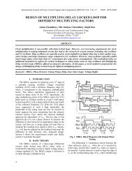
Internati<strong>on</strong>al Journal <strong>of</strong> Power C<strong>on</strong>trol Signal and Computati<strong>on</strong> (IJPCSC) Vol. 2 No. 1 ISSN : 0976-268X<br />
EFFECT ON PERFORMANCE CHARACTERISTICS OF<br />
RECTANGULAR PATCH ANTENNA WITH VARYING HEIGHT OF<br />
DIELECTRIC COVER<br />
1 R.K.Yadav and R.L.Yadava 2<br />
Department <strong>of</strong> Electr<strong>on</strong>ics and Communicati<strong>on</strong> Engineering,<br />
1 I.T.S. Engineering College, Greater Noida, Uttar Pradesh, India<br />
2 Galgotia’s College <strong>of</strong> Engineering and Technology, Uttar Pradesh, India<br />
1 ravipusad@gmail.com, 2 rly1972@gmail.com<br />
ABSTRACT<br />
In this paper, we study the <str<strong>on</strong>g>effect</str<strong>on</strong>g> <strong>on</strong> <strong>performance</strong> <strong>characteristics</strong> <strong>of</strong> <strong>rectangular</strong> <strong>patch</strong> <strong>antenna</strong> with varying<br />
thickness <strong>of</strong> dielectric cover. In this case a coaxial cable fed microstrip line is used which leads to good<br />
impedance matching and its operating frequency is 2.4 to 2.4835 GHz(ISM band). Simulated results are first<br />
used to indicate the design procedures to achieve good impedance matching are discussed. In additi<strong>on</strong>, its<br />
characteristic <str<strong>on</strong>g>effect</str<strong>on</strong>g>s <strong>on</strong> res<strong>on</strong>ant frequency, impedance matching, band width and gain are simulated. And it<br />
has been observed that res<strong>on</strong>ance frequency is shifted toward the lower side <strong>of</strong> frequency <strong>of</strong> operati<strong>on</strong>, while<br />
other parameters have slight variati<strong>on</strong> in their values with the thickness <strong>of</strong> loading.<br />
Keywords - Microstrip Antenna, Dielectric Covers, Frequency Alterati<strong>on</strong>, Envir<strong>on</strong>mental Hazards.<br />
I. INTRODUCTION<br />
Microstrip <strong>antenna</strong>s have several advantages<br />
compared to c<strong>on</strong>venti<strong>on</strong>al microwave <strong>antenna</strong>s;<br />
therefore have many applicati<strong>on</strong>s over broad frequency<br />
range. Microstrip <strong>antenna</strong> is very small radiating<br />
element that can be c<strong>on</strong>structed very precisely due to its<br />
easy c<strong>on</strong>structi<strong>on</strong> method. Its other attractive and<br />
unique properties are; low pr<strong>of</strong>ile, light weight, low<br />
cost, c<strong>on</strong>formable structure and flexibility with regard<br />
to frequency, polarizati<strong>on</strong>, pattern and impedance [1].<br />
Although the sizes <strong>of</strong> microstrip <strong>antenna</strong> with circular<br />
polarizati<strong>on</strong>(CP) radiati<strong>on</strong> are c<strong>on</strong>siderably compact,<br />
they are always marred by problems such as narrow CP<br />
operating bandwidth and high edge impedance that due<br />
to slenderized microstrip. The major drawback <strong>of</strong> the<br />
microstrip <strong>antenna</strong> is its inherent narrow bandwidth,<br />
which is a major obstacle that restricts wider<br />
applicati<strong>on</strong>s. In order to enhance the bandwidth <strong>of</strong><br />
MSA, the numbers <strong>of</strong> techniques have been proposed.<br />
The available literatures, reveal that the envir<strong>on</strong>mental<br />
<str<strong>on</strong>g>effect</str<strong>on</strong>g>s (such as snow, raindrops, etc.) deteriorate the<br />
<strong>performance</strong> <strong>of</strong> <strong>antenna</strong>; particularly res<strong>on</strong>ance<br />
frequency/bandwidth wherever they are used for l<strong>on</strong>g<br />
durati<strong>on</strong>. This is the reas<strong>on</strong>, superstrate (cover)<br />
dielectric layers are <strong>of</strong>ten used to protect microstrip<br />
<strong>antenna</strong> from external hazards, or naturally formed (e.g.<br />
ice layers) during flight or severe weather c<strong>on</strong>diti<strong>on</strong>s.<br />
Whether a cover layer is naturally formed or imposed<br />
by design, it may affect adversely the <strong>antenna</strong><br />
<strong>performance</strong> <strong>characteristics</strong>, such as gain, directivity,<br />
radiati<strong>on</strong> and efficiency. For this reas<strong>on</strong>, it is important<br />
to analyze superstrate loading <str<strong>on</strong>g>effect</str<strong>on</strong>g>s from a<br />
fundamental point <strong>of</strong> view, so that the <strong>performance</strong> may<br />
be understood better or a proper choice <strong>of</strong> cover<br />
parameters may be implemented.<br />
Therefore, several researchers have studied the<br />
<str<strong>on</strong>g>effect</str<strong>on</strong>g> <strong>of</strong> dielectric covers <strong>on</strong> <str<strong>on</strong>g>effect</str<strong>on</strong>g>ive permittivity and<br />
res<strong>on</strong>ant frequency. The res<strong>on</strong>ance and input<br />
impedance <strong>of</strong> covered microstrip <strong>antenna</strong>s using<br />
Spectral domain has been analyzed [2]. While the<br />
variati<strong>on</strong>al technique with transmissi<strong>on</strong> line model was<br />
proposed to calculate the res<strong>on</strong>ant frequency <strong>of</strong> covered<br />
<strong>rectangular</strong> <strong>antenna</strong>. And variati<strong>on</strong>al technique in<br />
Fourier domain to calculate the <strong>rectangular</strong> structure’s<br />
<str<strong>on</strong>g>effect</str<strong>on</strong>g>ive permittivity and res<strong>on</strong>ant <strong>characteristics</strong> <strong>of</strong><br />
<strong>antenna</strong> using Method <strong>of</strong> Moments has been d<strong>on</strong>e by<br />
[3-5]. All <strong>of</strong> these methods are complex and time<br />
c<strong>on</strong>suming and not suitable for direct integrati<strong>on</strong> into<br />
computer aided design (CAD). The cavity model<br />
approach used for a superstrate-loaded circular <strong>patch</strong><br />
[6] is extended and a comprehensive theoretical<br />
formulati<strong>on</strong> is presented. The present analysis does not<br />
involve rigorous mathematical steps or computati<strong>on</strong> as<br />
in [7]. The change in the fringing electric field and<br />
hence the <str<strong>on</strong>g>effect</str<strong>on</strong>g>ive <strong>patch</strong> dimensi<strong>on</strong> caused in the<br />
presence <strong>of</strong> the superstrate is accounted for very<br />
accurately.<br />
Therefore, in this paper, we have observed the<br />
<str<strong>on</strong>g>effect</str<strong>on</strong>g>s <strong>of</strong> dielectric cover <strong>on</strong> the <strong>antenna</strong> <strong>characteristics</strong>.<br />
Theoretical results for the multi-band <strong>performance</strong>,<br />
55
gain, and directivity also are presented. In this paper,<br />
commercial simulator was employed to study the<br />
designs <strong>of</strong> the key parameters for this <strong>rectangular</strong> <strong>patch</strong><br />
microstrip <strong>antenna</strong> fabricated <strong>on</strong> RT-Duroid substrate.<br />
Follow up by c<strong>on</strong>structing and testing several <strong>antenna</strong><br />
prototypes with various side length at a fixed substrate<br />
thickness, details <strong>of</strong> the measured <strong>antenna</strong><br />
<strong>performance</strong>s such as bandwidth, operating centre<br />
frequency and peak gain are presented and discussed. In<br />
additi<strong>on</strong> to the above investigati<strong>on</strong>, superstrate with<br />
various thickness and dielectric c<strong>on</strong>stant loaded <strong>on</strong> the<br />
<strong>rectangular</strong> <strong>patch</strong> microstrip <strong>antenna</strong> are measured.<br />
Although it is well known that the characteristic <str<strong>on</strong>g>effect</str<strong>on</strong>g>s<br />
<strong>of</strong> superstrate loading <strong>on</strong> <strong>patch</strong> <strong>antenna</strong> includes<br />
res<strong>on</strong>ant frequency, resistant and radiating efficiency<br />
reducti<strong>on</strong> etc. [8], these <str<strong>on</strong>g>effect</str<strong>on</strong>g>s can be eliminated by<br />
fine tuning the key parameters <strong>of</strong> the reactangular <strong>patch</strong><br />
microstrip <strong>antenna</strong> introduced.<br />
II. DESIGN OF RECTANGULAR PATCH<br />
ANTENNA<br />
The microstrip <strong>antenna</strong>s have two slots <strong>of</strong> width W<br />
and height h, separated by a transmissi<strong>on</strong> line <strong>of</strong> length<br />
L. The microstrip is essentially a n<strong>on</strong> homogeneous line<br />
<strong>of</strong> two dielectrics, typically the substrate and air.<br />
Hence, most <strong>of</strong> the electric field lines reside in the<br />
substrate and parts <strong>of</strong> some lines in air. As a result, this<br />
transmissi<strong>on</strong> line cannot support pure transverseelectric-magnetic<br />
(TEM) mode <strong>of</strong> transmissi<strong>on</strong>, since<br />
the phase velocities would be different in the air and the<br />
substrate. Instead, the dominant mode <strong>of</strong> propagati<strong>on</strong><br />
would be the quasi-TEM mode. Hence, an <str<strong>on</strong>g>effect</str<strong>on</strong>g>ive<br />
dielectric c<strong>on</strong>stant (ε e ) must be obtained in order to<br />
account for the fringing and the wave propagati<strong>on</strong> in<br />
the line. The value <strong>of</strong> (ε e ) is slightly less then εr<br />
because the fringing fields around the periphery <strong>of</strong> the<br />
<strong>patch</strong> are not c<strong>on</strong>fined in the dielectric substrate but are<br />
also spread in the air. The expressi<strong>on</strong> for (ε e ) is given<br />
by [2]:<br />
Where ε e = Effective dielectric c<strong>on</strong>stant<br />
ε r = Dielectric c<strong>on</strong>stant <strong>of</strong> substrate<br />
h = Height <strong>of</strong> dielectric substrate<br />
W = Width <strong>of</strong> the <strong>patch</strong><br />
C<strong>on</strong>sider Fig 1a below, which shows a <strong>rectangular</strong><br />
microstrip <strong>patch</strong> <strong>antenna</strong> <strong>of</strong> length L, width W resting<br />
<strong>on</strong> a substrate <strong>of</strong> height h. The co-ordinate axis is<br />
selected such that the length is al<strong>on</strong>g the x directi<strong>on</strong>,<br />
width is al<strong>on</strong>g the y directi<strong>on</strong> and the height is al<strong>on</strong>g the<br />
z directi<strong>on</strong>.<br />
Fig 1a. Microstrip Patch Antennas<br />
In order to operate in the fundamental TM 10 mode,<br />
the length <strong>of</strong> the <strong>patch</strong> must be slightly less than λ/2<br />
where λ is the wavelength in the dielectric medium and<br />
is equal to λ o /√(ε e ) where λ o is the free space<br />
wavelength. The TM 10 mode implies that the field<br />
varies <strong>on</strong>e λ/2 cycle al<strong>on</strong>g the length, and there is no<br />
variati<strong>on</strong> al<strong>on</strong>g the width <strong>of</strong> the <strong>patch</strong>. In the Fig 1b<br />
shown below, the microstrip <strong>patch</strong> <strong>antenna</strong> is<br />
represented by two slots, separated by a transmissi<strong>on</strong><br />
line <strong>of</strong> length L and open circuited at both the ends.<br />
Al<strong>on</strong>g the width <strong>of</strong> the <strong>patch</strong>, the voltage is maximum<br />
and current is minimum to the open ends. The fields at<br />
the edges can be resolved into normal and tangential<br />
comp<strong>on</strong>ents with respect to the ground plane.<br />
Fig. 1b Top View <strong>of</strong> Antenna Fig 1c Side View <strong>of</strong><br />
Antenna<br />
It is seen from Fig 1c that the normal comp<strong>on</strong>ents<br />
<strong>of</strong> the electric field at the two edges al<strong>on</strong>g the width are<br />
in opposite directi<strong>on</strong>s and thus out <strong>of</strong> phase since the<br />
<strong>patch</strong> is λ/2 l<strong>on</strong>g and hence they cancel each other in<br />
the broadside directi<strong>on</strong>. The tangential comp<strong>on</strong>ents<br />
(seen in Fig 1c), which are in phase, means that the<br />
resulting fields combine to give maximum radiated<br />
field normal to the surface <strong>of</strong> the structure. Hence the<br />
edges al<strong>on</strong>g the width can be represented as two<br />
radiating slots, which are λ/2 apart and excited in phase<br />
and radiating in the half space above the ground plane.<br />
The fringing fields al<strong>on</strong>g the width can be modeled as<br />
radiating slots and electrically the <strong>patch</strong> <strong>of</strong> the<br />
microstrip <strong>antenna</strong> looks greater than its physical<br />
dimensi<strong>on</strong>s. The dimensi<strong>on</strong>s <strong>of</strong> the <strong>patch</strong> al<strong>on</strong>g its<br />
56
length have now been extended <strong>on</strong> each end by a<br />
distance ΔL, which is given empirically by:<br />
The <str<strong>on</strong>g>effect</str<strong>on</strong>g>ive length <strong>of</strong> the <strong>patch</strong> L eff now becomes;<br />
L eff =L+2ΔL<br />
For a given res<strong>on</strong>ance frequency f 0 ,the <str<strong>on</strong>g>effect</str<strong>on</strong>g>ive length<br />
is given as;<br />
ground plane, thus not making it completely planar for<br />
thick substrates.<br />
III. EFFECT OF DIELECTRIC COVER<br />
In particular, due to dielectric cover the res<strong>on</strong>ance<br />
frequency <strong>of</strong> <strong>antenna</strong> changes, and reas<strong>on</strong> behind that<br />
<str<strong>on</strong>g>effect</str<strong>on</strong>g>ive dielectric c<strong>on</strong>stant changes due to dielectric<br />
layer. And corresp<strong>on</strong>ding fracti<strong>on</strong>al change in<br />
res<strong>on</strong>ance frequency is calculated using [2, 7].<br />
For a <strong>rectangular</strong> microstrip <strong>patch</strong> <strong>antenna</strong>, the<br />
res<strong>on</strong>ance frequency for any TMmn mode is given by;<br />
Where m and n are the modes al<strong>on</strong>g L and W<br />
For efficient radiati<strong>on</strong> the width W is given by [3] as:<br />
Where,<br />
ε e = <str<strong>on</strong>g>effect</str<strong>on</strong>g>ive dielectric c<strong>on</strong>stant with cover<br />
ε eo = <str<strong>on</strong>g>effect</str<strong>on</strong>g>ive dielectric c<strong>on</strong>stant without cover<br />
Δε e = change in dielectric c<strong>on</strong>stant due to cover<br />
Δf r = fracti<strong>on</strong>al change in res<strong>on</strong>ance frequency<br />
f r = Res<strong>on</strong>ance frequency<br />
Fig 2a Structure and design parameters <strong>of</strong> the<br />
<strong>antenna</strong><br />
The geometry and design parameters <strong>of</strong> a<br />
<strong>rectangular</strong> <strong>patch</strong> coaxial cable fed <strong>antenna</strong> are shown<br />
in Fig 2a. A substrate width and length are used as<br />
57.05 mm and 49.05 mm respectively .The dielectric<br />
c<strong>on</strong>stant <strong>of</strong> the substrate used is 2.33.The operating<br />
frequency is in between 2.4 to 2.4835 GHz. Coaxial<br />
feeding is given to the point where input resistance is<br />
50 ohms. The main advantage <strong>of</strong> this type <strong>of</strong> feeding<br />
scheme is that the feed can be placed at any desired<br />
locati<strong>on</strong> inside the <strong>patch</strong> in order to match with its input<br />
impedance. This feed method is easy to fabricate and<br />
has low spurious radiati<strong>on</strong>. However, its major<br />
disadvantage is that it provides narrow bandwidth and<br />
is difficult to model since a hole has to be drilled in the<br />
substrate and the c<strong>on</strong>nector protrudes outside the<br />
Fig 2b. Structure <strong>of</strong> <strong>antenna</strong> with dielectric cover.<br />
The geometry <strong>of</strong> <strong>rectangular</strong> <strong>patch</strong> <strong>antenna</strong> having<br />
dielectric cover is shown in Fig 2b. In reality, the<br />
microstrip <strong>antenna</strong> attached to an electr<strong>on</strong>ic device will<br />
be protected by a dielectric cover (superstrate) that acts<br />
as a shield against hazardous envir<strong>on</strong>mental <str<strong>on</strong>g>effect</str<strong>on</strong>g>s.<br />
These shielding materials, normally plastics (lossy<br />
dielectric), will decrease the overall <strong>performance</strong>s <strong>of</strong><br />
the <strong>antenna</strong> operating <strong>characteristics</strong> such as res<strong>on</strong>ant<br />
frequency, impedance bandwidth and radiating<br />
efficiency [9-10]. In this paper we have used the<br />
dielectric cover <strong>of</strong> various thicknesses and analyze the<br />
<str<strong>on</strong>g>effect</str<strong>on</strong>g>s <strong>of</strong> dielectric cover <strong>on</strong> the different <strong>antenna</strong><br />
parameters.<br />
IV. RESULT AND DISCUSSION<br />
A. Result <strong>of</strong> <strong>rectangular</strong> <strong>patch</strong> <strong>antenna</strong><br />
In order to present the design procedure <strong>of</strong><br />
achieving impedance matching for this case,<br />
dimensi<strong>on</strong>s <strong>of</strong> width and length <strong>of</strong> 57 mm and 49 mm<br />
are selected initially respectively. This dimensi<strong>on</strong> is<br />
calculated corresp<strong>on</strong>ding to 2.3 GHz center frequency.<br />
The first parameter to alter is s and Fig. 3(a) as depicted<br />
57
shown the simulated results <strong>of</strong> the input impedance.<br />
The c<strong>on</strong>stant resistance <strong>of</strong> 50 ohm is taken initially.<br />
Ans<strong>of</strong>t Corporati<strong>on</strong><br />
0.00<br />
-1.00<br />
XY Plot 1<br />
HFSSDesign1<br />
Curve Info<br />
dB(S(WavePort1,WavePort1))<br />
Setup1 : Sw eep1<br />
dB(S(WavePort1,WavePort1))<br />
-2.00<br />
-3.00<br />
-4.00<br />
-5.00<br />
-6.00<br />
1.50 2.00 2.50 3.00<br />
Freq [GHz]<br />
Fig 4(a) Return Loss Vs frequency<br />
Fig 3(a) s-parameter <strong>of</strong> <strong>rectangular</strong> <strong>patch</strong> <strong>antenna</strong><br />
B. Result <strong>of</strong> <strong>rectangular</strong> <strong>patch</strong> <strong>antenna</strong> after optimizati<strong>on</strong><br />
After optimizati<strong>on</strong> it is observed that the results are<br />
better. The s-parameter is shown in Fig 3(b). We got the<br />
center frequency as 2.4GHz and improved <strong>antenna</strong><br />
<strong>characteristics</strong>. Bandwidth after optimizati<strong>on</strong> is<br />
achieved to be 4.34%.The dimensi<strong>on</strong>s <strong>of</strong> length and<br />
width <strong>of</strong> <strong>rectangular</strong> <strong>patch</strong> are same at it is 57.05 mm<br />
and 49.05 mm, at which we get the required center<br />
frequency <strong>of</strong> 2.4 GHz. The return loss is -15 dB, which<br />
is better as compared to that <strong>of</strong> the return loss before<br />
optimizati<strong>on</strong> which was 5.8 dB.<br />
Fig 4(b) Impedance Vs frequency<br />
Fig 3 (b). Return loss <strong>of</strong> the microstrip <strong>antenna</strong><br />
C. Result <strong>of</strong> <strong>rectangular</strong> <strong>patch</strong> <strong>antenna</strong> after dielectric cover<br />
Effects <strong>on</strong> the <strong>antenna</strong> <strong>characteristics</strong> after<br />
applying dielectric cover is shown in Figs 4(a) - 4(d).<br />
The <strong>performance</strong> <strong>characteristics</strong> <strong>of</strong> <strong>antenna</strong> are<br />
decreased after using dielectric cover as shown. The<br />
dimensi<strong>on</strong>s <strong>of</strong> the dielectric cover are 77 mm, 69 mm<br />
and 4mm+2*a. Here ‘a’ is a variable and its value<br />
varies from 0.2 mm to 1mm having step size <strong>of</strong> 0.2 mm.<br />
Here ‘p’ shows the variati<strong>on</strong> in the thickness <strong>of</strong> the<br />
dielectric cover. The variati<strong>on</strong>s in the return loss<br />
<strong>characteristics</strong> and the smith chart are shown below in<br />
the diagrams.<br />
Fig 4(c) Directivity Vs frequency<br />
Fig 4(d) Gain Vs frequency<br />
58
V. CONCLUSION<br />
The key parameters <strong>of</strong> a <strong>rectangular</strong> <strong>patch</strong><br />
microstrip <strong>antenna</strong> are presented and the design<br />
procedures for impedance matching are studied. Several<br />
<strong>antenna</strong> prototypes with various sizes and substrate<br />
thicknesses have been c<strong>on</strong>structed, and the results<br />
revealed that it could reduce the <strong>patch</strong> size for the<br />
<strong>rectangular</strong> <strong>patch</strong> microstrip <strong>antenna</strong> operated at a given<br />
frequency. Based <strong>on</strong> the informati<strong>on</strong> obtained,<br />
superstrate <strong>of</strong> different thickness were loaded <strong>on</strong> the<br />
<strong>rectangular</strong>-<strong>patch</strong> microstrip <strong>antenna</strong> for evaluati<strong>on</strong>.<br />
The results show that the <strong>antenna</strong> <strong>performance</strong>s such as<br />
centre frequency; bandwidth and radiating efficiency<br />
are reduced as expected. IN particular with superstrate<br />
loading <strong>of</strong> thickness 1.0mm and 1.2 mm, the return loss<br />
is found to be -16.29 dB and -16.817 dB at frequencies<br />
2.26 GHz and 2.25 GHz respectively. Therefore, there<br />
is shift <strong>of</strong> 0.01 GHz frequency. The variati<strong>on</strong> <strong>of</strong><br />
impedance with frequency shown in Fig 4 (b) indicates<br />
that there is <str<strong>on</strong>g>effect</str<strong>on</strong>g> <strong>of</strong> dielectric loading <strong>on</strong> impedance<br />
matching <strong>of</strong> the <strong>antenna</strong>. As the thickness <strong>of</strong> superstrate<br />
loading changes the res<strong>on</strong>ance frequency shifted toward<br />
the higher side <strong>of</strong> frequency band. It is also observed<br />
that <strong>antenna</strong> structure exhibits res<strong>on</strong>ances at<br />
frequencies; 2.06 GHz, 2.05 GHz and 1.98 GHz that are<br />
res<strong>on</strong>ance frequency lower as the thickness <strong>of</strong> loading<br />
increases. The variati<strong>on</strong> <strong>of</strong> directivity and gain with<br />
orientati<strong>on</strong> <strong>of</strong> <strong>antenna</strong> shows that there is no much<br />
influence <strong>of</strong> loading <strong>on</strong> these parameters <strong>of</strong> the <strong>antenna</strong>.<br />
Only slight changes are being found with the thickness<br />
<strong>of</strong> the loading.<br />
VI. REFERENCE<br />
[1] R.E. Muns<strong>on</strong>, “C<strong>on</strong>formal Microstrip phased arrays”<br />
,IEEE Trans Antennas propagati<strong>on</strong>, AP-22, pp. 74-78,<br />
Jan 1974.<br />
[2] P.K.Agrawal and M.C. Bailey, “An analysis technique<br />
for feed line microstrip <strong>antenna</strong>s”, IEEE Trans. Antennas<br />
propagati<strong>on</strong>, vol. AP-25, pp. 756-758, Nov. 1977.<br />
[3] I.J.Bahl and S.S. Stuchly, “Analysis <strong>of</strong> Microstrip<br />
covered with a lossy dielectric”, IEEE Trans. Vol. MTT-<br />
28, pp.104- 109, Feb, 1980.<br />
[4] Bahl, I.J., Bhatiya and Stuchly,S.S., “Design <strong>of</strong><br />
microstrip <strong>antenna</strong> covered with a dielectric layer”, IEEE<br />
Trans. AP-30, pp. 314-318, 1982.<br />
[5] H.Pues and A van d Capelle, “Accurate transmissi<strong>on</strong> line<br />
model for the <strong>rectangular</strong> microstrip <strong>antenna</strong>”, IEEE<br />
Proc. Vol. 131,H, pp. 334-340,1984.<br />
[6] Alexopoulos, N.G. and Jacks<strong>on</strong> “Fundamental<br />
superstrate (cover) <str<strong>on</strong>g>effect</str<strong>on</strong>g>s <strong>on</strong> printed circuit <strong>antenna</strong>s”,<br />
IEEE Trans. 1984, AP-32,(S), pp.807-815.<br />
[7] Yadav, R. K & Yadava, R.L, "Superstrate Loaded<br />
Rectangular Microstrip Antennas –An Overview”<br />
Internati<strong>on</strong>al journal <strong>of</strong> Informati<strong>on</strong>, Intelligence and<br />
Knowledge (JIIK) Volume 3, Issue, 2011 (Accepted)<br />
[8] I.J.Bahl, “Build microstrip <strong>antenna</strong> with paper thin<br />
dimensi<strong>on</strong>s”, Microwaves vol.18, pp.50-63, Oct.1979.<br />
[9] R.Shavit , “Dielectric cover <str<strong>on</strong>g>effect</str<strong>on</strong>g> <strong>on</strong> <strong>rectangular</strong><br />
microstrip <strong>antenna</strong> array”, IEEE Trans. Antenna<br />
Propagati<strong>on</strong> AP.42, pp. 1180-1184, 1994.<br />
[10] Yadav R. K. ,Shubham Singh and Jugul Kishore " Effect<br />
<strong>of</strong> Superstrate Loading <strong>on</strong> Rectangular Patch Antenna”<br />
is accepted for the presentati<strong>on</strong> and publicati<strong>on</strong> in<br />
Nati<strong>on</strong>al C<strong>on</strong>ference <strong>on</strong> Trends in signal processing &<br />
Communicati<strong>on</strong> <strong>on</strong> March 10-12, 2011<br />
59