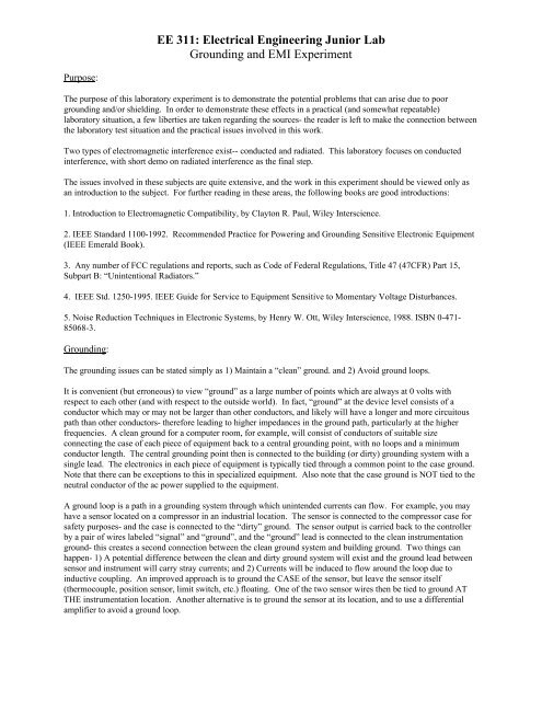
EE 311: Electrical Engineering Junior Lab Grounding and EMI ...
EE 311: Electrical Engineering Junior Lab Grounding and EMI ...
EE 311: Electrical Engineering Junior Lab Grounding and EMI ...

Create successful ePaper yourself
Turn your PDF publications into a flip-book with our unique Google optimized e-Paper software.
<strong>EE</strong> <strong>311</strong>: <strong>Electrical</strong> <strong>Engineering</strong> <strong>Junior</strong> <strong>Lab</strong><br />
<strong>Grounding</strong> <strong>and</strong> <strong>EMI</strong> Experiment<br />
Purpose:<br />
The purpose of this laboratory experiment is to demonstrate the potential problems that can arise due to poor<br />
grounding <strong>and</strong>/or shielding. In order to demonstrate these effects in a practical (<strong>and</strong> somewhat repeatable)<br />
laboratory situation, a few liberties are taken regarding the sources- the reader is left to make the connection between<br />
the laboratory test situation <strong>and</strong> the practical issues involved in this work.<br />
Two types of electromagnetic interference exist-- conducted <strong>and</strong> radiated. This laboratory focuses on conducted<br />
interference, with short demo on radiated interference as the final step.<br />
The issues involved in these subjects are quite extensive, <strong>and</strong> the work in this experiment should be viewed only as<br />
an introduction to the subject. For further reading in these areas, the following books are good introductions:<br />
1. Introduction to Electromagnetic Compatibility, by Clayton R. Paul, Wiley Interscience.<br />
2. I<strong>EE</strong>E St<strong>and</strong>ard 1100-1992. Recommended Practice for Powering <strong>and</strong> <strong>Grounding</strong> Sensitive Electronic Equipment<br />
(I<strong>EE</strong>E Emerald Book).<br />
3. Any number of FCC regulations <strong>and</strong> reports, such as Code of Federal Regulations, Title 47 (47CFR) Part 15,<br />
Subpart B: “Unintentional Radiators.”<br />
4. I<strong>EE</strong>E Std. 1250-1995. I<strong>EE</strong>E Guide for Service to Equipment Sensitive to Momentary Voltage Disturbances.<br />
5. Noise Reduction Techniques in Electronic Systems, by Henry W. Ott, Wiley Interscience, 1988. ISBN 0-471-<br />
85068-3.<br />
<strong>Grounding</strong>:<br />
The grounding issues can be stated simply as 1) Maintain a “clean” ground. <strong>and</strong> 2) Avoid ground loops.<br />
It is convenient (but erroneous) to view “ground” as a large number of points which are always at 0 volts with<br />
respect to each other (<strong>and</strong> with respect to the outside world). In fact, “ground” at the device level consists of a<br />
conductor which may or may not be larger than other conductors, <strong>and</strong> likely will have a longer <strong>and</strong> more circuitous<br />
path than other conductors- therefore leading to higher impedances in the ground path, particularly at the higher<br />
frequencies. A clean ground for a computer room, for example, will consist of conductors of suitable size<br />
connecting the case of each piece of equipment back to a central grounding point, with no loops <strong>and</strong> a minimum<br />
conductor length. The central grounding point then is connected to the building (or dirty) grounding system with a<br />
single lead. The electronics in each piece of equipment is typically tied through a common point to the case ground.<br />
Note that there can be exceptions to this in specialized equipment. Also note that the case ground is NOT tied to the<br />
neutral conductor of the ac power supplied to the equipment.<br />
A ground loop is a path in a grounding system through which unintended currents can flow. For example, you may<br />
have a sensor located on a compressor in an industrial location. The sensor is connected to the compressor case for<br />
safety purposes- <strong>and</strong> the case is connected to the “dirty” ground. The sensor output is carried back to the controller<br />
by a pair of wires labeled “signal” <strong>and</strong> “ground”, <strong>and</strong> the “ground” lead is connected to the clean instrumentation<br />
ground- this creates a second connection between the clean ground system <strong>and</strong> building ground. Two things can<br />
happen- 1) A potential difference between the clean <strong>and</strong> dirty ground system will exist <strong>and</strong> the ground lead between<br />
sensor <strong>and</strong> instrument will carry stray currents; <strong>and</strong> 2) Currents will be induced to flow around the loop due to<br />
inductive coupling. An improved approach is to ground the CASE of the sensor, but leave the sensor itself<br />
(thermocouple, position sensor, limit switch, etc.) floating. One of the two sensor wires then be tied to ground AT<br />
THE instrumentation location. Another alternative is to ground the sensor at its location, <strong>and</strong> to use a differential<br />
amplifier to avoid a ground loop.
The circuit shown below illustrates a common situation: a sensor (thermocouple, strain gauge, etc.) is located some<br />
distance from it's amplifier. There is some ground potential difference due to stray current flow. Connecting the<br />
common point of Vi to ground grid 1 <strong>and</strong> the polarity side of Vi to a simple amplifier would cause amplification of<br />
both the sensor voltage <strong>and</strong> the ground potential difference. Reconnection of the Vi common to ground grid 2 could<br />
remedy this problem- but now the sensor is floating with some potential difference to the local ground voltage, which<br />
can be a safety problem. The third approach we will see is the use of a differential amplifier, which allows Vi to be<br />
tied to local ground but amplifies only Vi <strong>and</strong> not the ground potential difference.<br />
Figure 1. A sensor at one location to be connected to an amplifier at another location.<br />
Figure 2. Proto-board 1 schematic<br />
On your laboratory bench, you are provided with a variety of equipment. Each piece of equipment is tied to the<br />
bench ground wire (the green wire) through the third prong of the plug. In addition, the electronics common point of<br />
some of this equipment is tied to the case, <strong>and</strong> hence to the green wire. In particular, you can count on any st<strong>and</strong>ard<br />
oscilloscope to have the common lead tied to case. Also on this bench, the counter <strong>and</strong> the signal generator are<br />
reference to case. The measurement terminals on digital voltmeters are typically NOT tied to case, <strong>and</strong> this is true<br />
for both DVM’s you will be using in this experiment. You will also be using a signal generator from the instrument
oom that has three terminals - the ground terminal is connected directly to case <strong>and</strong> to the green wire through the<br />
third prong of the plug. To reference the signal to ground, a grounding strap is provided which will tie one side of<br />
the output to ground. A similar situation exists with the portable dc power supply on your bench, which you will use<br />
for a ground source of dc current. The bench power supply, which has a ground terminals tied directly into the green<br />
wire circuit.<br />
In this experiment, connect your electronics to the bench green wire ground through a single point- the black lead on<br />
one of the oscilloscope channels is a reasonable choice.<br />
<strong>Lab</strong> Procedure:<br />
1. On proto-board 1, set up the Hpxxxx oscillator as shown in Figure 2. Verify that the oscillator ground stud is<br />
connected to the third prong of the power plug. The voltage divider is used to provide better control of the<br />
voltage in the milli-volt range that we will be using. The voltage divider will be the only thing located on<br />
the first proto-board that you have been issued. The middle terminal of the oscillator will be the common<br />
point of the voltage divider. In the first set of experiments, the ground strap connecting the ground terminal<br />
<strong>and</strong> the middle terminal will be on. Connect the output of this divider to a pair of studs on the proto-board.<br />
This voltage will be referred to as V i in the following steps.<br />
2. On proto-board 2, set up the op amp as an inverting amplifier with gain of 100. The circuit diagram is shown in<br />
Figure 3. Take some care to make the layout clean <strong>and</strong> neat. Do some quick measurements to make sure<br />
the amplifier is working. At the end of this step, you should have a working amplifier with channels 1 <strong>and</strong> 2<br />
of the oscilloscope connected to V i <strong>and</strong> V o , respectively, <strong>and</strong> DVM's at both locations. There should be a<br />
single ground on each proto-board through the oscillator ground strap on proto-board 1 <strong>and</strong> through either<br />
the scope ground or power supply ground on proto-board 2.<br />
Figure 3. Amplifier schematic—proto-board 2.<br />
3. Connect v i on proto-board 1 to v i on proto-board 2 by a single lead from the respective hot sides. Put the ground<br />
strap in place on the oscillator. Set the oscillator at 1000 hertz. Vary v i from its minimum value to 100<br />
milli-volts, <strong>and</strong> measure the amplifier gain over this range. Plot the results. Also watch the oscilloscope<br />
traces as you do this <strong>and</strong> note anything interesting. (Comment: You are taking a sinusoidal input <strong>and</strong><br />
amplifying it with a linear amplifier- what should the output be like? We are interested in the gain, which<br />
you are measuring with an rms instrument. We are also interested in the wave-shape of the output).<br />
4. Connect the portable dc power supply so that 0.6 amps or so is circulating around the bench ground system. This<br />
simulates a ground loop with this much current flow- a very practical situation. You can complete this<br />
connection by strapping the ground stud on the dc power supply to one of the active terminals of the dc<br />
supply. Connect a lead from the other active terminal to the ground stud of the oscillator. Put the power<br />
supply meter to measure 1.8 amps full scale, <strong>and</strong> adjust the power supply output. Note the effect of the dc<br />
current on the two scope traces- make sure you have the scope set on the dc mode on both channels.<br />
Comment: If you don’t observe anything different, talk to the lab instructor at this point. Repeat the<br />
measurements of Step 3, plot the results, <strong>and</strong> note observations of the scope traces.
5. Turn off the dc ground current. You have been given a special light bulb circuit that takes current from the hot<br />
wire of the plug through the light bulb <strong>and</strong> puts it onto the third prong rather than the normal neutral<br />
connection. Plug this bulb into the far slot on the power strip on the rear of the bench. You are now<br />
injecting about an amp of 60 hertz current into the bench ground system. Repeat the observations <strong>and</strong><br />
measurements of Item 4. Change the oscillator frequency to approximately 60 hertz, <strong>and</strong> observe variations<br />
in waveform with small changes in frequency. What difference do you observe in the "noise"? Comment:<br />
If no effect is noticed, change the location where the light bulb/scope/oscillator are plugged in until you get<br />
a noticeable change. Double check that you have no ground loops in your setup.<br />
6. Put the oscillator back to 1000 hertz, remove the light bulb, <strong>and</strong> put the dc supply back as it was in step 4. An<br />
improvement on the previous results can be made by tying the v i common into the amplifier ground rather<br />
than into the ground on the oscillator. Remove the ground strap from the oscillator, leaving the dc supply<br />
on the oscillator ground stud. Make a connection from v i common on proto-board 1 to the common bus on<br />
proto-board 2. Repeat the measurements of step 4. Note that this step provides a "clean ground" to protoboard<br />
1 by putting in a common connection between proto-boards through which no circulating ground<br />
current can flow. The drawback here is that Vi is not referenced to the local ground- this can create<br />
problems.<br />
7. A better solution yet is to connect the amplifier as a differential amplifier. Rewire the amplifier for the<br />
configuration shown in Figure 4. Replace the ground strap on the oscillator. Repeat the measurements of<br />
step 4.<br />
Figure 4. Differential amplifier schematic.<br />
8. In this type of work, the desired signal voltage is referred to as the differential mode voltage, while the voltage<br />
between one of the oscillator leads <strong>and</strong> amplifier common (as measured by the scope here) is termed the<br />
common mode voltage- common because both signal leads are floating above “ground” by this many volts.<br />
Figure 5 shows an equivalent circuit with the ground loop potential difference shown here as the common<br />
mode voltage above “true ground”. In this experiment, "true ground" is the ground on proto-board 2. The<br />
common mode voltage Vcm is induced in the circuit by either the dc supply or the light bulb. The<br />
differential mode voltage Vdm is the voltage supplied by the oscillator through the voltage divider. Figure<br />
5 shows these voltages with the differential amplifier.<br />
The goodness of an amplifier configuration is often judged by the common mode rejection ratio; see your<br />
circuits book for a definition of this (see pre-lab step 4). Measure the common mode gain <strong>and</strong> the<br />
differential mode gain, <strong>and</strong> determine the common mode rejection ratio for this circuit.<br />
9. Summarize your findings.<br />
10. Electromagnetic interference (<strong>EMI</strong>) takes two forms- conducted <strong>and</strong> radiated. We saw an example of conducted<br />
interference in the previous section. In this section, we will look at radiated electromagnetic interference.<br />
K<strong>EE</strong>P YOUR PREVIOUS SETUP INTACT. You have two leads of about 4-5 feet each carrying a signal
from Vi to the amplifier. (If they are shorter, arrange for leads of this length). These leads may form a loop<br />
with a significant “window” area (if not, rearrange them). You know from previous work that magnetic flux<br />
passing through this window will induce a voltage around this loop. This voltage will be seen as a<br />
differential mode voltage by the amplifier, <strong>and</strong> create errors. Ask the instructor to provide some radiated<br />
interference, <strong>and</strong> observe the resulting wave-shape on the oscilloscope. How can this form of interference<br />
be reduced? Provide specific wiring examples, i.e., wiring type <strong>and</strong> connection topology.<br />
Figure 5. Differential amplifier equivalent circuit showing common mode <strong>and</strong> differential mode voltages.<br />
Pre-lab Assignment:<br />
1. Determine op amp pin assignments for the LM741 op amp, dip package, <strong>and</strong> prepare a layout for proto-board 2.<br />
2. Study the differential amplifier of Figure 4, <strong>and</strong> determine the gain of the amplifier shown.<br />
3. Prepare a PSpice file for Figure 4 circuit <strong>and</strong> verify the gain of step 2. Include verification in the pre-lab report.<br />
4. Find definitions of common mode <strong>and</strong> differential mode voltages, as well as common mode rejection ratio.<br />
Determine a method to experimentally measure the common mode rejection ratio of the differential amplifier. What<br />
is the common mode rejection ratio (CMRR) of an amplifier that amplifies the common mode <strong>and</strong> differential mode<br />
signals with the same ratio?<br />
5. For the circuit illustrated below, what restriction must be placed on the value of R IN in order to keep the ground<br />
noise coupled into the differential amplifier to less then 0.1% of the signal voltage V S ? What is the CMRR of the<br />
circuit expressed in dB for the calculated value of R IN ? Use manufacturer's datasheets to compare the calculated<br />
value of R IN with the input impedance of a general-purpose LM741 series op amp, an AD624 precision<br />
instrumentation amplifier, <strong>and</strong> an AD215 isolation amplifier. State, if any, the general relationship between an<br />
amplifier's CMRR <strong>and</strong> its input impedance?
6. Determine the optimum cabling <strong>and</strong> grounding arrangement for the circuit illustrated below. The circuit consists<br />
of a grounded, low-level low-frequency signal at location A; a differential amplifier at location B; <strong>and</strong> a grounded<br />
load at location C. Do not use any transformers <strong>and</strong> assume that the source at A <strong>and</strong> the load at C must remain<br />
grounded for safety purposes. Describe the benefits of your topology over other possible configurations.<br />
Equipment/Parts List:<br />
Equipment/Parts:<br />
Bench Equipment Used:<br />
1. HP oscillator<br />
2. 2 proto-boards<br />
3. 741 op amp oscilloscope<br />
4. Resistors: 3- 1Kohm <strong>and</strong> bench power supply, +12 volts.<br />
2- 100 kohm, 1- 50ohm<br />
5. Special light bulb variable power supply<br />
6. leads 2 dvm’s<br />
Last revised: 8-25-02/jjc