5-GHz SiGe HBT monolithic radio transceiver with tunable filtering
5-GHz SiGe HBT monolithic radio transceiver with tunable filtering
5-GHz SiGe HBT monolithic radio transceiver with tunable filtering

Create successful ePaper yourself
Turn your PDF publications into a flip-book with our unique Google optimized e-Paper software.
COPELAND et al.: 5-<strong>GHz</strong> <strong>SiGe</strong> <strong>HBT</strong> MONOLITHIC RADIO TRANSCEIVER WITH TUNABLE FILTERING 177<br />
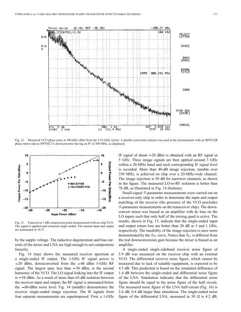
Fig. 12. Measured VCO phase noise at 100-kHz offset from the 3.91-<strong>GHz</strong> carrier. A double-conversion scheme was used in the measurement <strong>with</strong> an HP4352B<br />
phase meter and an HP70427A downconverter having an IF of 300 MHz, as displayed.<br />
Fig. 13. Transceiver 1-dB compression point measurement <strong>with</strong> on-chip VCO.<br />
The signal is applied and extracted single-ended. The unused input and output<br />
are terminated in 50 .<br />
by the supply voltage. The inductive degeneration and bias currents<br />
of the mixer and LNA are high enough to not compromise<br />
linearity.<br />
Fig. 14 (top) shows the measured receiver spectrum at<br />
a single-ended IF output. The 1-<strong>GHz</strong> IF signal power is<br />
20 dBm, downconverted from the 40 dBm 5-<strong>GHz</strong> RF<br />
signal. The largest spur, less than 50 dBm, is the second<br />
harmonic of the VCO. The LO signal leaking into the IF output<br />
is 58 dBm. As a result of more than 65-dB isolation between<br />
the receiver input and output, the RF signal is attenuated below<br />
the 80-dBm noise level. Fig. 14 (middle) demonstrates the<br />
receiver single-ended image rejection. The IF signals from<br />
four separate measurements are superimposed. First, a 1-<strong>GHz</strong><br />
IF signal of about 20 dBm is obtained <strong>with</strong> an RF signal at<br />
5 <strong>GHz</strong>. Three image signals are then applied around 3 <strong>GHz</strong><br />
<strong>with</strong>in a 20-MHz band and each corresponding IF signal level<br />
is recorded. More than 40-dB image rejection, <strong>tunable</strong> over<br />
350 MHz, is achieved on chip over a 20-MHz-wide channel.<br />
The image rejection is 50 dB for narrower channels, as shown<br />
in the figure. The measured LO-to-RF isolation is better than<br />
70 dB, as illustrated in Fig. 14 (bottom).<br />
Small-signal -parameter measurements were carried out on<br />
a receiver-only chip in order to determine the input and output<br />
matching of the receiver (the presence of the VCO precludes<br />
-parameter measurements on the <strong>transceiver</strong> chip). The downconvert<br />
mixer was biased as an amplifier <strong>with</strong> dc bias on the<br />
LO inputs such that only half of the mixing quad is active. The<br />
results, shown in Fig. 15, indicate that the single-ended input<br />
and output return loss are better than 20 dB at 5 and 1 <strong>GHz</strong>,<br />
respectively. The tunability of the image rejection is once more<br />
demonstrated by the curve. Notice that is different from<br />
the real downconversion gain because the mixer is biased as an<br />
amplifier.<br />
A single-ended single-sideband receiver noise figure of<br />
5.9 dB was measured on the receiver chip <strong>with</strong> an external<br />
VCO. The differential receiver noise figure, which cannot be<br />
measured due to lack of suitable equipment, is expected to be<br />
4.5 dB. This prediction is based on the simulated difference of<br />
1.4 dB between the single-ended and differential noise figure<br />
of the LNA. Simulation indicates that the differential noise<br />
figure should be equal to the noise figure of the half circuit.<br />
The measured noise figure of the LNA half-circuit (Fig. 16) is<br />
2.6 dB, 0.4 dB larger than simulation. The single-ended noise<br />
figure of the differential LNA, measured in 50 is 4.2 dB,