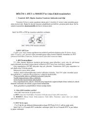
TDA8947J anfi devresi (2x25w 1x50w) - 320Volt
TDA8947J anfi devresi (2x25w 1x50w) - 320Volt
TDA8947J anfi devresi (2x25w 1x50w) - 320Volt

Create successful ePaper yourself
Turn your PDF publications into a flip-book with our unique Google optimized e-Paper software.
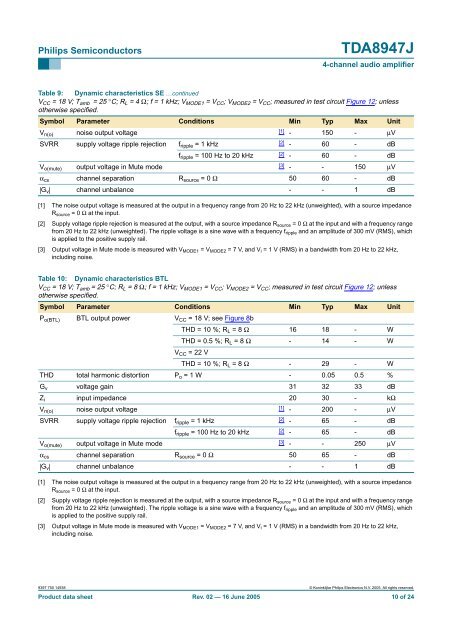
Philips Semiconductors<br />
<strong>TDA8947J</strong><br />
4-channel audio amplifier<br />
Table 9: Dynamic characteristics SE …continued<br />
V CC =18V; T amb =25°C; R L =4Ω; f = 1 kHz; V MODE1 =V CC ; V MODE2 =V CC ; measured in test circuit Figure 12; unless<br />
otherwise specified.<br />
Symbol Parameter Conditions Min Typ Max Unit<br />
V n(o) noise output voltage<br />
[1]<br />
- 150 - µV<br />
SVRR supply voltage ripple rejection f ripple = 1 kHz<br />
[2]<br />
- 60 - dB<br />
f ripple = 100 Hz to 20 kHz<br />
[2]<br />
- 60 - dB<br />
V o(mute) output voltage in Mute mode<br />
[3]<br />
- - 150 µV<br />
α cs channel separation R source =0Ω 50 60 - dB<br />
|G v | channel unbalance - - 1 dB<br />
[1] The noise output voltage is measured at the output in a frequency range from 20 Hz to 22 kHz (unweighted), with a source impedance<br />
R source =0Ω at the input.<br />
[2] Supply voltage ripple rejection is measured at the output, with a source impedance R source =0Ω at the input and with a frequency range<br />
from 20 Hz to 22 kHz (unweighted). The ripple voltage is a sine wave with a frequency f ripple and an amplitude of 300 mV (RMS), which<br />
is applied to the positive supply rail.<br />
[3] Output voltage in Mute mode is measured with V MODE1 =V MODE2 = 7 V, and V i = 1 V (RMS) in a bandwidth from 20 Hz to 22 kHz,<br />
including noise.<br />
Table 10: Dynamic characteristics BTL<br />
V CC =18V; T amb =25°C; R L =8Ω; f = 1 kHz; V MODE1 =V CC ; V MODE2 =V CC ; measured in test circuit Figure 12; unless<br />
otherwise specified.<br />
Symbol Parameter Conditions Min Typ Max Unit<br />
P o(BTL) BTL output power V CC = 18 V; see Figure 8b<br />
THD = 10 %; R L =8Ω 16 18 - W<br />
THD = 0.5 %; R L =8Ω - 14 - W<br />
V CC =22V<br />
THD = 10 %; R L =8Ω - 29 - W<br />
THD total harmonic distortion P o = 1 W - 0.05 0.5 %<br />
G v voltage gain 31 32 33 dB<br />
Z i input impedance 20 30 - kΩ<br />
V n(o) noise output voltage<br />
[1]<br />
- 200 - µV<br />
SVRR supply voltage ripple rejection f ripple = 1 kHz<br />
[2]<br />
- 65 - dB<br />
f ripple = 100 Hz to 20 kHz<br />
[2]<br />
- 65 - dB<br />
V o(mute) output voltage in Mute mode<br />
[3]<br />
- - 250 µV<br />
α cs channel separation R source =0Ω 50 65 - dB<br />
|G v | channel unbalance - - 1 dB<br />
[1] The noise output voltage is measured at the output in a frequency range from 20 Hz to 22 kHz (unweighted), with a source impedance<br />
R source =0Ω at the input.<br />
[2] Supply voltage ripple rejection is measured at the output, with a source impedance R source =0Ω at the input and with a frequency range<br />
from 20 Hz to 22 kHz (unweighted). The ripple voltage is a sine wave with a frequency f ripple and an amplitude of 300 mV (RMS), which<br />
is applied to the positive supply rail.<br />
[3] Output voltage in Mute mode is measured with V MODE1 =V MODE2 = 7 V, and V i = 1 V (RMS) in a bandwidth from 20 Hz to 22 kHz,<br />
including noise.<br />
9397 750 14938 © Koninklijke Philips Electronics N.V. 2005. All rights reserved.<br />
Product data sheet Rev. 02 — 16 June 2005 10 of 24