TDA8947J anfi devresi (2x25w 1x50w) - 320Volt
TDA8947J anfi devresi (2x25w 1x50w) - 320Volt
TDA8947J anfi devresi (2x25w 1x50w) - 320Volt

You also want an ePaper? Increase the reach of your titles
YUMPU automatically turns print PDFs into web optimized ePapers that Google loves.
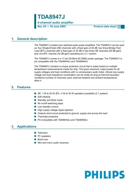
<strong>TDA8947J</strong><br />
4-channel audio amplifier<br />
Rev. 02 — 16 June 2005<br />
Product data sheet<br />
1. General description<br />
2. Features<br />
3. Applications<br />
The <strong>TDA8947J</strong> contains four identical audio power amplifiers. The <strong>TDA8947J</strong> can be used<br />
as: four Single-Ended (SE) channels with a fixed gain of 26 dB, two times Bridge-Tied<br />
Load (BTL) channels with a fixed gain of 32 dB or two times SE channels (26 dB gain)<br />
plus one BTL channel (32 dB gain) operating as a 2.1 system<br />
The <strong>TDA8947J</strong> comes in a 17-pin Dil-Bent-Sil (DBS) power package. The <strong>TDA8947J</strong> is<br />
pin compatible with the TDA8944AJ and TDA8946AJ.<br />
The <strong>TDA8947J</strong> contains a unique protection circuit that is solely based on multiple<br />
temperature measurements inside the chip. This gives maximum output power for all<br />
supply voltages and load conditions with no unnecessary audio holes. Almost any supply<br />
voltage and load impedance combination can be made as long as thermal boundary<br />
conditions (number of channels used, external heatsink and ambient temperature)<br />
allow it.<br />
■ SE: 1 W to 25 W, BTL: 4 W to 50 W operation possibility (2.1 system)<br />
■ Soft clipping<br />
■ Standby and Mute mode<br />
■ No on/off switching plops<br />
■ Low standby current<br />
■ High supply voltage ripple rejection<br />
■ Outputs short-circuit protected to ground, supply and across the load<br />
■ Thermally protected<br />
■ Pin compatible with TDA8944AJ and TDA8946AJ<br />
■ Television<br />
■ PC speakers<br />
■ Boom box<br />
■ Mini and micro audio receivers
Philips Semiconductors<br />
<strong>TDA8947J</strong><br />
4-channel audio amplifier<br />
4. Quick reference data<br />
5. Ordering information<br />
Table 1: Quick reference data<br />
Symbol Parameter Conditions Min Typ Max Unit<br />
V CC supply voltage operating 9 18 26 V<br />
no (clipping) signal<br />
[1]<br />
- - 28 V<br />
I q quiescent supply current V CC =18V; R L = ∞ - 100 145 mA<br />
I stb standby supply current - - 10 µA<br />
P o(SE) SE output power THD = 10 %; R L =4Ω<br />
V CC =18V 7 8.5 - W<br />
V CC =22V - 14 - W<br />
P o(BTL) BTL output power THD = 10 %; R L =8Ω<br />
V CC =18V 16 18 - W<br />
V CC =22V - 29 - W<br />
THD total harmonic distortion SE; P o = 1 W - 0.1 0.5 %<br />
BTL; P o = 1 W - 0.05 0.5 %<br />
G v(max) maximum voltage gain SE 25 26 27 dB<br />
BTL 31 32 33 dB<br />
SVRR supply voltage ripple SE; f = 1 kHz - 60 - dB<br />
rejection<br />
BTL; f = 1 kHz - 65 - dB<br />
[1] The amplifier can deliver output power with non clipping output signals into nominal loads as long as the<br />
ratings of the IC are not exceeded.<br />
Table 2: Ordering information<br />
Type number Package<br />
Name Description Version<br />
<strong>TDA8947J</strong> DBS17P plastic DIL-bent-SIL power package; 17 leads<br />
(lead length 12 mm)<br />
SOT243-1<br />
9397 750 14938 © Koninklijke Philips Electronics N.V. 2005. All rights reserved.<br />
Product data sheet Rev. 02 — 16 June 2005 2 of 24
Philips Semiconductors<br />
<strong>TDA8947J</strong><br />
4-channel audio amplifier<br />
6. Block diagram<br />
V CC1<br />
V CC2<br />
3<br />
16<br />
IN1+<br />
8<br />
1<br />
OUT1+<br />
60 kΩ<br />
IN2+<br />
6<br />
4<br />
OUT2−<br />
60 kΩ<br />
IN3+<br />
9<br />
14<br />
OUT3−<br />
60 kΩ<br />
IN4+<br />
12<br />
17<br />
OUT4+<br />
60 kΩ<br />
CIV<br />
13<br />
V CC<br />
SHORT-CIRCUIT<br />
AND<br />
TEMPERATURE<br />
PROTECTION<br />
SVR<br />
11<br />
0.5V CC<br />
SGND<br />
7<br />
V ref<br />
MODE1<br />
MODE2<br />
10<br />
5<br />
STANDBY ALL<br />
MUTE ALL<br />
ON 1 + 2<br />
MUTE 3 + 4<br />
ON 3 + 4<br />
<strong>TDA8947J</strong><br />
2 15<br />
mdb014<br />
GND1<br />
GND2<br />
Fig 1.<br />
Block diagram<br />
9397 750 14938 © Koninklijke Philips Electronics N.V. 2005. All rights reserved.<br />
Product data sheet Rev. 02 — 16 June 2005 3 of 24
Philips Semiconductors<br />
<strong>TDA8947J</strong><br />
4-channel audio amplifier<br />
7. Pinning information<br />
7.1 Pinning<br />
OUT1+<br />
GND1<br />
V CC1<br />
OUT2−<br />
MODE2<br />
IN2+<br />
SGND<br />
IN1+<br />
IN3+<br />
MODE1<br />
SVR<br />
IN4+<br />
CIV<br />
OUT3−<br />
GND2<br />
V CC2<br />
OUT4+<br />
1<br />
2<br />
3<br />
4<br />
5<br />
6<br />
7<br />
8<br />
9<br />
10<br />
11<br />
12<br />
13<br />
14<br />
15<br />
16<br />
17<br />
<strong>TDA8947J</strong><br />
001aac740<br />
Fig 2.<br />
Pin configuration<br />
7.2 Pin description<br />
Table 3:<br />
Pin description<br />
Symbol Pin Description<br />
OUT1+ 1 non inverted loudspeaker output of channel 1<br />
GND1 2 ground of channels 1 and 2<br />
V CC1 3 supply voltage channels 1 and 2<br />
OUT2− 4 inverted loudspeaker output of channel 2<br />
MODE2 5 mode selection 2 input: Mute and On mode for channels 3 and 4<br />
IN2+ 6 input channel 2<br />
SGND 7 signal ground<br />
IN1+ 8 input channel 1<br />
IN3+ 9 input channel 3<br />
MODE1 10 mode selection 1 input: Standby, Mute and On mode for all<br />
channels<br />
SVR 11 half supply voltage decoupling (ripple rejection)<br />
IN4+ 12 input channel 4<br />
CIV 13 common input voltage decoupling<br />
OUT3− 14 inverted loudspeaker output of channel 3<br />
GND2 15 ground of channels 3 and 4<br />
9397 750 14938 © Koninklijke Philips Electronics N.V. 2005. All rights reserved.<br />
Product data sheet Rev. 02 — 16 June 2005 4 of 24
Philips Semiconductors<br />
<strong>TDA8947J</strong><br />
4-channel audio amplifier<br />
8. Functional description<br />
Table 3: Pin description …continued<br />
Symbol Pin Description<br />
V CC2 16 supply voltage channels 3 and 4<br />
OUT4+ 17 non inverted loudspeaker output of channel 4<br />
TAB - back side tab or heat spreader has to be connected to ground<br />
8.1 Input configuration<br />
The input cut-off frequency is:<br />
1<br />
f i( cut – off )<br />
=<br />
----------------------------<br />
2π( R i × C i )<br />
(1)<br />
For SE application R i = 60 kΩ and C i = 220 nF:<br />
1<br />
f i( cut – off )<br />
= ----------------------------------------------------------------<br />
2π( 60 × 10 3 × 220 × 10 – 9 = 12 Hz<br />
)<br />
(2)<br />
For BTL application R i = 30 kΩ and C i = 470 nF:<br />
1<br />
f i( cut – off )<br />
= ----------------------------------------------------------------<br />
2π( 30 × 10 3 × 470 × 10 – 9 = 11 Hz<br />
)<br />
(3)<br />
As shown in Equation 2 and Equation 3, large capacitor values for the inputs are not<br />
necessary, so the switch-on delay during charging of the input capacitors can be<br />
minimized. This results in a good low frequency response and good switch-on behavior.<br />
8.2 Power amplifier<br />
The power amplifier is a BTL and/or SE amplifier with an all-NPN output stage, capable of<br />
delivering a peak output current of 4 A.<br />
Using the <strong>TDA8947J</strong> as a BTL amplifier offers the following advantages:<br />
• Low peak value of the supply current<br />
• Ripple frequency on the supply voltage is twice the signal frequency<br />
• No expensive DC-blocking capacitor<br />
• Good low frequency performance<br />
9397 750 14938 © Koninklijke Philips Electronics N.V. 2005. All rights reserved.<br />
Product data sheet Rev. 02 — 16 June 2005 5 of 24
Philips Semiconductors<br />
<strong>TDA8947J</strong><br />
4-channel audio amplifier<br />
8.2.1 Output power measurement<br />
The output power as a function of the supply voltage is measured on the output pins at<br />
THD = 10 %; see Figure 8.<br />
The maximum output power is limited by the supply voltage (V CC = 26 V) and the<br />
maximum output current (I o = 4 A repetitive peak current).<br />
For supply voltages V CC > 22 V, a minimum load is required; see Figure 5:<br />
• SE: R L =3Ω<br />
• BTL: R L =6Ω<br />
8.2.2 Headroom<br />
Typical CD music requires at least 12 dB (factor 15.85) dynamic headroom, compared to<br />
the average power output, for transferring the loudest parts without distortion.<br />
The Average Listening Level (ALL) music power, without any distortion, yields:<br />
• SE at P o(SE) =5W, V CC =18V, R L =4Ω and THD = 0.2 %:<br />
5 ⋅ 10 3<br />
( )SE = --------------- = 315 mW<br />
15.85<br />
P o ALL<br />
(4)<br />
• BTL at P o(BTL) =10W, V CC =18V, R L =8Ω and THD = 0.1 %:<br />
10 ⋅ 10 3<br />
( )BTL = ------------------ = 630 mW<br />
15.85<br />
P o ALL<br />
(5)<br />
The power dissipation can be derived from Figure 9 (SE and BTL) for a headroom of 0 dB<br />
and 12 dB, respectively.<br />
Table 4:<br />
For heatsink calculation at the average listening level, a power dissipation of 9 W can be<br />
used.<br />
8.3 Mode selection<br />
Power rating as function of headroom<br />
Headroom Power output Power dissipation (all<br />
SE<br />
BTL<br />
channels driven)<br />
0dB P o =5W P o =10W P D =17W<br />
12 dB P o(ALL) = 315 mW P o(ALL) = 630 mW P D =9W<br />
The <strong>TDA8947J</strong> has three functional modes which can be selected by applying the proper<br />
DC voltage to pin MODE1.<br />
Standby — The current consumption is very low and the outputs are floating. The device<br />
is in the Standby mode when V MODE1 < 0.8 V, or when the MODE1 pin is grounded. In the<br />
Standby mode, the function of pin MODE2 has been disabled.<br />
Mute — The amplifier is DC-biased, but not operational (no audio output). This allows the<br />
input coupling capacitors to be charged to avoid pop-noise. The device is in the Mute<br />
mode when 4.5 V
Philips Semiconductors<br />
<strong>TDA8947J</strong><br />
4-channel audio amplifier<br />
On — The amplifier is operating normally. The On mode is activated at<br />
V MODE1 >(V CC − 2.0 V). The output of channels 3 and 4 can be set to Mute or On mode.<br />
The output channels 3 and 4 can be switched on/off by applying a proper DC voltage to<br />
pin MODE2, under the condition that the output channels 1 and 2 are in the On mode (see<br />
Figure 3).<br />
Table 5: Mode selection<br />
Voltage on pin Channel 1 and 2 Channel 3 and 4<br />
MODE1<br />
MODE2<br />
(sub woofer)<br />
0 V to 0.8 V 0 V to V CC Standby mode Standby mode<br />
4.5 V to (V CC − 3.5 V) 0 V to V CC Mute mode Mute mode<br />
(V CC − 2.0 V) to V CC 0 V to (V CC − 3.5 V) On mode Mute mode<br />
(V CC − 2 V) to V CC On mode On mode<br />
all standby<br />
all mute<br />
channels 1 + 2: on<br />
channels 3 + 4: on or mute<br />
0.8 4.5 V CC −3.5 V CC −2.0 V CC<br />
V MODE1<br />
channels 3 + 4: mute<br />
channels 3 + 4: on<br />
mdb016<br />
V CC −3.5<br />
V CC −2.0<br />
V CC<br />
V MODE2<br />
Fig 3.<br />
Mode selection<br />
8.4 Supply voltage ripple rejection<br />
The Supply Voltage Ripple Rejection (SVRR) is measured with an electrolytic capacitor of<br />
150 µF on pin SVR using a bandwidth of 20 Hz to 22 kHz. Figure 11 illustrates the SVRR<br />
as function of the frequency. A larger capacitor value on pin SVR improves the ripple<br />
rejection behavior at the lower frequencies.<br />
9397 750 14938 © Koninklijke Philips Electronics N.V. 2005. All rights reserved.<br />
Product data sheet Rev. 02 — 16 June 2005 7 of 24
Philips Semiconductors<br />
<strong>TDA8947J</strong><br />
4-channel audio amplifier<br />
9. Limiting values<br />
8.5 Built-in protection circuits<br />
The <strong>TDA8947J</strong> contains two types of detection sensors: one measures local temperatures<br />
of the power stages and one measures the global chip temperature. At a local<br />
temperature of approximately 185 °C or a global temperature of approximately 150 °C,<br />
this detection circuit switches off the power stages for 2 ms. High-impedance of the<br />
outputs is the result. After this time period the power stages switch on automatically and<br />
the detection will take place again; still a too high temperature switches off the power<br />
stages immediately. This protects the <strong>TDA8947J</strong> against shorts to ground, to the supply<br />
voltage and across the load, and against too high chip temperatures.<br />
The protection will only be activated when necessary, so even during a short-circuit<br />
condition, a certain amount of (pulsed) current will still be flowing through the short, just as<br />
much as the power stage can handle without exceeding the critical temperature level.<br />
10. Thermal characteristics<br />
Table 6: Limiting values<br />
In accordance with the Absolute Maximum Rating System (IEC 60134).<br />
Symbol Parameter Conditions Min Max Unit<br />
V CC supply voltage operating −0.3 +26 V<br />
no (clipping) signal<br />
[1]<br />
−0.3 +28 V<br />
V I input voltage −0.3 V CC + 0.3 V<br />
I ORM repetitive peak output<br />
- 4 A<br />
current<br />
T stg storage temperature non-operating −55 +150 °C<br />
T amb ambient temperature −40 +85 °C<br />
P tot total power dissipation - 69 W<br />
V CC(sc) supply voltage to guarantee<br />
short-circuit protection<br />
- 24 V<br />
[1] The amplifier can deliver output power with non clipping output signals into nominal loads as long as the<br />
ratings of the IC are not exceeded.<br />
Table 7: Thermal characteristics<br />
Symbol Parameter Conditions Typ Unit<br />
R th(j-a) thermal resistance from junction to ambient in free air 40 K/W<br />
R th(j-c) thermal resistance from junction to case all channels driven 1.3 K/W<br />
9397 750 14938 © Koninklijke Philips Electronics N.V. 2005. All rights reserved.<br />
Product data sheet Rev. 02 — 16 June 2005 8 of 24
Philips Semiconductors<br />
<strong>TDA8947J</strong><br />
4-channel audio amplifier<br />
11. Static characteristics<br />
Table 8: Static characteristics<br />
V CC =18V; T amb =25°C; R L =8Ω; V MODE1 =V CC ; V MODE2 =V CC ; V i = 0 V; measured in test circuit Figure 12; unless<br />
otherwise specified.<br />
Symbol Parameter Conditions Min Typ Max Unit<br />
Supply<br />
V CC supply voltage operating<br />
[1]<br />
9 18 26 V<br />
no (clipping) signal<br />
[2]<br />
- - 28 V<br />
I q quiescent supply current R L = ∞<br />
[3]<br />
- 100 145 mA<br />
I stb standby supply current - - 10 µA<br />
Output pins<br />
V O DC output voltage<br />
[4]<br />
- 9 - V<br />
∆V OUT differential output voltage offset BTL mode<br />
[5]<br />
- - 170 mV<br />
Mode selection pins<br />
V MODE1 selection voltage on pin On mode V CC − 2.0 - V CC V<br />
MODE1<br />
Mute mode 4.5 - V CC − 3.5 V<br />
Standby mode 0 - 0.8 V<br />
V MODE2 selection voltage on pin On mode: channels 3 and 4<br />
[6]<br />
V CC − 2.0 - V CC V<br />
MODE2<br />
Mute mode: channels 3 and 4 0 - V CC − 3.5 V<br />
I MODE1 selection current on pin MODE1 0 V < V MODE1 < (V CC − 3.5 V) - - 20 µA<br />
I MODE2 selection current on pin MODE2 0 V < V MODE2 < (V CC − 3.5 V) - - 20 µA<br />
[1] A minimum load is required at supply voltages of V CC >22V: R L =3Ω for SE and R L =6Ω for BTL.<br />
[2] The amplifier can deliver output power with non clipping output signals into nominal loads as long as the ratings of the IC are not<br />
exceeded.<br />
[3] With a load connected at the outputs the quiescent current will increase.<br />
[4] The DC output voltage, with respect to ground, is approximately 0.5V CC .<br />
[5] ∆V OUT = |V OUT+ − V OUT- |<br />
[6] Channels 3 and 4 can only be set to Mute or On mode by MODE2 when V MODE1 >V CC − 2.0 V.<br />
12. Dynamic characteristics<br />
Table 9: Dynamic characteristics SE<br />
V CC =18V; T amb =25°C; R L =4Ω; f = 1 kHz; V MODE1 =V CC ; V MODE2 =V CC ; measured in test circuit Figure 12; unless<br />
otherwise specified.<br />
Symbol Parameter Conditions Min Typ Max Unit<br />
P o(SE) SE output power V CC = 18 V; see Figure 8a<br />
THD = 10 %; R L =4Ω 7 8.5 - W<br />
THD = 0.5 %; R L =4Ω - 6.5 - W<br />
V CC =22V<br />
THD = 10 %; R L =4Ω - 14 - W<br />
THD total harmonic distortion P o = 1 W - 0.1 0.5 %<br />
G v voltage gain 25 26 27 dB<br />
Z i input impedance 40 60 - kΩ<br />
9397 750 14938 © Koninklijke Philips Electronics N.V. 2005. All rights reserved.<br />
Product data sheet Rev. 02 — 16 June 2005 9 of 24
Philips Semiconductors<br />
<strong>TDA8947J</strong><br />
4-channel audio amplifier<br />
Table 9: Dynamic characteristics SE …continued<br />
V CC =18V; T amb =25°C; R L =4Ω; f = 1 kHz; V MODE1 =V CC ; V MODE2 =V CC ; measured in test circuit Figure 12; unless<br />
otherwise specified.<br />
Symbol Parameter Conditions Min Typ Max Unit<br />
V n(o) noise output voltage<br />
[1]<br />
- 150 - µV<br />
SVRR supply voltage ripple rejection f ripple = 1 kHz<br />
[2]<br />
- 60 - dB<br />
f ripple = 100 Hz to 20 kHz<br />
[2]<br />
- 60 - dB<br />
V o(mute) output voltage in Mute mode<br />
[3]<br />
- - 150 µV<br />
α cs channel separation R source =0Ω 50 60 - dB<br />
|G v | channel unbalance - - 1 dB<br />
[1] The noise output voltage is measured at the output in a frequency range from 20 Hz to 22 kHz (unweighted), with a source impedance<br />
R source =0Ω at the input.<br />
[2] Supply voltage ripple rejection is measured at the output, with a source impedance R source =0Ω at the input and with a frequency range<br />
from 20 Hz to 22 kHz (unweighted). The ripple voltage is a sine wave with a frequency f ripple and an amplitude of 300 mV (RMS), which<br />
is applied to the positive supply rail.<br />
[3] Output voltage in Mute mode is measured with V MODE1 =V MODE2 = 7 V, and V i = 1 V (RMS) in a bandwidth from 20 Hz to 22 kHz,<br />
including noise.<br />
Table 10: Dynamic characteristics BTL<br />
V CC =18V; T amb =25°C; R L =8Ω; f = 1 kHz; V MODE1 =V CC ; V MODE2 =V CC ; measured in test circuit Figure 12; unless<br />
otherwise specified.<br />
Symbol Parameter Conditions Min Typ Max Unit<br />
P o(BTL) BTL output power V CC = 18 V; see Figure 8b<br />
THD = 10 %; R L =8Ω 16 18 - W<br />
THD = 0.5 %; R L =8Ω - 14 - W<br />
V CC =22V<br />
THD = 10 %; R L =8Ω - 29 - W<br />
THD total harmonic distortion P o = 1 W - 0.05 0.5 %<br />
G v voltage gain 31 32 33 dB<br />
Z i input impedance 20 30 - kΩ<br />
V n(o) noise output voltage<br />
[1]<br />
- 200 - µV<br />
SVRR supply voltage ripple rejection f ripple = 1 kHz<br />
[2]<br />
- 65 - dB<br />
f ripple = 100 Hz to 20 kHz<br />
[2]<br />
- 65 - dB<br />
V o(mute) output voltage in Mute mode<br />
[3]<br />
- - 250 µV<br />
α cs channel separation R source =0Ω 50 65 - dB<br />
|G v | channel unbalance - - 1 dB<br />
[1] The noise output voltage is measured at the output in a frequency range from 20 Hz to 22 kHz (unweighted), with a source impedance<br />
R source =0Ω at the input.<br />
[2] Supply voltage ripple rejection is measured at the output, with a source impedance R source =0Ω at the input and with a frequency range<br />
from 20 Hz to 22 kHz (unweighted). The ripple voltage is a sine wave with a frequency f ripple and an amplitude of 300 mV (RMS), which<br />
is applied to the positive supply rail.<br />
[3] Output voltage in Mute mode is measured with V MODE1 =V MODE2 = 7 V, and V i = 1 V (RMS) in a bandwidth from 20 Hz to 22 kHz,<br />
including noise.<br />
9397 750 14938 © Koninklijke Philips Electronics N.V. 2005. All rights reserved.<br />
Product data sheet Rev. 02 — 16 June 2005 10 of 24
Philips Semiconductors<br />
<strong>TDA8947J</strong><br />
4-channel audio amplifier<br />
10 7<br />
V o<br />
(µV)<br />
10 6<br />
coc005<br />
10 5<br />
10 4<br />
10 3<br />
10 2<br />
10<br />
1<br />
0 4 8 12<br />
16 20<br />
V MODE1 (V)<br />
Fig 4.<br />
BTL; V CC =18V; V i =50mV.<br />
AC output voltage as function of voltage on pin MODE1<br />
60<br />
mce485<br />
60<br />
mce484<br />
P o<br />
(W)<br />
P o<br />
(W)<br />
4 Ω<br />
6 Ω<br />
40<br />
40<br />
8 Ω<br />
2 Ω<br />
3 Ω<br />
20<br />
20<br />
R L = 2 Ω<br />
16 Ω<br />
R L = 1 Ω<br />
4 Ω<br />
8 Ω<br />
0<br />
8<br />
12 16 20 24 28<br />
V CC (V)<br />
0<br />
8<br />
12 16 20 24 28<br />
V CC (V)<br />
THD = 10 %; one channel.<br />
THD = 10 %; one channel.<br />
a. SE b. BTL<br />
Fig 5. Output power as function of supply voltage at various loads<br />
9397 750 14938 © Koninklijke Philips Electronics N.V. 2005. All rights reserved.<br />
Product data sheet Rev. 02 — 16 June 2005 11 of 24
Philips Semiconductors<br />
<strong>TDA8947J</strong><br />
4-channel audio amplifier<br />
10 2<br />
mce488<br />
THD + N<br />
(%)<br />
10<br />
1<br />
10 −1<br />
10 −2<br />
10 −1 1 10<br />
10 2<br />
P o (W)<br />
mce487<br />
10 2<br />
10 −2<br />
THD + N<br />
(%)<br />
10<br />
1<br />
10 −1<br />
10 −1 1<br />
10<br />
P o (W)<br />
10 2<br />
V CC = 18 V; f = 1 kHz; R L =4Ω.<br />
V CC = 18 V; f = 1 kHz; R L =8Ω.<br />
a. SE b. BTL<br />
Fig 6. Total harmonic distortion-plus-noise as function of output power<br />
10<br />
mce489<br />
10<br />
mce490<br />
10<br />
10<br />
10 2 10 3 10 4 f (Hz)<br />
10 5 10 10 2 10 3 10 4 f (Hz)<br />
10 5<br />
THD + N<br />
THD + N<br />
(%)<br />
(%)<br />
1<br />
10 −1<br />
1<br />
10 −1<br />
V CC = 18 V; P o = 1 W; R L =4Ω.<br />
V CC = 18 V; P o = 1 W; R L =8Ω.<br />
a. SE b. BTL<br />
Fig 7. Total harmonic distortion-plus-noise as function of frequency<br />
9397 750 14938 © Koninklijke Philips Electronics N.V. 2005. All rights reserved.<br />
Product data sheet Rev. 02 — 16 June 2005 12 of 24
Philips Semiconductors<br />
<strong>TDA8947J</strong><br />
4-channel audio amplifier<br />
50<br />
mce491<br />
50<br />
mce492<br />
P o<br />
(W)<br />
40<br />
P o<br />
(W)<br />
40<br />
30<br />
30<br />
20<br />
20<br />
10<br />
10<br />
0<br />
8 12 16 20 24 28<br />
V CC (V)<br />
0<br />
8 12 16 20 24 28<br />
V CC (V)<br />
THD = 10 %; R L =4Ω; f = 1 kHz.<br />
THD = 10 %; R L =8Ω; f = 1 kHz.<br />
a. SE b. BTL<br />
Fig 8. Output power as function of supply voltage<br />
20<br />
mce493<br />
20<br />
mce494<br />
P D<br />
(W)<br />
16<br />
P D<br />
(W)<br />
16<br />
12<br />
12<br />
8<br />
8<br />
4<br />
4<br />
0<br />
0<br />
0 4 8 12 16 20<br />
0 4 8 12 16 20<br />
P o (W)<br />
P o (W)<br />
V CC = 18 V; R L =4Ω.<br />
V CC = 18 V; R L =8Ω.<br />
a. SE b. BTL<br />
Fig 9. Total power dissipation as function of channel output power per channel (worst case, all channels driven)<br />
9397 750 14938 © Koninklijke Philips Electronics N.V. 2005. All rights reserved.<br />
Product data sheet Rev. 02 — 16 June 2005 13 of 24
Philips Semiconductors<br />
<strong>TDA8947J</strong><br />
4-channel audio amplifier<br />
0<br />
mce495<br />
0<br />
mce496<br />
α cs<br />
(dB)<br />
α cs<br />
(dB)<br />
−20<br />
−20<br />
−40<br />
−40<br />
−60<br />
−60<br />
−80<br />
−80<br />
−100<br />
10<br />
10 2 10 3 10 4 10 5 −100<br />
10<br />
f (Hz)<br />
10 2 10 3 10 4 10 5<br />
f (Hz)<br />
V CC = 18 V; R L =4Ω.<br />
V CC = 18 V; R L =8Ω.<br />
a. SE b. BTL<br />
Fig 10. Channel separation as function of frequency (no bandpass filter applied)<br />
0<br />
mce497<br />
0<br />
mce498<br />
SVRR<br />
(dB)<br />
SVRR<br />
(dB)<br />
−20<br />
−20<br />
−40<br />
−40<br />
−60<br />
−60<br />
−80<br />
10<br />
−80<br />
10 2 10 3 10 4 10 5 10<br />
f (Hz)<br />
10 2 10 3 10 4 10 5<br />
f (Hz)<br />
V CC = 18 V; R source =0Ω; V ripple = 300 mV (RMS).<br />
A bandpass filter of 20 Hz to 22 kHz has been<br />
applied.<br />
Inputs short-circuited.<br />
V CC = 18 V; R source =0Ω; V ripple = 300 mV (RMS).<br />
A bandpass filter of 20 Hz to 22 kHz has been<br />
applied.<br />
Inputs short-circuited.<br />
a. SE b. BTL<br />
Fig 11. Supply voltage ripple rejection as function of frequency<br />
9397 750 14938 © Koninklijke Philips Electronics N.V. 2005. All rights reserved.<br />
Product data sheet Rev. 02 — 16 June 2005 14 of 24
Philips Semiconductors<br />
<strong>TDA8947J</strong><br />
4-channel audio amplifier<br />
13. Application information<br />
13.1 Application diagrams<br />
V CC<br />
V CC1<br />
V CC2<br />
100 nF<br />
1000 µF<br />
3<br />
16<br />
220 nF IN1+ 8<br />
1 OUT1+<br />
V i<br />
V i<br />
220 nF<br />
IN2+<br />
6<br />
60 kΩ<br />
60 kΩ<br />
4<br />
OUT2−<br />
−<br />
+<br />
R L<br />
4 Ω<br />
+<br />
−<br />
R L<br />
4 Ω<br />
10<br />
kΩ<br />
50<br />
kΩ<br />
100<br />
kΩ<br />
IN3+ 9<br />
14 OUT3−<br />
470 nF<br />
−<br />
60 kΩ<br />
R L<br />
+ 8 Ω<br />
V i<br />
IN4+ 12<br />
17 OUT4+<br />
60 kΩ<br />
CIV 13<br />
SHORT-CIRCUIT<br />
V CC<br />
AND<br />
TEMPERATURE<br />
PROTECTION<br />
V CC<br />
22 µF<br />
V CC<br />
270 Ω<br />
SVR 11<br />
0.5V CC<br />
470 µF<br />
7.5 V<br />
microcontroller<br />
1.5<br />
kΩ<br />
BC547<br />
BC547<br />
2.2<br />
µF<br />
47<br />
µF<br />
SGND<br />
MODE1<br />
7<br />
10<br />
V ref<br />
STANDBY ALL<br />
MUTE ALL<br />
ON 1 + 2<br />
MODE2 5<br />
MUTE 3 + 4<br />
ON 3 + 4<br />
<strong>TDA8947J</strong><br />
2 15<br />
GND1 GND2<br />
mdb017<br />
Fig 12. Typical application diagram without on/off switching plops<br />
Table 11: Amplifier selection by microcontroller<br />
Microcontroller with open-collector output; see Figure 12.<br />
Microcontroller Channels 1 and 2 Channels 3 and 4<br />
LOW On mode On mode<br />
HIGH Mute mode Mute mode<br />
9397 750 14938 © Koninklijke Philips Electronics N.V. 2005. All rights reserved.<br />
Product data sheet Rev. 02 — 16 June 2005 15 of 24
Philips Semiconductors<br />
<strong>TDA8947J</strong><br />
4-channel audio amplifier<br />
V CC<br />
V CC1<br />
V CC2<br />
100 nF<br />
1000 µF<br />
3<br />
16<br />
220 nF IN1+<br />
8<br />
1<br />
OUT1+<br />
V i<br />
V i<br />
220 nF<br />
IN2+<br />
6<br />
60 kΩ<br />
60 kΩ<br />
4<br />
OUT2−<br />
−<br />
+<br />
R L<br />
4 Ω<br />
+<br />
−<br />
R L<br />
4 Ω<br />
V i<br />
470 nF<br />
IN3+<br />
IN4+<br />
9<br />
12<br />
60 kΩ<br />
14<br />
17<br />
OUT3−<br />
−<br />
+<br />
OUT4+<br />
R L<br />
8 Ω<br />
450 µF<br />
60 kΩ<br />
CIV 13<br />
V CC<br />
SHORT-CIRCUIT<br />
AND<br />
TEMPERATURE<br />
PROTECTION<br />
22 µF<br />
SVR 11<br />
0.5V CC<br />
150 µF<br />
SGND<br />
7<br />
V ref<br />
MICRO-<br />
CONTROLLER<br />
STANDBY ALL<br />
MODE1 10<br />
MUTE ALL<br />
ON 1 + 2<br />
<strong>TDA8947J</strong><br />
MODE2 5<br />
V<br />
MUTE 3 + 4<br />
CC<br />
ON 3 + 4<br />
2 15<br />
GND1<br />
GND2<br />
mdb018<br />
Fig 13. Application diagram with one pin control and reduction of capacitor<br />
Remark: Because of switching inductive loads, the output voltage can rise beyond the<br />
maximum supply voltage of 28 V. At high supply voltages, it is recommended to use<br />
(Schottky) diodes to the supply voltage and ground.<br />
9397 750 14938 © Koninklijke Philips Electronics N.V. 2005. All rights reserved.<br />
Product data sheet Rev. 02 — 16 June 2005 16 of 24
Philips Semiconductors<br />
<strong>TDA8947J</strong><br />
4-channel audio amplifier<br />
13.2 Printed-circuit board<br />
13.2.1 Layout and grounding<br />
To obtain a high-level system performance, certain grounding techniques are essential.<br />
The input reference grounds have to be tied with their respective source grounds and<br />
must have separate tracks from the power ground tracks; this will prevent the large<br />
(output) signal currents from interfering with the small AC input signals. The small-signal<br />
ground tracks should be physically located as far as possible from the power ground<br />
tracks. Supply and output tracks should be as wide as possible for delivering maximum<br />
output power.<br />
220 nF<br />
4 Ω<br />
100 nF<br />
TVA<br />
27 Jan. 2003 / FP<br />
1<br />
AUDIO POWER CS NIJMEGEN<br />
220 nF<br />
220 nF<br />
BTL1/2<br />
+SE2− +SE1−<br />
1000 µF<br />
4 Ω<br />
4 Ω<br />
1000 µF<br />
220 nF<br />
1<br />
220 nF<br />
4.7 nF<br />
CIV<br />
SVF<br />
22<br />
220<br />
µF<br />
µF<br />
4 Ω<br />
1000 µF<br />
150<br />
µF<br />
220 nF<br />
4 Ω<br />
1000 µF<br />
4 Ω<br />
MODE1<br />
BTL3/4<br />
MODE2<br />
BTL4/3 +SE3−<br />
−SE4+<br />
OFF<br />
+V p IN2+ IN1+ IN3+ IN4+<br />
10 kΩ<br />
VOL.Sgnd<br />
10 kΩ<br />
SB ON<br />
MUTE<br />
ON<br />
mce483<br />
Fig 14. Printed-circuit board layout (single-sided); components view<br />
13.2.2 Power supply decoupling<br />
Proper supply bypassing is critical for low-noise performance and high supply voltage<br />
ripple rejection. The respective capacitor location should be as close as possible to the<br />
device and grounded to the power ground. Proper power supply decoupling also prevents<br />
oscillations.<br />
For suppressing higher frequency transients (spikes) on the supply line a capacitor with<br />
low ESR, typical 100 nF, has to be placed as close as possible to the device. For<br />
suppressing lower frequency noise and ripple signals, a large electrolytic capacitor, e.g.<br />
1000 µF or greater, must be placed close to the device.<br />
The bypass capacitor on pin SVR reduces the noise and ripple on the mid rail voltage. For<br />
good THD and noise performance a low ESR capacitor is recommended.<br />
9397 750 14938 © Koninklijke Philips Electronics N.V. 2005. All rights reserved.<br />
Product data sheet Rev. 02 — 16 June 2005 17 of 24
Philips Semiconductors<br />
<strong>TDA8947J</strong><br />
4-channel audio amplifier<br />
13.3 Thermal behavior and heatsink calculation<br />
The measured maximum thermal resistance of the IC package, R th(j-mb) , is 1.3 K/W.<br />
A calculation for the heatsink can be made, with the following parameters:<br />
T amb(max) =60°C (example)<br />
V CC = 18 V and R L =4Ω (SE)<br />
T j(max) = 150 °C (specification)<br />
R th(tot) is the total thermal resistance between the junction and the ambient including the<br />
heatsink. This can be calculated using the maximum temperature increase divided by the<br />
power dissipation:<br />
R th(tot) =(T j(max) − T amb(max) )/P D<br />
At V CC = 18 V and R L =4Ω (4 × SE) the measured worst-case sine-wave dissipation is<br />
17 W; see Figure 9. For T j(max) = 150 °C the temperature raise, caused by the power<br />
dissipation, is: 150 °C − 60 °C =90°C:<br />
P × R th(tot) =90°C<br />
R th(tot) = 90/17 K/W = 5.29 K/W<br />
R th(h-a) =R th(tot) − R th(j-mb) = 5.29 K/W − 1.3 K/W = 3.99 K/W<br />
This calculation is for an application at worst-case (stereo) sine-wave output signals. In<br />
practice music signals will be applied, which decreases the maximum power dissipation to<br />
approximately half of the sine-wave power dissipation of 9 W (see Section 8.2.2). This<br />
allows for the use of a smaller heatsink:<br />
P × R th(tot) =90°C<br />
R th(tot) = 90/9 K/W = 10 K/W<br />
R th(h-a) =R th(tot) − R th(j-mb) = 10 K/W − 1.3 K/W = 8.7 K/W<br />
9397 750 14938 © Koninklijke Philips Electronics N.V. 2005. All rights reserved.<br />
Product data sheet Rev. 02 — 16 June 2005 18 of 24
Philips Semiconductors<br />
<strong>TDA8947J</strong><br />
4-channel audio amplifier<br />
150<br />
mce499<br />
150<br />
mce500<br />
T j<br />
(˚C)<br />
T j<br />
(˚C)<br />
100<br />
(1)<br />
(2)<br />
(3)<br />
(4)<br />
(5)<br />
100<br />
(1)<br />
(2)<br />
(3)<br />
(4)<br />
(5)<br />
50<br />
50<br />
0<br />
8<br />
12 16 20 24 28<br />
V CC (V)<br />
0<br />
8<br />
12 16 20 24 28<br />
V CC (V)<br />
T amb =25°C; external heatsink of 5 K/W.<br />
T amb =25°C; external heatsink of 5 K/W.<br />
(1) R L =1Ω.<br />
(1) R L =2Ω.<br />
(2) R L =2Ω.<br />
(2) R L =4Ω.<br />
(3) R L =3Ω.<br />
(3) R L =6Ω.<br />
(4) R L =4Ω.<br />
(4) R L =8Ω.<br />
(5) R L =8Ω.<br />
(5) R L =16Ω.<br />
a. 4 times various SE loads with music signals. b. 2 times various BTL loads with music signals.<br />
Fig 15. Junction temperature as function of supply voltage for various loads with music signals<br />
14. Test information<br />
14.1 Quality information<br />
The General Quality Specification for Integrated Circuits, SNW-FQ-611 is applicable.<br />
9397 750 14938 © Koninklijke Philips Electronics N.V. 2005. All rights reserved.<br />
Product data sheet Rev. 02 — 16 June 2005 19 of 24
Philips Semiconductors<br />
<strong>TDA8947J</strong><br />
4-channel audio amplifier<br />
15. Package outline<br />
DBS17P: plastic DIL-bent-SIL power package; 17 leads (lead length 12 mm)<br />
SOT243-1<br />
D<br />
non-concave<br />
x<br />
Dh<br />
E h<br />
view B: mounting base side<br />
d<br />
A 2<br />
B<br />
j<br />
E<br />
A<br />
L 3<br />
L<br />
Q<br />
c<br />
v M<br />
1 17<br />
Z<br />
e<br />
e1<br />
b p<br />
w M<br />
m e2<br />
0 5 10 mm<br />
scale<br />
DIMENSIONS (mm are the original dimensions)<br />
UNIT A A 2 b p c D (1) d D E (1) e e 1<br />
Z (1)<br />
h e 2 E h j L L 3 m Q v w x<br />
mm 17.0<br />
15.5<br />
4.6<br />
4.4<br />
0.75<br />
0.60<br />
0.48<br />
0.38<br />
24.0<br />
23.6<br />
20.0<br />
19.6<br />
12.2<br />
10 2.54<br />
11.8<br />
1.27<br />
5.08<br />
6<br />
3.4<br />
3.1<br />
12.4<br />
11.0<br />
2.4<br />
1.6<br />
4.3<br />
2.1<br />
1.8<br />
0.8<br />
0.4<br />
0.03<br />
2.00<br />
1.45<br />
Note<br />
1. Plastic or metal protrusions of 0.25 mm maximum per side are not included.<br />
OUTLINE<br />
VERSION<br />
REFERENCES<br />
IEC JEDEC JEITA<br />
EUROPEAN<br />
PROJECTION<br />
ISSUE DATE<br />
SOT243-1<br />
99-12-17<br />
03-03-12<br />
Fig 16. Package outline SOT243-1 (DBS17P)<br />
9397 750 14938 © Koninklijke Philips Electronics N.V. 2005. All rights reserved.<br />
Product data sheet Rev. 02 — 16 June 2005 20 of 24