DDR3,DDR2,Multi-port Memory Controller BA317 - Barco
DDR3,DDR2,Multi-port Memory Controller BA317 - Barco
DDR3,DDR2,Multi-port Memory Controller BA317 - Barco

You also want an ePaper? Increase the reach of your titles
YUMPU automatically turns print PDFs into web optimized ePapers that Google loves.
<strong>DDR3</strong>,<strong>DDR2</strong>,<strong>Multi</strong>-<strong>port</strong> <strong>Memory</strong> <strong>Controller</strong><br />
Key Features<br />
<strong>BA317</strong><br />
FactSheet<br />
1<br />
2<br />
3<br />
4<br />
5<br />
● Sup<strong>port</strong>s SDR, DDR, <strong>DDR2</strong> and <strong>DDR3</strong> memory devices (discrete and dims)<br />
● <strong>Multi</strong>-<strong>port</strong> controller;<br />
● Highly configurable;<br />
● <strong>Multi</strong>-<strong>port</strong> arbiter designed to achieve high bandwidth;<br />
● Sup<strong>port</strong>s a wide variety of FPGA (Virtex-4, Virtex-5, Virtex-6, Spartan-3, Stratix-II, Stratix-III, Stratix-IV,<br />
Cyclone-II, CycloneIII, Arria-II GX…);<br />
User Interface<br />
● Simple generic interface;<br />
● Each <strong>port</strong> can be individually configured;<br />
● FIFO included (configurable);<br />
● Each <strong>port</strong> can have its own asynchronous clock;<br />
● Each <strong>port</strong> can have a different data bus width;<br />
● Can be connected to PLB/OPB bus on Xilinx<br />
device (via IPIF interface).<br />
Physical Interface<br />
● DDR/<strong>DDR2</strong>/<strong>DDR3</strong> PHY interface is included for<br />
many FPGA;<br />
● Number of address bits, number of chip select,<br />
data width… are configurable;<br />
● Automatically generates the initialization<br />
sequence and periodic refresh;<br />
● Optimized for burst of 8 data;<br />
● SDRAM module serial presence sup<strong>port</strong>ed.<br />
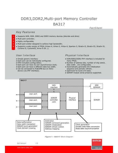
<strong>BA317</strong><br />
SPD<br />
interface<br />
SPD<br />
EEPROM<br />
User <strong>port</strong><br />
User <strong>port</strong><br />
SDRAM<br />
controller<br />
core<br />
Physical<br />
interface<br />
SDRAM<br />
User <strong>port</strong><br />
Data bufferization<br />
Data width translation<br />
SDRAM burst generation<br />
Clock domain crossing<br />
Arbitration<br />
SDRAM command generation<br />
SDRAM initialization<br />
SDRAM refresh control<br />
Address mapping<br />
Clock generation<br />
Double Data Rate conversion<br />
Read data resynchronization<br />
Figure 1 - <strong>BA317</strong> Block Diagram<br />
Doc.Version: 1.5<br />
www.barco-silex.com
General description<br />
The <strong>BA317</strong> is a highly configurable DDR/<strong>DDR2</strong>/<strong>DDR3</strong>-SDRAM <strong>Memory</strong> <strong>Controller</strong> developed, validated &<br />
licensed by BARCO-Silex. It sup<strong>port</strong>s both Single Data Rate (SDR) and Double Data Rate<br />
(DDR/<strong>DDR2</strong>/<strong>DDR3</strong>) SDRAM devices.<br />
The <strong>BA317</strong> is an assembly of modules (controller core, user <strong>port</strong>s and physical interface). According to<br />
the user needs, a top-level can be automatically generated with all modules included.<br />
The controller core includes a multi-<strong>port</strong> arbiter and a command sequencer. It is optimized to achieve<br />
high bandwidth by mixing accesses to the different banks of the SDRAM. It generates burst of 8 data<br />
with auto-precharge option, allowing continuous data transfer in case of long bursts.<br />
The user <strong>port</strong> includes FIFO (for both data and addresses). Each <strong>port</strong> can have a different data bus<br />
width (larger or smaller than the SDRAM bus width). The user <strong>port</strong> provides access to individual data. It<br />
manages the generation of SDRAM burst.<br />
The physical interface manages the double data rate and the source synchronous data sampling.<br />
Technical Description<br />
General Parameters<br />
Parameter<br />
SDRAM Type<br />
SDRAM width<br />
SDRAM addressing<br />
SDRAM timing<br />
SDRAM operating<br />
parameters<br />
DIMM parameters<br />
Arbitration<br />
Serial Presence Detect<br />
Implementation options<br />
User Port Types<br />
Port type<br />
Buffered<br />
IPIF<br />
Video<br />
Raw<br />
General Parameters<br />
Description<br />
SDR, DDR, <strong>DDR2</strong> or <strong>DDR3</strong>.<br />
Data bus width.<br />
Bank address width; Row address width; Column address width.<br />
These parameters can also be dynamically configured (via SPD).<br />
tRCD; tRP; tRAS; tRC; tWR; tRFC; tREFI; tWTR; tRTP; tFAW.<br />
Clock frequency; CAS latency; CWL Latency; Burst length.<br />
Registered or not; Number of chip select; Number of clock pairs.<br />
Number of <strong>port</strong>s; number of consecutive read/write accesses.<br />
Included or not.<br />
Possibility to add some pipeline to increase frequency.<br />
Table 1 - General Parameters<br />
Following user <strong>port</strong>s are available<br />
Description<br />
This is a generic type of <strong>port</strong>. It includes FIFO, clock domain crossing, data bus<br />
width adaptation, SDRAM burst generation.<br />
The IPIF <strong>port</strong> allows interfacing with PLB / OPB bus on Xilinx device. The Xilinx<br />
EDK (Embedded Development Kit) provides the modules plb_ipif and opb_ipif as<br />
interface between PLB / OPB and IPIF.<br />
The video <strong>port</strong>s allow a direct connection to the J2K IP’s of <strong>Barco</strong>-Silex.<br />
The raw <strong>port</strong> provides direct access to the controller core. No FIFO is included, no<br />
clock domain crossing is sup<strong>port</strong>ed, and access is burst based.<br />
Table 2 – User Port Types<br />
Page 2 of 4<br />
Technical specifications are subject to change without prior notice
User Port Parameters<br />
User <strong>port</strong> parameters (each <strong>port</strong> can be individually configured)<br />
Parameter<br />
Description<br />
Port type<br />
Port direction<br />
Data bus<br />
Data mask<br />
Clock<br />
FIFO<br />
Acknowledge<br />
Priority<br />
Buffered, IPIF, Digital Cinema or raw.<br />
Read only, write only or read/write.<br />
Data width is configurable.<br />
It is possible to write single byte using data mask.<br />
Asynchronous or synchronous clock.<br />
FIFO depth is configurable.<br />
Optional acknowledge signal can be generated.<br />
Each <strong>port</strong> can have high or low priority.<br />
Table 3 – User Port Parameters<br />
SDRAM PHY interfaces<br />
Following PHY interface are available<br />
FPGA<br />
Description<br />
Virtex-4, Virtex-5<br />
Based on IDELAY.<br />
Automatic delay calibration phase at startup.<br />
Virtex-6<br />
Based on Xilinx PHY module<br />
With automatic calibration phase at startup<br />
Spartan-3…<br />
Based on feedback clock.<br />
Stratix-II, Cyclone-II… Based on feedback clock.<br />
Stratix-II<br />
Stratix-III, Stratix-IV, Cyclone-<br />
III, Arria-II GX<br />
Cyclone-III, Cyclone-IV, Stratix-<br />
III, Stratix-IV<br />
Based on Altera legacy datapath.<br />
Based on Altera non-AFI altmemphy module.<br />
With automatic calibration phase at startup.<br />
Based on Altera AFI altmemphy module.<br />
With automatic calibration phase at startup.<br />
Table 4 – SDRAM PHY Interface<br />
Deliverables<br />
● Compiled model available on request for evaluation;<br />
● RTL/VHDL/Synchronous Design;<br />
● TestBench;<br />
● Documentation.<br />
Implementation Data<br />
● The maximum frequency on the physical side depends mainly on the target technology.<br />
● The maximum frequency on user <strong>port</strong> side depends on the target technology and on the <strong>port</strong><br />
parameters.<br />
● The design area varies largely according to the number of <strong>port</strong>s, the FIFO depth and the data bus<br />
width.<br />
Maturity<br />
● The <strong>BA317</strong> has already been used successfully in many projects, using various FPGA.<br />
Signals description<br />
Refer to the datasheet document for a more detailed description.<br />
Page 3 of 4<br />
Technical specifications are subject to change without prior notice
<strong>Barco</strong> Silex overview<br />
<strong>Barco</strong> Silex is a micro-electronic design house located in Belgium and France belonging to the Belgian<br />
<strong>Barco</strong> group.<br />
<strong>Barco</strong> Silex offers a complete <strong>port</strong>folio of high-end design services, from ASIC/FPGA design to advanced<br />
SoC/SoPC based system development, IP-core design and board design in the fields of:<br />
<br />
<br />
<br />
<br />
Image processing<br />
Communications<br />
Consumer electronics<br />
Industrial electronics.<br />
<strong>Barco</strong> Silex IP products<br />
<strong>Barco</strong> Silex design expertise is also made available through a wide <strong>port</strong>folio of IP products, with a strong<br />
focus on high performance, standardized image processing and encryption functions.<br />
All these IP cores have been designed and fully validated by <strong>Barco</strong> Silex and are hardware proven,<br />
which guarantees high IP quality as well as best sup<strong>port</strong> during your integration phase.<br />
Deliverables include:<br />
RTL Code or netlist (depending on license type)<br />
Functional simulation testbench<br />
Synthesis script<br />
Full documentation<br />
For some of them, we can also provide you with simulation models and a design kit.<br />
These "off the shelf", high quality IP cores provide you with the fastest and most efficient way of<br />
integrating complex functionalities on FPGAs or ASICs, while meeting short time to market constraints.<br />
More information<br />
Order-reference: <strong>BA317</strong><br />
For additional information and other IP products contact:<br />
<strong>Barco</strong> – Silex<br />
e-mail: barco-silex@barco.com<br />
http://www.barco-silex.com<br />
Or contact the local <strong>Barco</strong> Silex design centers:<br />
Belgium France France<br />
Scientific Park ZI Peynier- Rousset 171b, Av.du Gal De Gaulle<br />
Rue du Bosquet 7 Route de Trets Imm CCE Bat C<br />
1348 Louvain-la Neuve 13790 Peynier 92200 Neuilly sur Seine<br />
+32(0)10/45.49.04 +33 1 47 38 30 89 +33 1 47 38 30 89<br />
Page 4 of 4<br />
Technical specifications are subject to change without prior notice