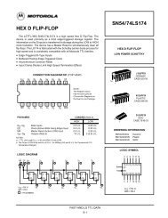
LM6171 High Speed Low Power Low Distortion Voltage ... - Micropik
LM6171 High Speed Low Power Low Distortion Voltage ... - Micropik
LM6171 High Speed Low Power Low Distortion Voltage ... - Micropik

You also want an ePaper? Increase the reach of your titles
YUMPU automatically turns print PDFs into web optimized ePapers that Google loves.
<strong>LM6171</strong><br />
±5V AC Electrical Characteristics (Continued)<br />
Unless otherwise specified, all limits guaranteed for T J = 25˚C, V + = +5V, V − = −5V, V CM = 0V, and R L =1kΩ. Boldface<br />
limits apply at the temperature extremes<br />
Typ <strong>LM6171</strong>AI <strong>LM6171</strong>BI<br />
Symbol Parameter Conditions (Note 5) Limit Limit Units<br />
(Note 6) (Note 6)<br />
Propagation Delay V IN = ±1V, R L = 500Ω, 8 ns<br />
A V =−2<br />
A D Differential Gain (Note 10) 0.04 %<br />
φ D Differential Phase (Note 10) 0.7 deg<br />
e n Input-Referred f = 1 kHz 11<br />
<strong>Voltage</strong> Noise<br />
i n Input-Referred f = 1 kHz 1<br />
Current Noise<br />
Note 1: Absolute Maximum Ratings indicate limits beyond which damage to the device may occur. Operating Ratings indicate conditions for which the device is<br />
intended to be functional, but specific performance is not guaranteed. For guaranteed specifications and the test conditions, see the Electrical Characteristics.<br />
Note 2: Human body model, 1.5 kΩ in series with 100 pF.<br />
Note 3: Continuous short circuit operation at elevated ambient temperature can result in exceeding the maximum allowed junction temperature of 150˚C.<br />
Note 4: The maximum power dissipation is a function of T J(max) , θ JA , and T A . The maximum allowable power dissipation at any ambient temperature is P D =<br />
(T J(max) − T A )/θ JA . All numbers apply for packages soldered directly into a PC board.<br />
Note 5: Typical Values represent the most likely parametric norm.<br />
Note 6: All limits are guaranteed by testing or statistical analysis.<br />
Note 7: Large signal voltage gain is the total output swing divided by the input signal required to produce that swing. For V S = ±15V, V OUT = ±5V. For V S = +5V,<br />
V OUT = ±1V.<br />
Note 8: The open loop output current is the output swing with the 100Ω load resistor divided by that resistor.<br />
Note 9: Slew rate is the average of the rising and falling slew rates.<br />
Note 10: Differential gain and phase are measured with A V = +2, V IN =1V PP at 3.58 MHz and both input and output 75Ω terminated.<br />
www.national.com 6