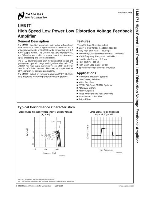
LM6171 High Speed Low Power Low Distortion Voltage ... - Micropik
LM6171 High Speed Low Power Low Distortion Voltage ... - Micropik
LM6171 High Speed Low Power Low Distortion Voltage ... - Micropik

You also want an ePaper? Increase the reach of your titles
YUMPU automatically turns print PDFs into web optimized ePapers that Google loves.
<strong>LM6171</strong><br />
<strong>High</strong> <strong>Speed</strong> <strong>Low</strong> <strong>Power</strong> <strong>Low</strong> <strong>Distortion</strong> <strong>Voltage</strong> Feedback<br />
Amplifier<br />
General Description<br />
The <strong>LM6171</strong> is a high speed unity-gain stable voltage feedback<br />
amplifier. It offers a high slew rate of 3600V/µs and a<br />
unity-gain bandwidth of 100 MHz while consuming only 2.5<br />
mA of supply current. The <strong>LM6171</strong> has very impressive AC<br />
and DC performance which is a great benefit for high speed<br />
signal processing and video applications.<br />
The ±15V power supplies allow for large signal swings and<br />
give greater dynamic range and signal-to-noise ratio. The<br />
<strong>LM6171</strong> has high output current drive, low SFDR and THD,<br />
ideal for ADC/DAC systems. The <strong>LM6171</strong> is specified for<br />
±5V operation for portable applications.<br />
The <strong>LM6171</strong> is built on National’s advanced VIP III (Vertically<br />
Integrated PNP) complementary bipolar process.<br />
Typical Performance Characteristics<br />
Closed Loop Frequency Responsevs. Supply <strong>Voltage</strong><br />
(A V = +1)<br />
Features<br />
(Typical Unless Otherwise Noted)<br />
n Easy-To-Use <strong>Voltage</strong> Feedback Topology<br />
n Very <strong>High</strong> Slew Rate: 3600V/µs<br />
n Wide Unity-Gain-Bandwidth Product: 100 MHz<br />
n −3dB Frequency @ A V = +2: 62 MHz<br />
n <strong>Low</strong> Supply Current: 2.5 mA<br />
n <strong>High</strong> CMRR: 110 dB<br />
n <strong>High</strong> Open Loop Gain: 90 dB<br />
n Specified for ±15V and ±5V Operation<br />
Applications<br />
n Multimedia Broadcast Systems<br />
n Line Drivers, Switchers<br />
n Video Amplifiers<br />
n NTSC, PAL ® and SECAM Systems<br />
n ADC/DAC Buffers<br />
n HDTV Amplifiers<br />
n Pulse Amplifiers and Peak Detectors<br />
n Instrumentation Amplifier<br />
n Active Filters<br />
Large Signal Pulse Response<br />
A V = +1, V S = ±15<br />
February 2003<br />
<strong>LM6171</strong> <strong>High</strong> <strong>Speed</strong> <strong>Low</strong> <strong>Power</strong> <strong>Low</strong> <strong>Distortion</strong> <strong>Voltage</strong> Feedback Amplifier<br />
01233609<br />
01233605<br />
VIP is a trademark of National Semiconductor Corporation.<br />
PAL ® is a registered trademark of and used under licence from Advanced Micro Devices, Inc.<br />
© 2003 National Semiconductor Corporation DS012336 www.national.com
<strong>LM6171</strong><br />
Connection Diagram<br />
8-Pin DIP/SO<br />
Top View<br />
01233601<br />
Ordering Information<br />
Package Temperature Range Transport Media NSC Drawing<br />
Industrial<br />
−40˚C to +85˚C<br />
8-Pin <strong>LM6171</strong>AIN Rails N08E<br />
Molded DIP <strong>LM6171</strong>BIN<br />
8-Pin <strong>LM6171</strong>AIM, <strong>LM6171</strong>BIM Rails M08A<br />
Small Outline <strong>LM6171</strong>AIMX, <strong>LM6171</strong>BIMX 2.5k Units Tape and Reel<br />
www.national.com 2
Absolute Maximum Ratings (Note 1)<br />
If Military/Aerospace specified devices are required,<br />
please contact the National Semiconductor Sales Office/<br />
Distributors for availability and specifications.<br />
ESD Tolerance (Note 2)<br />
2.5 kV<br />
Supply <strong>Voltage</strong> (V + –V − )<br />
36V<br />
Differential Input <strong>Voltage</strong> ±10V<br />
Common-Mode <strong>Voltage</strong> Range V + +0.3V to V − −0.3V<br />
Input Current<br />
±10mA<br />
Output Short Circuit to Ground<br />
(Note 3)<br />
Continuous<br />
Storage Temperature Range<br />
−65˚C to +150˚C<br />
Maximum Junction Temperature<br />
(Note 4)<br />
150˚C<br />
Soldering Information<br />
Infrared or Convection Reflow<br />
(20 sec.) 235˚C<br />
Wave Soldering Lead Temp<br />
(10 sec.) 260˚C<br />
Operating Ratings (Note 1)<br />
Supply <strong>Voltage</strong><br />
Operating Temperature Range<br />
<strong>LM6171</strong>AI, <strong>LM6171</strong>BI<br />
Thermal Resistance (θ JA )<br />
N Package, 8-Pin Molded DIP<br />
M Package, 8-Pin Surface Mount<br />
5.5V ≤ V S ≤ 34V<br />
−40˚C to +85˚C<br />
108˚C/W<br />
172˚C/W<br />
<strong>LM6171</strong><br />
±15V DC Electrical Characteristics<br />
Unless otherwise specified, all limits guaranteed for T J = 25˚C, V + = +15V, V − = −15V, V CM = 0V, and R L =1kΩ. Boldface<br />
limits apply at the temperature extremes<br />
Typ <strong>LM6171</strong>AI <strong>LM6171</strong>BI<br />
Symbol Parameter Conditions (Note 5) Limit Limit Units<br />
(Note 6) (Note 6)<br />
V OS Input Offset <strong>Voltage</strong> 1.5 3 6 mV<br />
5 8 max<br />
TC V OS Input Offset <strong>Voltage</strong> Average Drift 6 µV/˚C<br />
I B Input Bias Current 1 3 3 µA<br />
4 4 max<br />
I OS Input Offset Current 0.03 2 2 µA<br />
3 3 max<br />
R IN Input Resistance Common Mode 40 MΩ<br />
Differential Mode 4.9<br />
R O Open Loop 14 Ω<br />
Output Resistance<br />
CMRR Common Mode V CM = ±10V 110 80 75 dB<br />
Rejection Ratio 75 70 min<br />
PSRR <strong>Power</strong> Supply V S = ±15V to ±5V 95 85 80 dB<br />
Rejection Ratio 80 75 min<br />
V CM Input Common-Mode CMRR ≥ 60 dB ±13.5 V<br />
<strong>Voltage</strong> Range<br />
A V Large Signal <strong>Voltage</strong> R L =1kΩ 90 80 80 dB<br />
Gain (Note 7) 70 70 min<br />
R L = 100Ω 83 70 70 dB<br />
60 60 min<br />
V O Output Swing R L =1kΩ 13.3 12.5 12.5 V<br />
12 12 min<br />
−13.3 −12.5 −12.5 V<br />
−12 −12 max<br />
R L = 100Ω 11.6 9 9 V<br />
8.5 8.5 min<br />
−10.5 −9 −9 V<br />
−8.5 −8.5 max<br />
Continuous Output Current Sourcing, R L = 100Ω 116 90 90 mA<br />
(Open Loop) (Note 8) 85 85 min<br />
3<br />
www.national.com
<strong>LM6171</strong><br />
±15V DC Electrical Characteristics (Continued)<br />
Unless otherwise specified, all limits guaranteed for T J = 25˚C, V + = +15V, V − = −15V, V CM = 0V, and R L =1kΩ. Boldface<br />
limits apply at the temperature extremes<br />
Typ <strong>LM6171</strong>AI <strong>LM6171</strong>BI<br />
Symbol Parameter Conditions (Note 5) Limit Limit Units<br />
(Note 6) (Note 6)<br />
Sinking, R L = 100Ω 105 90 90 mA<br />
85 85 max<br />
Continuous Output Current Sourcing, R L =10Ω 100 mA<br />
(in Linear Region) Sinking, R L =10Ω 80 mA<br />
I SC Output Short Sourcing 135 mA<br />
Circuit Current Sinking 135 mA<br />
I S Supply Current 2.5 4 4 mA<br />
4.5 4.5 max<br />
±15V AC Electrical Characteristics<br />
Unless otherwise specified, all limits guaranteed for T J = 25˚C, V + = +15V, V − = −15V, V CM = 0V, and R L =1kΩ. Boldface<br />
limits apply at the temperature extremes<br />
Typ <strong>LM6171</strong>AI <strong>LM6171</strong>BI<br />
Symbol Parameter Conditions (Note 5) Limit Limit Units<br />
(Note 6) (Note 6)<br />
SR Slew Rate (Note 9) A V = +2, V IN =13V PP 3600 V/µs<br />
A V = +2, V IN =10V PP 3000<br />
GBW Unity Gain-Bandwidth Product 100 MHz<br />
−3 dB Frequency A V = +1 160 MHz<br />
A V = +2 62 MHz<br />
φm Phase Margin 40 deg<br />
t s Settling Time (0.1%) A V = −1, V OUT = ±5V 48 ns<br />
R L = 500Ω<br />
Propagation Delay V IN = ±5V, R L = 500Ω, 6 ns<br />
A V =−2<br />
A D Differential Gain (Note 10) 0.03 %<br />
φ D Differential Phase (Note 10) 0.5 deg<br />
e n Input-Referred f = 1 kHz 12<br />
<strong>Voltage</strong> Noise<br />
i n Input-Referred f = 1 kHz 1<br />
Current Noise<br />
±5V DC Electrical Characteristics<br />
Unless otherwise specified, all limits guaranteed for T J = 25˚C, V + = +5V, V − = −5V, V CM = 0V, and R L =1kΩ. Boldface limits<br />
apply at the temperature extremes<br />
Typ <strong>LM6171</strong>AI <strong>LM6171</strong>BI<br />
Symbol Parameter Conditions (Note 5) Limit Limit Units<br />
(Note 6) (Note 6)<br />
V OS Input Offset <strong>Voltage</strong> 1.2 3 6 mV<br />
5 8 max<br />
TC V OS Input Offset <strong>Voltage</strong> 4 µV/˚C<br />
Average Drift<br />
I B Input Bias Current 1 2.5 2.5 µA<br />
3.5 3.5 max<br />
I OS Input Offset Current 0.03 1.5 1.5 µA<br />
www.national.com 4
±5V DC Electrical Characteristics (Continued)<br />
Unless otherwise specified, all limits guaranteed for T J = 25˚C, V + = +5V, V − = −5V, V CM = 0V, and R L =1kΩ. Boldface limits<br />
apply at the temperature extremes<br />
Typ <strong>LM6171</strong>AI <strong>LM6171</strong>BI<br />
Symbol Parameter Conditions (Note 5) Limit Limit Units<br />
(Note 6) (Note 6)<br />
2.2 2.2 max<br />
R IN Input Resistance Common Mode 40 MΩ<br />
Differential Mode 4.9<br />
R O Open Loop 14 Ω<br />
Output Resistance<br />
CMRR Common Mode V CM = ±2.5V 105 80 75 dB<br />
Rejection Ratio 75 70 min<br />
PSRR <strong>Power</strong> Supply V S = ±15V to ±5V 95 85 80 dB<br />
Rejection Ratio 80 75 min<br />
V CM Input Common-Mode CMRR ≥ 60 dB ±3.7 V<br />
<strong>Voltage</strong> Range<br />
A V Large Signal <strong>Voltage</strong> R L =1kΩ 84 75 75 dB<br />
Gain (Note 7) 65 65 min<br />
R L = 100Ω 80 70 70 dB<br />
60 60 min<br />
V O Output Swing R L =1kΩ 3.5 3.2 3.2 V<br />
3 3 min<br />
−3.4 −3.2 −3.2 V<br />
−3 −3 max<br />
R L = 100Ω 3.2 2.8 2.8 V<br />
2.5 2.5 min<br />
−3.0 −2.8 −2.8 V<br />
−2.5 −2.5 max<br />
Continuous Output Current Sourcing, R L = 100Ω 32 28 28 mA<br />
(Open Loop) (Note 8) 25 25 min<br />
Sinking, R L = 100Ω 30 28 28 mA<br />
25 25 max<br />
I SC Output Short Sourcing 130 mA<br />
Circuit Current Sinking 100 mA<br />
I S Supply Current 2.3 3 3 mA<br />
3.5 3.5 max<br />
<strong>LM6171</strong><br />
±5V AC Electrical Characteristics<br />
Unless otherwise specified, all limits guaranteed for T J = 25˚C, V + = +5V, V − = −5V, V CM = 0V, and R L =1kΩ. Boldface<br />
limits apply at the temperature extremes<br />
Typ <strong>LM6171</strong>AI <strong>LM6171</strong>BI<br />
Symbol Parameter Conditions (Note 5) Limit Limit Units<br />
(Note 6) (Note 6)<br />
SR Slew Rate (Note 9) A V = +2, V IN = 3.5 V PP 750 V/µs<br />
GBW Unity Gain-Bandwidth 70 MHz<br />
Product<br />
−3 dB Frequency A V = +1 130 MHz<br />
A V =+2 45<br />
φm Phase Margin 57 deg<br />
t s Settling Time (0.1%) A V = −1, V OUT = +1V, 60 ns<br />
R L = 500Ω<br />
5<br />
www.national.com
<strong>LM6171</strong><br />
±5V AC Electrical Characteristics (Continued)<br />
Unless otherwise specified, all limits guaranteed for T J = 25˚C, V + = +5V, V − = −5V, V CM = 0V, and R L =1kΩ. Boldface<br />
limits apply at the temperature extremes<br />
Typ <strong>LM6171</strong>AI <strong>LM6171</strong>BI<br />
Symbol Parameter Conditions (Note 5) Limit Limit Units<br />
(Note 6) (Note 6)<br />
Propagation Delay V IN = ±1V, R L = 500Ω, 8 ns<br />
A V =−2<br />
A D Differential Gain (Note 10) 0.04 %<br />
φ D Differential Phase (Note 10) 0.7 deg<br />
e n Input-Referred f = 1 kHz 11<br />
<strong>Voltage</strong> Noise<br />
i n Input-Referred f = 1 kHz 1<br />
Current Noise<br />
Note 1: Absolute Maximum Ratings indicate limits beyond which damage to the device may occur. Operating Ratings indicate conditions for which the device is<br />
intended to be functional, but specific performance is not guaranteed. For guaranteed specifications and the test conditions, see the Electrical Characteristics.<br />
Note 2: Human body model, 1.5 kΩ in series with 100 pF.<br />
Note 3: Continuous short circuit operation at elevated ambient temperature can result in exceeding the maximum allowed junction temperature of 150˚C.<br />
Note 4: The maximum power dissipation is a function of T J(max) , θ JA , and T A . The maximum allowable power dissipation at any ambient temperature is P D =<br />
(T J(max) − T A )/θ JA . All numbers apply for packages soldered directly into a PC board.<br />
Note 5: Typical Values represent the most likely parametric norm.<br />
Note 6: All limits are guaranteed by testing or statistical analysis.<br />
Note 7: Large signal voltage gain is the total output swing divided by the input signal required to produce that swing. For V S = ±15V, V OUT = ±5V. For V S = +5V,<br />
V OUT = ±1V.<br />
Note 8: The open loop output current is the output swing with the 100Ω load resistor divided by that resistor.<br />
Note 9: Slew rate is the average of the rising and falling slew rates.<br />
Note 10: Differential gain and phase are measured with A V = +2, V IN =1V PP at 3.58 MHz and both input and output 75Ω terminated.<br />
www.national.com 6
Typical Performance Characteristics Unless otherwise noted, T A = 25˚C<br />
Supply Current vs. Supply <strong>Voltage</strong><br />
Supply Current vs. Temperature<br />
<strong>LM6171</strong><br />
01233620 01233621<br />
Input Offset <strong>Voltage</strong> vs. Temperature<br />
Input Bias Current vs. Temperature<br />
01233622<br />
Input Offset <strong>Voltage</strong> vs. Common Mode <strong>Voltage</strong><br />
01233623<br />
Short Circuit Current vs. Temperature (Sourcing)<br />
01233624<br />
01233625<br />
7<br />
www.national.com
<strong>LM6171</strong><br />
Typical Performance Characteristics Unless otherwise noted, T A = 25˚C (Continued)<br />
Short Circuit Current vs. Temperature (Sinking)<br />
Output <strong>Voltage</strong> vs. Output Current<br />
01233626<br />
01233627<br />
Output <strong>Voltage</strong> vs. Output Current<br />
CMRR vs. Frequency<br />
01233628<br />
01233629<br />
PSRR vs. Frequency<br />
PSRR vs. Frequency<br />
01233630 01233631<br />
www.national.com 8
Typical Performance Characteristics Unless otherwise noted, T A = 25˚C (Continued)<br />
Open Loop Frequency Response<br />
Open Loop Frequency Response<br />
<strong>LM6171</strong><br />
01233632<br />
Gain Bandwidth Product vs. Supply <strong>Voltage</strong><br />
01233633<br />
Gain Bandwidth Product vs. Load Capacitance<br />
01233634<br />
Large Signal <strong>Voltage</strong> Gain vs. Load<br />
01233635<br />
Large Signal <strong>Voltage</strong> Gain vs. Load<br />
01233636 01233637<br />
9<br />
www.national.com
<strong>LM6171</strong><br />
Typical Performance Characteristics Unless otherwise noted, T A = 25˚C (Continued)<br />
Input <strong>Voltage</strong> Noise vs. Frequency<br />
Input <strong>Voltage</strong> Noise vs. Frequency<br />
01233638 01233639<br />
Input Current Noise vs. Frequency<br />
Input Current Noise vs. Frequency<br />
01233640 01233641<br />
Slew Rate vs. Supply <strong>Voltage</strong><br />
Slew Rate vs. Input <strong>Voltage</strong><br />
01233642<br />
01233643<br />
www.national.com 10
Typical Performance Characteristics Unless otherwise noted, T A = 25˚C (Continued)<br />
Slew Rate vs. Load Capacitance<br />
Open Loop Output Impedance vs. Frequency<br />
<strong>LM6171</strong><br />
01233644 01233645<br />
Open Loop Output Impedance vs. Frequency<br />
Large Signal Pulse Response<br />
A V = −1, V S = ±15V<br />
01233647<br />
01233646<br />
Large Signal Pulse Response<br />
A V = −1, V S = ±5V<br />
Large Signal Pulse Response<br />
A V = +1, V S = ±15V<br />
01233648 01233649<br />
11<br />
www.national.com
<strong>LM6171</strong><br />
Typical Performance Characteristics Unless otherwise noted, T A = 25˚C (Continued)<br />
Large Signal Pulse Response<br />
A V = +1, V S = ±5V<br />
Large Signal Pulse Response<br />
A V = +2, V S = ±15V<br />
01233650 01233651<br />
Large Signal Pulse Response<br />
A V = +2, V S = ±5V<br />
Small Signal Pulse Response<br />
A V = −1, V S = ±15V<br />
01233652 01233653<br />
Small Signal Pulse Response<br />
A V = −1, V S = ±5V<br />
Small Signal Pulse Response<br />
A V = +1, V S = ±15V<br />
01233654 01233655<br />
www.national.com 12
Typical Performance Characteristics Unless otherwise noted, T A = 25˚C (Continued)<br />
Small Signal Pulse Response<br />
A V = +1, V S = ±5V<br />
Small Signal Pulse Response<br />
A V = +2, V S = ±15V<br />
<strong>LM6171</strong><br />
01233656 01233657<br />
Small Signal Pulse Response<br />
A V = +2, V S = ±5V<br />
Closed Loop Frequency Response vs. Supply<strong>Voltage</strong><br />
(A V = +1)<br />
01233658<br />
01233659<br />
Closed Loop Frequency Response vs. Supply <strong>Voltage</strong><br />
(A V = +2)<br />
Closed Loop Frequency Response vs. Capacitive Load<br />
(A V = +1)<br />
01233660 01233661<br />
13<br />
www.national.com
<strong>LM6171</strong><br />
Typical Performance Characteristics Unless otherwise noted, T A = 25˚C (Continued)<br />
Closed Loop Frequency Response vs. Capacitive Load<br />
(A V = +1)<br />
Closed Loop Frequency Response vs. Capacitive Load<br />
(A V = +2)<br />
01233662<br />
01233663<br />
Closed Loop Frequency Response vs. Capacitive Load<br />
(A V = +2) Total Harmonic <strong>Distortion</strong> vs. Frequency<br />
01233664 01233665<br />
Total Harmonic <strong>Distortion</strong> vs. Frequency<br />
Total Harmonic <strong>Distortion</strong> vs. Frequency<br />
01233666 01233667<br />
www.national.com 14
Typical Performance Characteristics Unless otherwise noted, T A = 25˚C (Continued)<br />
Total Harmonic <strong>Distortion</strong> vs. Frequency<br />
Undistorted Output Swing vs. Frequency<br />
<strong>LM6171</strong><br />
01233668 01233669<br />
Undistorted Output Swing vs. Frequency<br />
Undistorted Output Swing vs. Frequency<br />
01233670 01233671<br />
Undistorted Output Swing vs. Frequency<br />
Total <strong>Power</strong> Dissipation vs. Ambient Temperature<br />
01233672<br />
01233673<br />
15<br />
www.national.com
<strong>LM6171</strong><br />
<strong>LM6171</strong> Simplified Schematic<br />
01233610<br />
Application Information<br />
<strong>LM6171</strong> PERFORMANCE DISCUSSION<br />
The <strong>LM6171</strong> is a high speed, unity-gain stable voltage feedback<br />
amplifier. It consumes only 2.5 mA supply current while<br />
providing a gain-bandwidth product of 100 MHz and a slew<br />
rate of 3600V/µs. It also has other great features such as low<br />
differential gain and phase and high output current. The<br />
<strong>LM6171</strong> is a good choice in high speed circuits.<br />
The <strong>LM6171</strong> is a true voltage feedback amplifier. Unlike<br />
current feedback amplifiers (CFAs) with a low inverting input<br />
impedance and a high non-inverting input impedance, both<br />
inputs of voltage feedback amplifiers (VFAs) have high impedance<br />
nodes. The low impedance inverting input in CFAs<br />
will couple with feedback capacitor and cause oscillation. As<br />
a result, CFAs cannot be used in traditional op amp circuits<br />
such as photodiode amplifiers, I-to-V converters and integrators.<br />
<strong>LM6171</strong> CIRCUIT OPERATION<br />
The class AB input stage in <strong>LM6171</strong> is fully symmetrical and<br />
has a similar slewing characteristic to the current feedback<br />
amplifiers. In the <strong>LM6171</strong> Simplfied Schematic, Q1 through<br />
Q4 form the equivalent of the current feedback input buffer,<br />
R E the equivalent of the feedback resistor, and stage A<br />
buffers the inverting input. The triple-buffered output stage<br />
isolates the gain stage from the load to provide low output<br />
impedance.<br />
<strong>LM6171</strong> SLEW RATE CHARACTERISTIC<br />
The slew rate of <strong>LM6171</strong> is determined by the current available<br />
to charge and discharge an internal high impedance<br />
node capacitor. The current is the differential input voltage<br />
divided by the total degeneration resistor R E . Therefore, the<br />
slew rate is proportional to the input voltage level, and the<br />
higher slew rates are achievable in the lower gain configurations.<br />
When a very fast large signal pulse is applied to the input of<br />
an amplifier, some overshoot or undershoot occurs. By placing<br />
an external series resistor such as 1 kΩ to the input of<br />
<strong>LM6171</strong>, the bandwidth is reduced to help lower the overshoot.<br />
LAYOUT CONSIDERATION<br />
Printed Circuit Boards and <strong>High</strong> <strong>Speed</strong> Op Amps<br />
There are many things to consider when designing PC<br />
boards for high speed op amps. Without proper caution, it is<br />
very easy and frustrating to have excessive ringing, oscillation<br />
and other degraded AC performance in high speed<br />
circuits. As a rule, the signal traces should be short and wide<br />
to provide low inductance and low impedance paths. Any<br />
unused board space needs to be grounded to reduce stray<br />
signal pickup. Critical components should also be grounded<br />
at a common point to eliminate voltage drop. Sockets add<br />
capacitance to the board and can affect frequency performance.<br />
It is better to solder the amplifier directly into the PC<br />
board without using any socket.<br />
Using Probes<br />
Active (FET) probes are ideal for taking high frequency<br />
measurements because they have wide bandwidth, high<br />
input impedance and low input capacitance. However, the<br />
probe ground leads provide a long ground loop that will<br />
produce errors in measurement. Instead, the probes can be<br />
grounded directly by removing the ground leads and probe<br />
jackets and using scope probe jacks.<br />
Components Selection And Feedback Resistor<br />
It is important in high speed applications to keep all component<br />
leads short because wires are inductive at high frequency.<br />
For discrete components, choose carbon<br />
www.national.com 16
Application Information (Continued)<br />
composition-type resistors and mica-type capacitors. Surface<br />
mount components are preferred over discrete components<br />
for minimum inductive effect.<br />
Large values of feedback resistors can couple with parasitic<br />
capacitance and cause undesirable effects such as ringing<br />
or oscillation in high speed amplifiers. For <strong>LM6171</strong>, a feedback<br />
resistor of 510Ω gives optimal performance.<br />
COMPENSATION FOR INPUT CAPACITANCE<br />
The combination of an amplifier’s input capacitance with the<br />
gain setting resistors adds a pole that can cause peaking or<br />
oscillation. To solve this problem, a feedback capacitor with<br />
a value<br />
C F<br />
> (R G xC IN )/R F<br />
can be used to cancel that pole. For <strong>LM6171</strong>, a feedback<br />
capacitor of 2 pF is recommended. Figure 1 illustrates the<br />
compensation circuit.<br />
TERMINATION<br />
In high frequency applications, reflections occur if signals<br />
are not properly terminated. Figure 3 shows a properly terminated<br />
signal while Figure 4 shows an improperly terminated<br />
signal.<br />
<strong>LM6171</strong><br />
01233614<br />
FIGURE 3. Properly Terminated Signal<br />
01233611<br />
FIGURE 1. Compensating for Input Capacitance<br />
POWER SUPPLY BYPASSING<br />
Bypassing the power supply is necessary to maintain low<br />
power supply impedance across frequency. Both positive<br />
and negative power supplies should be bypassed individually<br />
by placing 0.01 µF ceramic capacitors directly to power<br />
supply pins and 2.2 µF tantalum capacitors close to the<br />
power supply pins.<br />
01233615<br />
FIGURE 4. Improperly Terminated Signal<br />
01233612<br />
FIGURE 2. <strong>Power</strong> Supply Bypassing<br />
17<br />
www.national.com
<strong>LM6171</strong><br />
Application Information (Continued)<br />
To minimize reflection, coaxial cable with matching characteristic<br />
impedance to the signal source should be used. The<br />
other end of the cable should be terminated with the same<br />
value terminator or resistor. For the commonly used cables,<br />
RG59 has 75Ω characteristic impedance, and RG58 has<br />
50Ω characteristic impedance.<br />
DRIVING CAPACITIVE LOADS<br />
Amplifiers driving capacitive loads can oscillate or have ringing<br />
at the output. To eliminate oscillation or reduce ringing,<br />
an isolation resistor can be placed as shown below in Figure<br />
5. The combination of the isolation resistor and the load<br />
capacitor forms a pole to increase stablility by adding more<br />
phase margin to the overall system. The desired performance<br />
depends on the value of the isolation resistor; the<br />
bigger the isolation resistor, the more damped the pulse<br />
response becomes. For <strong>LM6171</strong>, a 50Ω isolation resistor is<br />
recommended for initial evaluation. Figure 6 shows the<br />
<strong>LM6171</strong> driving a 200 pF load with the 50Ω isolation resistor.<br />
FIGURE 5. Isolation Resistor Used<br />
to Drive Capacitive Load<br />
01233613<br />
For example, for the <strong>LM6171</strong> in a SO-8 package, the maximum<br />
power dissipation at 25˚C ambient temperature is<br />
730 mW.<br />
Thermal resistance, θ JA , depends on parameters such as<br />
die size, package size and package material. The smaller<br />
the die size and package, the higher θ JA becomes. The 8-pin<br />
DIP package has a lower thermal resistance (108˚C/W) than<br />
that of 8-pin SO (172˚C/W). Therefore, for higher dissipation<br />
capability, use an 8-pin DIP package.<br />
The total power dissipated in a device can be calculated as:<br />
P D =P Q +P L<br />
P Q is the quiescent power dissipated in a device with no load<br />
connected at the output. P L is the power dissipated in the<br />
device with a load connected at the output; it is not the power<br />
dissipated by the load.<br />
Furthermore,<br />
P Q = supply current x total supply voltage with no load<br />
P L = output current x (voltage difference between<br />
supply voltage and output voltage of the same<br />
supply)<br />
For example, the total power dissipated by the <strong>LM6171</strong> with<br />
V S = ±15V and output voltage of 10V into 1 kΩ load resistor<br />
(one end tied to ground) is<br />
P D =P Q +P L<br />
= (2.5 mA) x (30V) + (10 mA) x (15V − 10V)<br />
=75mW+50mW<br />
= 125 mW<br />
APPLICATION CIRCUITS<br />
Fast Instrumentation Amplifier<br />
01233617<br />
01233616<br />
FIGURE 6. The <strong>LM6171</strong> Driving a 200 pF Load<br />
with a 50Ω Isolation Resistor<br />
POWER DISSIPATION<br />
The maximum power allowed to dissipate in a device is<br />
defined as:<br />
P D =(T J(max) −T A )/θ JA<br />
Where P D is the power dissipation in a device<br />
T J(max) is the maximum junction temperature<br />
T A is the ambient temperature<br />
θ JA is the thermal resistance of a particular package<br />
www.national.com 18
Application Information (Continued)<br />
Multivibrator<br />
Pulse Width Modulator<br />
<strong>LM6171</strong><br />
01233619<br />
01233618<br />
DESIGN KIT<br />
A design kit is available for the <strong>LM6171</strong>. The design kit<br />
contains:<br />
• <strong>High</strong> <strong>Speed</strong> Evaluation Board<br />
• <strong>LM6171</strong> in 8-pin DIP Package<br />
• <strong>LM6171</strong> Datasheet<br />
• Pspice Macromodel Diskette With the <strong>LM6171</strong> Macromodel<br />
• An Amplifier Selection Guide<br />
• <strong>LM6171</strong> in 8-pin DIP Package<br />
• <strong>LM6171</strong> Datasheet<br />
• Pspice Macromodel Diskette With the <strong>LM6171</strong> Macromodel<br />
Contact your local National Semiconductor sales office to<br />
obtain a pitch pack.<br />
PITCH PACK<br />
A pitch pack is available for the <strong>LM6171</strong>. The pitch pack<br />
contains:<br />
• <strong>High</strong> <strong>Speed</strong> Evaluation Board<br />
19<br />
www.national.com
<strong>LM6171</strong><br />
Physical Dimensions inches (millimeters) unless otherwise noted<br />
8-Pin Small Outline Package<br />
NS Package Number M08A<br />
8-Pin Molded DIP Package<br />
NS Package Number N08E<br />
www.national.com 20
LIFE SUPPORT POLICY<br />
Notes<br />
NATIONAL’S PRODUCTS ARE NOT AUTHORIZED FOR USE AS CRITICAL COMPONENTS IN LIFE SUPPORT<br />
DEVICES OR SYSTEMS WITHOUT THE EXPRESS WRITTEN APPROVAL OF THE PRESIDENT AND GENERAL<br />
COUNSEL OF NATIONAL SEMICONDUCTOR CORPORATION. As used herein:<br />
1. Life support devices or systems are devices or<br />
systems which, (a) are intended for surgical implant<br />
into the body, or (b) support or sustain life, and<br />
whose failure to perform when properly used in<br />
accordance with instructions for use provided in the<br />
labeling, can be reasonably expected to result in a<br />
significant injury to the user.<br />
2. A critical component is any component of a life<br />
support device or system whose failure to perform<br />
can be reasonably expected to cause the failure of<br />
the life support device or system, or to affect its<br />
safety or effectiveness.<br />
<strong>LM6171</strong> <strong>High</strong> <strong>Speed</strong> <strong>Low</strong> <strong>Power</strong> <strong>Low</strong> <strong>Distortion</strong> <strong>Voltage</strong> Feedback Amplifier<br />
National Semiconductor<br />
Americas Customer<br />
Support Center<br />
Email: new.feedback@nsc.com<br />
Tel: 1-800-272-9959<br />
www.national.com<br />
National Semiconductor<br />
Europe Customer Support Center<br />
Fax: +49 (0) 180-530 85 86<br />
Email: europe.support@nsc.com<br />
Deutsch Tel: +49 (0) 69 9508 6208<br />
English Tel: +44 (0) 870 24 0 2171<br />
Français Tel: +33 (0) 1 41 91 8790<br />
National Semiconductor<br />
Asia Pacific Customer<br />
Support Center<br />
Fax: +65-6250 4466<br />
Email: ap.support@nsc.com<br />
Tel: +65-6254 4466<br />
National Semiconductor<br />
Japan Customer Support Center<br />
Fax: 81-3-5639-7507<br />
Email: jpn.feedback@nsc.com<br />
Tel: 81-3-5639-7560<br />
National does not assume any responsibility for use of any circuitry described, no circuit patent licenses are implied and National reserves the right at any time without notice to change said circuitry and specifications.