Training ARM CORTEX A9 A9MP SYSTEM DESIGN - Multi Video ...
Training ARM CORTEX A9 A9MP SYSTEM DESIGN - Multi Video ...
Training ARM CORTEX A9 A9MP SYSTEM DESIGN - Multi Video ...
You also want an ePaper? Increase the reach of your titles
YUMPU automatically turns print PDFs into web optimized ePapers that Google loves.
MVD <strong>Training</strong><br />
Jan-10<br />
Course description<br />
Ref : 004868A<br />
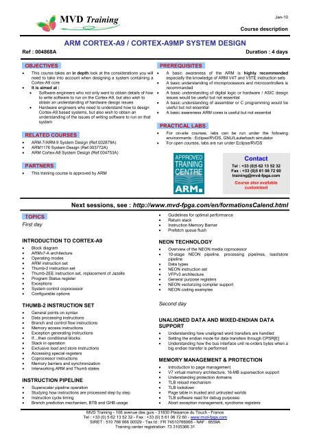
<strong>ARM</strong> <strong>CORTEX</strong>-<strong>A9</strong> / <strong>CORTEX</strong>-<strong>A9</strong>MP <strong>SYSTEM</strong> <strong>DESIGN</strong><br />
Duration : 4 days<br />
OBJECTIVES<br />
• This course takes an in depth look at the considerations you will<br />
need to take into account when designing a system containing a<br />
Cortex-<strong>A9</strong> core<br />
• It is aimed at :<br />
• Software engineers who not only want to obtain details of how<br />
to write software to run on the Cortex-<strong>A9</strong>, but also wish to<br />
obtain an understanding of hardware design issues<br />
• Hardware engineers who need to understand how to design<br />
Cortex-<strong>A9</strong> based systems, but also wish to obtain an<br />
understanding of the issues of writing software to run on that<br />
system<br />
RELATED COURSES<br />
• <strong>ARM</strong>-7/<strong>ARM</strong>-9 System Design (Ref.002879A)<br />
• <strong>ARM</strong>1176 System Design (Ref.003772A)<br />
• <strong>ARM</strong> Cortex-A8 System Design (Ref.004753A)<br />
PARTNERS<br />
• This training course is approved by <strong>ARM</strong><br />
PREREQUISITES<br />
• A basic awareness of the <strong>ARM</strong> is highly recommended<br />
especially the knowledge of <strong>ARM</strong> V4T and V5TE instruction sets<br />
• A basic understanding of microprocessors and microcontrollers is<br />
recommanded<br />
• A basic understanding of digital logic or hardware / ASIC design<br />
issues would be useful but not essential<br />
• A basic understanding of assembler or C programming would be<br />
useful but not essential<br />
• A basic awareness <strong>ARM</strong> cores is useful but not essential<br />
PRACTICAL LABS<br />
• For on-site courses, labs can be run under the following<br />
environments : Eclipse/RVDS, GNU/Lauterbach simulator<br />
• For open courses, labs are run under Eclipse/RVDS<br />
Contact<br />
Tel : +33 (0)5 62 13 52 32<br />
Fax : +33 (0)5 61 06 72 60<br />
training@mvd-fpga.com<br />
Course also available<br />
customized<br />
Next sessions, see : http://www.mvd-fpga.com/en/formationsCalend.html<br />
TOPICS<br />
First day<br />
INTRODUCTION TO <strong>CORTEX</strong>-<strong>A9</strong><br />
• Block diagram<br />
• <strong>ARM</strong>v7-A architecture<br />
• Operating modes<br />
• <strong>ARM</strong> instruction set<br />
• Thumb-2 instruction set<br />
• Thumb-2EE instruction set, replacement of Jazelle<br />
• Program Status register<br />
• Exceptions<br />
• System control coprocessor<br />
• Configurable options<br />
THUMB-2 INSTRUCTION SET<br />
• General points on syntax<br />
• Data processing instructions<br />
• Branch and control flow instructions<br />
• Memory access instructions<br />
• Exception generating instructions<br />
• If…then conditional blocks<br />
• Stack in operation<br />
• Exclusive load and store instructions<br />
• Accessing special registers<br />
• Coprocessor instructions<br />
• Memory barriers and synchronization<br />
• Interworking <strong>ARM</strong> and Thumb states<br />
INSTRUCTION PIPELINE<br />
• Superscalar pipeline operation<br />
• Studying how instructions are processed step by step<br />
• Instruction cycle timing<br />
• Branch prediction mechanism, BTB and GHB usage<br />
• Guidelines for optimal performance<br />
• Return stack<br />
• Instruction Memory Barrier<br />
• Prefetch queue flush<br />
NEON TECHNOLOGY<br />
• Overview of the NEON media coprocessor<br />
• 10-stage NEON pipeline, processing pipelines, load/store<br />
pipeline<br />
• Data types<br />
• NEON instruction set<br />
• VFPv3 architecture<br />
• General purpose registers<br />
• NEON vectorizing compiler support<br />
• NEON coding examples<br />
Second day<br />
UNALIGNED DATA AND MIXED-ENDIAN DATA<br />
SUPPORT<br />
• Understanding how unaligned word transfers are handled<br />
• Setting the endian mode for data transfers through CPSR[E]<br />
• Understanding how the bus interface unit re-orders bytes when a<br />
big endian transfer is performed<br />
MEMORY MANAGEMENT & PROTECTION<br />
• Introduction to page management<br />
• V7 virtual memory architecture, 16-MB supersection support<br />
• Understanding protection domains<br />
• TLB reload mechanism<br />
• TLB lockdown<br />
• Page table in trusted and untrusted worlds<br />
• TLB software read for debug purposes<br />
• Abort exception management, syndrome registers<br />
MVD <strong>Training</strong> - 106 avenue des guis - 31830 Plaisance du Touch - France<br />
Tel : +33 (0) 5 62 13 52 32 - Fax : +33 (0) 5 61 06 72 60 - www.mvd-fpga.com<br />
SIRET : 510 766 066 00029 - Tax Id : FR 74510766066 - NAF : 8559A<br />
<strong>Training</strong> center registration: 73 3105366 31
• Imprecise aborts<br />
MVD <strong>Training</strong><br />
TRUSTZONE<br />
• TrustZone conceptual view<br />
• Secure to non secure permitted transitions<br />
• Related CP15 registers<br />
• L1 and L2 secure state indicators, memory partitioning<br />
HARDWARE IMPLEMENTATION<br />
• Clock domains, CLK, PCLK, ATCLK<br />
• Using clock enable to determine the ratio between input clock<br />
and operation clock<br />
• Reset domains, power-on reset, debug and ETM reset<br />
• Power control, dynamic power management<br />
• Wait For Interrupt architecture<br />
• Debugging the processor while powered down<br />
Third day<br />
LEVEL 1 CACHE<br />
• Cache organization<br />
• Virtual indexing, physical tagging<br />
• Hash Virtual Address Buffer<br />
• Hardware support for virtual aliasing conditions<br />
• Parity protection<br />
• Write buffer<br />
• L1 caches software read for debug purposes<br />
LEVEL 2 CACHE<br />
• Cache organization<br />
• Physical indexing, physical tagging<br />
• L2 cache transfer policy<br />
• Parity / ECC protection<br />
• Write buffer<br />
• L2 Preload Engine [PLE]<br />
• START, STOP and CLEAR commands<br />
• L2 cache software read for debug purposes<br />
MPCore Features<br />
• Snoop Control Unit<br />
• Interrupt Controller<br />
• Timer and Watchdog<br />
• TrustZone support<br />
Developing for <strong>ARM</strong> MPCore Processors<br />
• Booting SMP<br />
• Configuring an interrupt<br />
• Synchronization<br />
• Accelerator Coherency Port<br />
Fourth day<br />
Jan-10<br />
Course description<br />
CORESIGHT DEBUG UNIT<br />
• Coresight specification overview<br />
• CP14 and memory-mapped registers, utilization of an APB slave<br />
interface<br />
• APB port access permissions<br />
• Embedded core debug<br />
• Invasive debug : breakpoints and watchpoints<br />
• Vector catch<br />
• Debug exception<br />
• External debug interface<br />
• Understanding how the Debug unit, the Embedded Trace<br />
Macrocell and the Cross-Triggering Interface interact<br />
CORESIGHT EMBEDDED TRACE MACROCELL<br />
• Overview<br />
• Exporting the compressed trace information<br />
• Benefits of an Embedded Trace Buffer<br />
• Defining trace trigger conditions<br />
• Context ID tracing<br />
• Instrumentation instructions<br />
THE PERFORMANCE MONITOR UNIT<br />
• Event counting principle<br />
• Configuring the 4 event counters<br />
• Event selection<br />
AXI PROTOCOL<br />
• Topology : direct connection, multi-master, multi-layer<br />
• PL300 AXI interconnect<br />
• Separate address/control and data phases<br />
• AXI channels, channel handshake<br />
• Transaction ordering, out of order transaction completion<br />
• Read and write burst timing diagrams<br />
• Cortex-A8 external memory interface, ID encoding<br />
• Exclusive ressource management<br />
APB<br />
• Address decoding stages<br />
• APB interconnect<br />
• APB in AMBA3<br />
DOCUMENTATION<br />
<strong>Training</strong> manuals will be given to attendees during training in print.<br />
MVD <strong>Training</strong> - 106 avenue des guis - 31830 Plaisance du Touch - France<br />
Tel : +33 (0) 5 62 13 52 32 - Fax : +33 (0) 5 61 06 72 60 - www.mvd-fpga.com<br />
SIRET : 510 766 066 00029 - Tax Id : FR 74510766066 - NAF : 8559A<br />
<strong>Training</strong> center registration: 73 3105366 31


