Laboratory Exercise 1 - FTP - Altera
Laboratory Exercise 1 - FTP - Altera
Laboratory Exercise 1 - FTP - Altera

You also want an ePaper? Increase the reach of your titles
YUMPU automatically turns print PDFs into web optimized ePapers that Google loves.
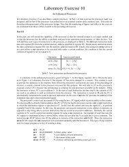
Figure 1. VHDL code that uses the DE2 board switches and lights.<br />
Perform the following steps to implement a circuit corresponding to the code in Figure 1 on the DE2 board.<br />
1. Create a new Quartus II project for your circuit. Select Cyclone II EP2C35F672C6 as the target chip, which<br />
is the FPGA chip on the <strong>Altera</strong> DE2 board.<br />
2. Create a VHDL entity for the code in Figure 1 and include it in your project.<br />
3. Include in your project the required pin assignments for the DE2 board, as discussed above. Compile the<br />
project.<br />
4. Download the compiled circuit into the FPGA chip. Test the functionality of the circuit by toggling the<br />
switches and observing the LEDs.<br />
Part II<br />
Figure 2a shows a sum-of-products circuit that implements a 2-to-1 multiplexer with a select input s. Ifs =0the<br />
multiplexer’s output m is equal to the input x, and if s =1the output is equal to y. Part b of the figure gives a<br />
truth table for this multiplexer, and part c shows its circuit symbol.<br />
x<br />
s<br />
y<br />
m<br />
a) Circuit<br />
s<br />
0<br />
1<br />
m<br />
x<br />
y<br />
s<br />
x<br />
y<br />
0<br />
1<br />
m<br />
b) Truth table c) Symbol<br />
Figure 2. A 2-to-1 multiplexer.<br />
The multiplexer can be described by the following VHDL statement:<br />
m