Laboratory Exercise 1 - FTP - Altera
Laboratory Exercise 1 - FTP - Altera
Laboratory Exercise 1 - FTP - Altera

Create successful ePaper yourself
Turn your PDF publications into a flip-book with our unique Google optimized e-Paper software.
<strong>Laboratory</strong> <strong>Exercise</strong> 1<br />
Switches, Lights, and Multiplexers<br />
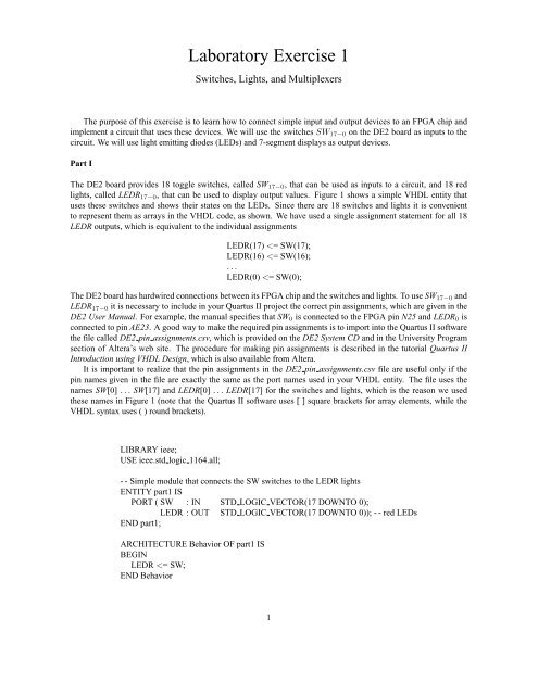
The purpose of this exercise is to learn how to connect simple input and output devices to an FPGA chip and<br />
implement a circuit that uses these devices. We will use the switches SW 17−0 on the DE2 board as inputs to the<br />
circuit. We will use light emitting diodes (LEDs) and 7-segment displays as output devices.<br />
Part I<br />
The DE2 board provides 18 toggle switches, called SW 17−0 , that can be used as inputs to a circuit, and 18 red<br />
lights, called LEDR 17−0 , that can be used to display output values. Figure 1 shows a simple VHDL entity that<br />
uses these switches and shows their states on the LEDs. Since there are 18 switches and lights it is convenient<br />
to represent them as arrays in the VHDL code, as shown. We have used a single assignment statement for all 18<br />
LEDR outputs, which is equivalent to the individual assignments<br />
LEDR(17)
Figure 1. VHDL code that uses the DE2 board switches and lights.<br />
Perform the following steps to implement a circuit corresponding to the code in Figure 1 on the DE2 board.<br />
1. Create a new Quartus II project for your circuit. Select Cyclone II EP2C35F672C6 as the target chip, which<br />
is the FPGA chip on the <strong>Altera</strong> DE2 board.<br />
2. Create a VHDL entity for the code in Figure 1 and include it in your project.<br />
3. Include in your project the required pin assignments for the DE2 board, as discussed above. Compile the<br />
project.<br />
4. Download the compiled circuit into the FPGA chip. Test the functionality of the circuit by toggling the<br />
switches and observing the LEDs.<br />
Part II<br />
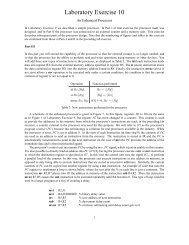
Figure 2a shows a sum-of-products circuit that implements a 2-to-1 multiplexer with a select input s. Ifs =0the<br />
multiplexer’s output m is equal to the input x, and if s =1the output is equal to y. Part b of the figure gives a<br />
truth table for this multiplexer, and part c shows its circuit symbol.<br />
x<br />
s<br />
y<br />
m<br />
a) Circuit<br />
s<br />
0<br />
1<br />
m<br />
x<br />
y<br />
s<br />
x<br />
y<br />
0<br />
1<br />
m<br />
b) Truth table c) Symbol<br />
Figure 2. A 2-to-1 multiplexer.<br />
The multiplexer can be described by the following VHDL statement:<br />
m
s<br />
y 7<br />
0<br />
1<br />
m 7<br />
x 6<br />
y 6<br />
0<br />
1<br />
m 6<br />
s<br />
x 7<br />
0<br />
X<br />
Y<br />
8<br />
8<br />
1<br />
8<br />
M<br />
x 0<br />
y 0<br />
0<br />
1<br />
m 0<br />
a) Circuit b) Symbol<br />
Figure 3. An eight-bit wide 2-to-1 multiplexer.<br />
1. Create a new Quartus II project for your circuit.<br />
2. Include your VHDL file for the eight-bit wide 2-to-1 multiplexer in your project. Use switch SW 17 on the<br />
DE2 board as the s input, switches SW 7−0 as the X input and SW 15−8 as the Y input. Connect the SW<br />
switches to the red lights LEDR and connect the output M to the green lights LEDG 7−0 .<br />
3. Include in your project the required pin assignments for the DE2 board. As discussed in Part I, these<br />
assignments ensure that the input ports of your VHDL code will use the pins on the Cyclone II FPGA<br />
that are connected to the SW switches, and the output ports of your VHDL code will use the FPGA pins<br />
connected to the LEDR and LEDG lights.<br />
4. Compile the project.<br />
5. Download the compiled circuit into the FPGA chip. Test the functionality of the eight-bit wide 2-to-1<br />
multiplexer by toggling the switches and observing the LEDs.<br />
Part III<br />
In Figure 2 we showed a 2-to-1 multiplexer that selects between the two inputs x and y. For this part consider a<br />
circuit in which the output m has to be selected from five inputs u, v, w, x, and y. Part a of Figure 4 shows how<br />
we can build the required 5-to-1 multiplexer by using four 2-to-1 multiplexers. The circuit uses a 3-bit select input<br />
s 2 s 1 s 0 and implements the truth table shown in Figure 4b. A circuit symbol for this multiplexer is given in part c<br />
of the figure.<br />
Recall from Figure 3 that an eight-bit wide 2-to-1 multiplexer can be built by using eight instances of a 2-to-1<br />
multiplexer. Figure 5 applies this concept to define a three-bit wide 5-to-1 multiplexer. It contains three instances<br />
of the circuit in Figure 4a.<br />
3
s 2<br />
s 1<br />
s 0<br />
y<br />
u<br />
v<br />
0<br />
1<br />
0<br />
1<br />
0<br />
1<br />
m<br />
w<br />
x<br />
0<br />
1<br />
a) Circuit<br />
s 2<br />
s 1<br />
s 0 m<br />
0 0 0 u<br />
0 0 1 v<br />
0 1 0 w<br />
0 1 1 x<br />
1 0 0 y<br />
1 0 1 y<br />
1 1 0 y<br />
1 1 1 y<br />
s 2<br />
s 1<br />
s 0<br />
u<br />
v<br />
w<br />
x<br />
y<br />
000<br />
001<br />
010<br />
011<br />
100<br />
m<br />
b) Truth table<br />
c) Symbol<br />
Figure 4. A 5-to-1 multiplexer.<br />
s 2<br />
s 1<br />
s 0<br />
W<br />
U<br />
V<br />
X<br />
3<br />
3<br />
3<br />
3<br />
000<br />
001<br />
010<br />
011<br />
100<br />
3<br />
M<br />
Y<br />
3<br />
Figure 5. A three-bit wide 5-to-1 multiplexer.<br />
Perform the following steps to implement the three-bit wide 5-to-1 multiplexer.<br />
4
1. Create a new Quartus II project for your circuit.<br />
2. Create a VHDL entity for the three-bit wide 5-to-1 multiplexer. Connect its select inputs to switches<br />
SW 17−15 , and use the remaining 15 switches SW 14−0 to provide the five 3-bit inputs U to Y . Connect<br />
the SW switches to the red lights LEDR and connect the output M to the green lights LEDG 2−0 .<br />
3. Include in your project the required pin assignments for the DE2 board. Compile the project.<br />
4. Download the compiled circuit into the FPGA chip. Test the functionality of the three-bit wide 5-to-1<br />
multiplexer by toggling the switches and observing the LEDs. Ensure that each of the inputs U to Y can be<br />
properly selected as the output M.<br />
Part IV<br />
Figure 6 shows a 7-segment decoder module that has the three-bit input c 2 c 1 c 0 . This decoder produces seven<br />
outputs that are used to display a character on a 7-segment display. Table 1 lists the characters that should be<br />
displayed for each valuation of c 2 c 1 c 0 . To keep the design simple, only four characters are included in the table<br />
(plus the ‘blank’ character, which is selected for codes 100 − 111).<br />
The seven segments in the display are identified by the indices 0 to 6 shown in the figure. Each segment is<br />
illuminated by driving it to the logic value 0. You are to write a VHDL entity that implements logic functions that<br />
represent circuits needed to activate each of the seven segments. Use only simple VHDL assignment statements<br />
in your code to specify each logic function using a Boolean expression.<br />
0<br />
c 2<br />
c 1<br />
c 0<br />
7-segment<br />
decoder<br />
5<br />
4<br />
6<br />
1<br />
2<br />
3<br />
Figure 6. A 7-segment decoder.<br />
c 2 c 1 c 0<br />
Character<br />
000 H<br />
001 E<br />
010 L<br />
011 O<br />
100<br />
101<br />
110<br />
111<br />
Table 1. Character codes.<br />
Perform the following steps:<br />
1. Create a new Quartus II project for your circuit.<br />
5
2. Create a VHDL entity for the 7-segment decoder. Connect the c 2 c 1 c 0 inputs to switches SW 2−0 , and connect<br />
the outputs of the decoder to the HEX0 display on the DE2 board. The segments in this display are called<br />
HEX0 0 , HEX0 1 , ..., HEX0 6 , corresponding to Figure 6. You should declare the 7-bit port<br />
HEX0 : OUT STD LOGIC VECTOR(0 TO 6);<br />
in your VHDL code so that the names of these outputs match the corresponding names in the DE2 User<br />
Manual and the DE2 pin assignments.csv file.<br />
3. After making the required DE2 board pin assignments, compile the project.<br />
4. Download the compiled circuit into the FPGA chip. Test the functionality of the circuit by toggling the<br />
SW 2−0 switches and observing the 7-segment display.<br />
Part V<br />
Consider the circuit shown in Figure 7. It uses a three-bit wide 5-to-1 multiplexer to enable the selection of five<br />
characters that are displayed on a 7-segment display. Using the 7-segment decoder from Part IV this circuit can<br />
display any of the characters H, E, L, O, and ‘blank’. The character codes are set according to Table 1 by using<br />
the switches SW 14−0 , and a specific character is selected for display by setting the switches SW 17−15 .<br />
An outline of the VHDL code that represents this circuit is provided in Figure 8. Note that we have used the<br />
circuits from Parts III and IV as subcircuits in this code. You are to extend the code in Figure 8 so that it uses<br />
five 7-segment displays rather than just one. You will need to use five instances of each of the subcircuits. The<br />
purpose of your circuit is to display any word on the five displays that is composed of the characters in Table 1,<br />
and be able to rotate this word in a circular fashion across the displays when the switches SW 17−15 are toggled.<br />
As an example, if the displayed word is HELLO, then your circuit should produce the output patterns illustrated<br />
in Table 2.<br />
SW 17<br />
SW 16<br />
SW 15<br />
SW 14 – 12<br />
SW 11 – 9<br />
SW 8 – 6<br />
SW 5 – 3<br />
SW 2 0<br />
3<br />
3<br />
000<br />
3<br />
001 3 7-segment 7<br />
010<br />
decoder<br />
3<br />
011<br />
100<br />
–<br />
3<br />
5<br />
4<br />
0<br />
6<br />
3<br />
1<br />
2<br />
Figure 7. A circuit that can select and display one of five characters.<br />
6
LIBRARY ieee;<br />
USE ieee.std logic 1164.all;<br />
ENTITY part5 IS<br />
PORT ( SW : IN STD LOGIC VECTOR(17 DOWNTO 0);<br />
HEX0 : OUT STD LOGIC VECTOR(0 TO 6));<br />
END part5;<br />
ARCHITECTURE Behavior OF part5 IS<br />
COMPONENT mux 3bit 5to1<br />
PORT ( S, U, V, W, X, Y : IN STD LOGIC VECTOR(2 DOWNTO 0);<br />
M : OUT STD LOGIC VECTOR(2 DOWNTO 0));<br />
END COMPONENT;<br />
COMPONENT char 7seg<br />
PORT ( C : IN STD LOGIC VECTOR(2 DOWNTO 0);<br />
Display : OUT STD LOGIC VECTOR(0 TO 6));<br />
END COMPONENT;<br />
SIGNAL M : STD LOGIC VECTOR(2 DOWNTO 0);<br />
BEGIN<br />
M0: mux 3bit 5to1 PORT MAP (SW(17 DOWNTO 15), SW(14 DOWNTO 12), SW(11 DOWNTO 9),<br />
SW(8 DOWNTO 6), SW(5 DOWNTO 3), SW(2 DOWNTO 0), M);<br />
H0: char 7seg PORT MAP (M, HEX0);<br />
END Behavior;<br />
LIBRARY ieee;<br />
USE ieee.std logic 1164.all;<br />
- - implements a 3-bit wide 5-to-1 multiplexer<br />
ENTITY mux 3bit 5to1 IS<br />
PORT ( S, U, V, W, X, Y : IN STD LOGIC VECTOR(2 DOWNTO 0);<br />
M : OUT STD LOGIC VECTOR(2 DOWNTO 0));<br />
END mux 3bit 5to1;<br />
ARCHITECTURE Behavior OF mux 3bit 5to1 IS<br />
...code not shown<br />
END Behavior;<br />
LIBRARY ieee;<br />
USE ieee.std logic 1164.all;<br />
ENTITY char 7seg IS<br />
PORT ( C : IN STD LOGIC VECTOR(2 DOWNTO 0);<br />
Display : OUT STD LOGIC VECTOR(0 TO 6));<br />
END char 7seg;<br />
ARCHITECTURE Behavior OF char 7seg IS<br />
...code not shown<br />
END Behavior;<br />
Figure 8. VHDL code for the circuit in Figure 7.<br />
7
SW 17 SW 16 SW 15<br />
Character pattern<br />
000 H E L L O<br />
001 E L L O H<br />
010 L L O H E<br />
011 L O H E L<br />
100 O H E L L<br />
Table 2. Rotating the word HELLO on five displays.<br />
Perform the following steps.<br />
1. Create a new Quartus II project for your circuit.<br />
2. Include your VHDL entity in the Quartus II project. Connect the switches SW 17−15 to the select inputs of<br />
each of the five instances of the three-bit wide 5-to-1 multiplexers. Also connect SW 14−0 to each instance<br />
of the multiplexers as required to produce the patterns of characters shown in Table 2. Connect the outputs<br />
of the five multiplexers to the 7-segment displays HEX4, HEX3, HEX2, HEX1, and HEX0.<br />
3. Include the required pin assignments for the DE2 board for all switches, LEDs, and 7-segment displays.<br />
Compile the project.<br />
4. Download the compiled circuit into the FPGA chip. Test the functionality of the circuit by setting the proper<br />
character codes on the switches SW 14−0 and then toggling SW 17−15 to observe the rotation of the characters.<br />
Part VI<br />
Extend your design from Part V so that is uses all eight 7-segment displays on the DE2 board. Your circuit should<br />
be able to display words with five (or fewer) characters on the eight displays, and rotate the displayed word when<br />
the switches SW 17−15 are toggled. If the displayed word is HELLO, then your circuit should produce the patterns<br />
shown in Table 3.<br />
SW 17 SW 16 SW 15<br />
Character pattern<br />
000 H E L L O<br />
001 H E L L O<br />
010 H E L L O<br />
011 H E L L O<br />
100 E L L O H<br />
101 L L O H E<br />
110 L O H E L<br />
111 O H E L L<br />
Table 3. Rotating the word HELLO on eight displays.<br />
Perform the following steps:<br />
1. Create a new Quartus II project for your circuit and select as the target chip the Cyclone II EP2C35F672C6.<br />
8
2. Include your VHDL entity in the Quartus II project. Connect the switches SW 17−15 to the select inputs of<br />
each instance of the multiplexers in your circuit. Also connect SW 14−0 to each instance of the multiplexers<br />
as required to produce the patterns of characters shown in Table 3. (Hint: for some inputs of the multiplexers<br />
you will want to select the ‘blank’ character.) Connect the outputs of your multiplexers to the 7-segment<br />
displays HEX7, ..., HEX0.<br />
3. Include the required pin assignments for the DE2 board for all switches, LEDs, and 7-segment displays.<br />
Compile the project.<br />
4. Download the compiled circuit into the FPGA chip. Test the functionality of the circuit by setting the proper<br />
character codes on the switches SW 14−0 and then toggling SW 17−15 to observe the rotation of the characters.<br />
Copyright c○2006 <strong>Altera</strong> Corporation.<br />
9