Frequency Synthesizer Design Example
Frequency Synthesizer Design Example
Frequency Synthesizer Design Example

You also want an ePaper? Increase the reach of your titles
YUMPU automatically turns print PDFs into web optimized ePapers that Google loves.
High-speed Serial Interface<br />
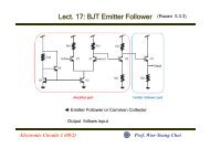
Lect. 11 – Charge-pump PLL 2<br />
1<br />
High-Speed Circuits and Systems Lab., Yonsei University<br />
2013-1
• 2nd order vs. 3rd order<br />
CPPLL<br />
2<br />
High-Speed Circuits and Systems Lab., Yonsei University<br />
2013-1
2nd-order CPPLL<br />
• VCO Control voltage with RC loop filter<br />
– V = V C + V R<br />
<br />
<br />
2013-1<br />
<br />
<br />
<br />
<br />
<br />
<br />
<br />
<br />
Ripples in V during locking process<br />
3<br />
High-Speed Circuits and Systems Lab., Yonsei University
2nd-order CPPLL<br />
• After locking, V should be constant<br />
– But in real PLLs, V fluctuates periodically due to non-ideal effects<br />
– <strong>Example</strong>: Delay mismatch between UP and DOWN path<br />
<br />
<br />
<br />
4<br />
High-Speed Circuits and Systems Lab., Yonsei University<br />
2013-1
3 rd -order CPPLL<br />
• Additional parallel capacitor<br />
– Reduces fluctuation on the control voltage<br />
[rad]<br />
ϕ ref<br />
PD +<br />
Voltage<br />
[I] Loop [V] [rad]<br />
[rad]<br />
Charge<br />
Controlled<br />
Filter<br />
pump<br />
Oscillator<br />
I CP 1<br />
K VCO<br />
R+<br />
2π<br />
( + 1<br />
sC)∥ 1<br />
<br />
s<br />
<br />
ϕ vco<br />
=<br />
Main<br />
Divider<br />
1<br />
M<br />
<br />
2 ( + 1 )∥ 1<br />
<br />
1+ <br />
2 ( + 1 )∥ 1<br />
<br />
<br />
<br />
<br />
<br />
1<br />
<br />
5<br />
=> Additional Pole<br />
High-Speed Circuits and Systems Lab., Yonsei University<br />
2013-1
3 rd -order CPPLL<br />
• Phase margin for 3 rd -order CPPLL<br />
Magnitude [dB]<br />
-40dB/dec<br />
-20dB/dec<br />
Phase [deg]<br />
z LF<br />
GB(Gain=0dB)<br />
p LF<br />
-90<br />
without additional pole<br />
Phase margin<br />
-180<br />
6<br />
High-Speed Circuits and Systems Lab., Yonsei University<br />
2013-1
3 rd -order CPPLL<br />
• <strong>Design</strong> guide for 3 rd -order CPPLL<br />
– For initial damping factor analysis, use 2 nd -order CPPLL<br />
– Rule of thumb: C 1 > 10 x C 2<br />
– For more precise analysis including phase margin,<br />
use behavior simulator: MATLAB, CppSIM<br />
7<br />
High-Speed Circuits and Systems Lab., Yonsei University<br />
2013-1
Input Noise filtering<br />
• Input noise<br />
ϕ noise<br />
PD +<br />
Charge<br />
pump<br />
Loop<br />
Filter<br />
Voltage<br />
Controlled<br />
Oscillator<br />
ϕ out<br />
Main<br />
Divider<br />
– Noise transfer function<br />
= <br />
<br />
=<br />
<br />
2 ( + 1<br />
) <br />
<br />
1+ <br />
2 ( + 1<br />
) <br />
<br />
1<br />
<br />
=<br />
(2 + )/<br />
+2 + <br />
<br />
– Low pass filter for input noise<br />
8<br />
High-Speed Circuits and Systems Lab., Yonsei University<br />
2013-1
Optimal PLL Bandwidth<br />
• Clock generation<br />
– With clean reference clock small input noise<br />
High BW desired<br />
• Clock recovery<br />
– Noisy input<br />
Low BW desired<br />
9<br />
High-Speed Circuits and Systems Lab., Yonsei University<br />
2013-1
VCO Noise<br />
• VCO is not ideal<br />
– Oscillation frequency shifts with time Phase noise<br />
• Single Sideband Noise Spectral Density<br />
= 10<br />
<br />
<br />
10<br />
High-Speed Circuits and Systems Lab., Yonsei University<br />
2013-1
VCO Phase noise<br />
• Phase noise model for VCO<br />
– Leeson's model: single-sideband phase noise in dBc/Hz<br />
= 10 1 2<br />
<br />
2 <br />
<br />
+1<br />
<br />
<br />
+1<br />
<br />
<br />
• where f 0 : output frequency,<br />
Q l : loaded Q<br />
f m : offset from the output frequency (Hz)<br />
f c : 1/f corner frequency<br />
F: noise factor of the amplifier<br />
k: Boltzmann's constant<br />
T: absolute temperature in Kelvins<br />
P s : oscillator output power<br />
11<br />
High-Speed Circuits and Systems Lab., Yonsei University<br />
2013-1
Phase noise<br />
• Phase noise model in VCO<br />
L(f)<br />
Noise floor<br />
f c<br />
f o /2Q L<br />
f offset<br />
12<br />
High-Speed Circuits and Systems Lab., Yonsei University<br />
2013-1
VCO Noise filtering<br />
• VCO phase noise<br />
ϕ noise<br />
ϕ ref<br />
PD +<br />
Charge<br />
pump<br />
Loop<br />
Filter<br />
Voltage<br />
Controlled<br />
Oscillator<br />
ϕ out<br />
Main<br />
Divider<br />
– For noises added after VCO<br />
= <br />
<br />
=<br />
1<br />
1+ <br />
2 ( + 1<br />
) <br />
<br />
1<br />
<br />
=<br />
<br />
+2 + <br />
<br />
High pass filter<br />
13<br />
High-Speed Circuits and Systems Lab., Yonsei University<br />
2013-1
Phase noise<br />
• VCO phase noise filtering<br />
L(f)<br />
Filtering<br />
by PLL<br />
VCO phase noise<br />
Filtered phase noise<br />
f offset<br />
– Optimal PLL Bandwidth<br />
14<br />
High-Speed Circuits and Systems Lab., Yonsei University<br />
2013-1
Phase noise<br />
• Higher bandwidth is better for poor VCO<br />
L(f)<br />
Filtering<br />
by PLL<br />
VCO phase noise<br />
Filtered phase noise<br />
f offset<br />
15<br />
High-Speed Circuits and Systems Lab., Yonsei University<br />
2013-1
Noise filtering<br />
• VCO supply noise<br />
V noise<br />
,<br />
<br />
ϕ ref<br />
PD +<br />
Charge<br />
pump<br />
Loop<br />
Filter<br />
<br />
<br />
VCO<br />
ϕ out<br />
Main<br />
Divider<br />
= <br />
<br />
=<br />
,<br />
<br />
1+ <br />
2 ( + 1<br />
) <br />
<br />
=<br />
1<br />
<br />
, <br />
+2 +<br />
<br />
– 1 zero at DC and 2 poles<br />
Band-pass filter<br />
16<br />
High-Speed Circuits and Systems Lab., Yonsei University<br />
2013-1
Noise filtering<br />
• Noise filtering characteristics<br />
• Many trade-offs for PLL design<br />
Lab project!<br />
17<br />
High-Speed Circuits and Systems Lab., Yonsei University<br />
2013-1
<strong>Frequency</strong> <strong>Synthesizer</strong> <strong>Design</strong> <strong>Example</strong><br />
• Why do we need frequency synthesizer<br />
Sometimes we want to change the clock speed.<br />
Multi-purpose device.<br />
CPU overclocking<br />
Multi-purpose device<br />
High-Speed Circuits and Systems Lab.,Yonsei University 2013-1
<strong>Frequency</strong> <strong>Synthesizer</strong> <strong>Design</strong> <strong>Example</strong><br />
• How to generate a clock signal with a frequency of more than one<br />
Large power & chip area<br />
Low power & chip area<br />
High-Speed Circuits and Systems Lab.,Yonsei University 2013-1
<strong>Frequency</strong> <strong>Synthesizer</strong> <strong>Design</strong> <strong>Example</strong><br />
• Integer-N frequency synthesizer<br />
output clock frequency : N*fref, (N+1)*fref, (N+2)*fref, …<br />
<strong>Frequency</strong> resolution : fref<br />
Hard to have a high frequency resolution..<br />
Ref.<br />
CK<br />
PFD<br />
Charge Pump<br />
V cont<br />
VCO<br />
%N*fref<br />
%N,%2N,%3N,%4N,..<br />
Counter based<br />
frequency divider<br />
Ratio<br />
select<br />
High-Speed Circuits and Systems Lab.,Yonsei University 2013-1
<strong>Frequency</strong> <strong>Synthesizer</strong> <strong>Design</strong> <strong>Example</strong><br />
• Fractional-N frequency synthesizer<br />
output clock frequency : N*fref, (N+0.01)*fref, (N+0.02)*fref, …<br />
<strong>Frequency</strong> resolution : 0.01*fref<br />
Ref.<br />
CK<br />
PFD<br />
Charge Pump<br />
V cont<br />
VCO<br />
%N*fref<br />
%N,%N+0.01,%N+0.02,..<br />
Impossible to<br />
implement<br />
Ratio<br />
select<br />
High-Speed Circuits and Systems Lab.,Yonsei University 2013-1
<strong>Frequency</strong> <strong>Synthesizer</strong> <strong>Design</strong> <strong>Example</strong><br />
• Fractional-N frequency synthesizer<br />
output clock frequency : N*fref, (N+0.01)*fref, (N+0.02)*fref, …<br />
<strong>Frequency</strong> resolution : 0.01*fref<br />
N=45454545…<br />
N avg =4.5<br />
N=44454445…<br />
N avg =4.25<br />
N=45554555…<br />
N avg =4.75<br />
High-Speed Circuits and Systems Lab.,Yonsei University 2013-1
<strong>Frequency</strong> <strong>Synthesizer</strong> <strong>Design</strong> <strong>Example</strong><br />
• Fractional-N frequency synthesizer<br />
Output frequency range : 200MHz ~ 250MHz<br />
<strong>Frequency</strong> resolution : 12.5MHz<br />
Reference clock frequency : 50MHz<br />
High-Speed Circuits and Systems Lab.,Yonsei University 2013-1
<strong>Frequency</strong> <strong>Synthesizer</strong> <strong>Design</strong> <strong>Example</strong><br />
• PFD (Phase and <strong>Frequency</strong> detector) design<br />
Ref.CK and VCO.CK, which one is faster<br />
How fast<br />
Ref.CK<br />
VCO.CK<br />
Lead<br />
Lag<br />
Reset<br />
Phase difference = Lead pulse area – Lag pulse area<br />
High-Speed Circuits and Systems Lab.,Yonsei University 2013-1
<strong>Frequency</strong> <strong>Synthesizer</strong> <strong>Design</strong> <strong>Example</strong><br />
• Charge pump design<br />
With loop filter, it works as an integrator.<br />
UP & DOWN current should be same.<br />
Vsg<br />
Vsd<br />
1 WP<br />
IUP KP ( Vsg | Vthp |)(1 Vsd<br />
)<br />
2 L<br />
P<br />
Vgs<br />
Vds<br />
1 WN<br />
I<br />
Down<br />
KN ( Vgs Vthn )(1 Vds<br />
)<br />
2 L<br />
N<br />
Can not make them as same!<br />
High-Speed Circuits and Systems Lab.,Yonsei University 2013-1
<strong>Frequency</strong> <strong>Synthesizer</strong> <strong>Design</strong> <strong>Example</strong><br />
• Charge pump design<br />
With loop filter, it works as an integrator.<br />
UP & DOWN current should be same.<br />
1. Icp is determined by Mn1, Nbias.<br />
2. According to KCL, Red up, down current must<br />
be same.<br />
3. Pbias is determined to maintain same Red<br />
up,down current, even if Vsd of Mp2 and Vds of<br />
Mn1 is changed.<br />
4. Blue up,down current is copy of Red up,down<br />
current.<br />
High-Speed Circuits and Systems Lab.,Yonsei University 2013-1
<strong>Frequency</strong> <strong>Synthesizer</strong> <strong>Design</strong> <strong>Example</strong><br />
• VCO (voltage controlled oscillator) design<br />
Under all PVT condition, it must meet the target<br />
frequency range. (200MHz ~ 250MHz)<br />
A B C<br />
1 01 01<br />
1<br />
Period = 6*T D (gate delay)<br />
<strong>Frequency</strong> = 1/period<br />
T D T D T D T D<br />
High-Speed Circuits and Systems Lab.,Yonsei University 2013-1
<strong>Frequency</strong> <strong>Synthesizer</strong> <strong>Design</strong> <strong>Example</strong><br />
• VCO (voltage controlled oscillator) design<br />
Under all PVT condition, it must meet the target<br />
frequency range. (200MHz ~ 250MHz)<br />
A B C<br />
T D control<br />
Fosc<br />
250MHz<br />
T D T D T D T D<br />
200MHz<br />
T D control<br />
High-Speed Circuits and Systems Lab.,Yonsei University 2013-1
<strong>Frequency</strong> <strong>Synthesizer</strong> <strong>Design</strong> <strong>Example</strong><br />
• <strong>Frequency</strong> divider design<br />
4, 4.25, 4.5, 4.75, 5 dividing ratio<br />
4 dividing ratio<br />
0<br />
- Target<br />
Output frequency range : 200MHz ~ 250MHz<br />
<strong>Frequency</strong> resolution : 12.5MHz<br />
Reference clock frequency : 50MHz<br />
High-Speed Circuits and Systems Lab.,Yonsei University 2013-1
<strong>Frequency</strong> <strong>Synthesizer</strong> <strong>Design</strong> <strong>Example</strong><br />
• <strong>Frequency</strong> divider design<br />
4, 4.25, 4.5, 4.75, 5 dividing ratio<br />
5 dividing ratio<br />
1<br />
High-Speed Circuits and Systems Lab.,Yonsei University 2013-1
<strong>Frequency</strong> <strong>Synthesizer</strong> <strong>Design</strong> <strong>Example</strong><br />
• <strong>Frequency</strong> divider design<br />
4, 4.25, 4.5, 4.75, 5 dividing ratio<br />
4.5 dividing ratio N control implementation<br />
010101<br />
0101…<br />
Delta-sigma modulator<br />
High-Speed Circuits and Systems Lab.,Yonsei University 2013-1
<strong>Frequency</strong> <strong>Synthesizer</strong> <strong>Design</strong> <strong>Example</strong><br />
• <strong>Frequency</strong> divider design<br />
4, 4.25, 4.5, 4.75, 5 dividing ratio<br />
4.5 dividing ratio N control implementation<br />
10<br />
10<br />
-10<br />
100<br />
10<br />
0<br />
1<br />
0 1<br />
0<br />
1<br />
01 0001000100…<br />
11 0111011101…<br />
DSM output is periodic!<br />
High-Speed Circuits and Systems Lab.,Yonsei University 2013-1
<strong>Frequency</strong> <strong>Synthesizer</strong> <strong>Design</strong> <strong>Example</strong><br />
• <strong>Frequency</strong> divider design<br />
4, 4.25, 4.5, 4.75, 5 dividing ratio<br />
Randomizing the division value!<br />
High-Speed Circuits and Systems Lab.,Yonsei University 2013-1
<strong>Frequency</strong> <strong>Synthesizer</strong> <strong>Design</strong> <strong>Example</strong><br />
• Chip_layout<br />
PFD,CP,VCO<br />
Counter_based_frequency_divider,<br />
3 rd _order_DSM<br />
Input_frequency=12.5MHz<br />
Output_frequency_range=100MHz~250MHz<br />
<strong>Frequency</strong>_resolution=0.05MHz<br />
High-Speed Circuits and Systems Lab.,Yonsei University 2013-1
<strong>Frequency</strong> <strong>Synthesizer</strong> <strong>Design</strong> <strong>Example</strong><br />
• Measurement setup<br />
Out.CK<br />
Oscilloscope<br />
Crystal<br />
Oscillator<br />
Ref.CK<br />
<strong>Frequency</strong><br />
<strong>Synthesizer</strong><br />
Out.CK<br />
Spectrum<br />
Analyzer<br />
N_control<br />
High-Speed Circuits and Systems Lab.,Yonsei University 2013-1
<strong>Frequency</strong> <strong>Synthesizer</strong> <strong>Design</strong> <strong>Example</strong><br />
• Measurement result<br />
frequency range<br />
Center <strong>Frequency</strong> : 100 MHz<br />
Center <strong>Frequency</strong> : 250 MHz<br />
High-Speed Circuits and Systems Lab.,Yonsei University 2013-1
<strong>Frequency</strong> <strong>Synthesizer</strong> <strong>Design</strong> <strong>Example</strong><br />
• Measurement result<br />
frequency resolution<br />
Center <strong>Frequency</strong> : 100 MHz<br />
Fractional Code : 00000000<br />
(12.5MHz X <br />
)<br />
Center <strong>Frequency</strong> : 100.05 MHz<br />
Fractional Code : 00000001<br />
(12.5MHz X <br />
)<br />
High-Speed Circuits and Systems Lab.,Yonsei University 2013-1
<strong>Frequency</strong> <strong>Synthesizer</strong> <strong>Design</strong> <strong>Example</strong><br />
• Measurement result<br />
clock waveform<br />
<strong>Frequency</strong> : 100 MHz<br />
Frac. code : 00000000<br />
RMS Jitter : 49.68 ps<br />
P2P Jitter : 350 ps<br />
RMS Jitter UI : 0.0049 UI<br />
High-Speed Circuits and Systems Lab.,Yonsei University 2013-1