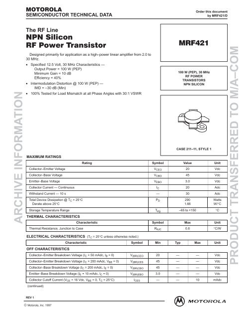
Motorola MRF421 transistor DataSheet (PDF) - EA1DDO
Motorola MRF421 transistor DataSheet (PDF) - EA1DDO
Motorola MRF421 transistor DataSheet (PDF) - EA1DDO

Create successful ePaper yourself
Turn your PDF publications into a flip-book with our unique Google optimized e-Paper software.
SEMICONDUCTOR TECHNICAL DATA<br />
Order this document<br />
by <strong>MRF421</strong>/D<br />
ARCHIVE INFORMATION<br />
The RF Line<br />
<br />
<br />
Designed primarily for application as a high–power linear amplifier from 2.0 to<br />
30 MHz.<br />
• Specified 12.5 Volt, 30 MHz Characteristics —<br />
Output Power = 100 W (PEP)<br />
Minimum Gain = 10 dB<br />
Efficiency = 40%<br />
• Intermodulation Distortion @ 100 W (PEP) —<br />
IMD = –30 dB (Min)<br />
• 100% Tested for Load Mismatch at all Phase Angles with 30:1 VSWR<br />
MAXIMUM RATINGS<br />
Rating Symbol Value Unit<br />
Collector–Emitter Voltage V CEO 20 Vdc<br />
Collector–Base Voltage V CBO 45 Vdc<br />
Emitter–Base Voltage V EBO 3.0 Vdc<br />
Collector Current — Continuous I C 20 Adc<br />
Withstand Current — 10 s — 30 Adc<br />
Total Device Dissipation @ T C = 25°C<br />
Derate above 25°C<br />
P D 290<br />
1.66<br />
Storage Temperature Range T stg –65 to +150 °C<br />
THERMAL CHARACTERISTICS<br />
Watts<br />
W/°C<br />
Characteristic Symbol Max Unit<br />
Thermal Resistance, Junction to Case R θJC 0.6 °C/W<br />
ELECTRICAL CHARACTERISTICS (T C = 25°C unless otherwise noted.)<br />
Characteristic Symbol Min Typ Max Unit<br />
OFF CHARACTERISTICS<br />
Collector–Emitter Breakdown Voltage (I C = 50 mAdc, I B = 0) V (BR)CEO 20 — — Vdc<br />
Collector–Emitter Breakdown Voltage (I C = 200 mAdc, V BE = 0) V (BR)CES 45 — — Vdc<br />
Collector–Base Breakdown Voltage (I C = 200 mAdc, I E = 0) V (BR)CBO 45 — — Vdc<br />
Emitter–Base Breakdown Voltage (I E = 10 mAdc, I C = 0) V (BR)EBO 3.0 — — Vdc<br />
Collector Cutoff Current (V CE = 16 Vdc, V BE = 0, T C = 25°C) I CES — — 10 mAdc<br />
(continued)<br />
<br />
100 W (PEP), 30 MHz<br />
RF POWER<br />
TRANSISTORS<br />
NPN SILICON<br />
CASE 211–11, STYLE 1<br />
PRODUCT TRANSFERRED TO M/A–COM<br />
REV 1<br />
© MOTOROLA RF DEVICE DATA<br />
<strong>Motorola</strong>, Inc. 1997<br />
<strong>MRF421</strong><br />
1
ELECTRICAL CHARACTERISTICS – continued (T C = 25°C unless otherwise noted.)<br />
Characteristic Symbol Min Typ Max Unit<br />
ON CHARACTERISTICS<br />
DC Current Gain<br />
(I C = 5.0 Adc, V CE = 5.0 Vdc)<br />
h FE 10 70 — —<br />
ARCHIVE INFORMATION<br />
DYNAMIC CHARACTERISTICS<br />
Output Capacitance<br />
(V CB = 12.5 Vdc, I E = 0, f = 1.0 MHz)<br />
FUNCTIONAL TESTS<br />
Common–Emitter Amplifier Power Gain<br />
(V CC = 12.5 Vdc, P out = 100 W, I C(max) = 10 Adc,<br />
I CQ = 150 mAdc, f = 30, 30.001 MHz)<br />
Collector Efficiency<br />
(V CC = 12.5 Vdc, P out = 100 W, I C(max) = 10 Adc,<br />
I CQ = 150 mA, f = 30, 30.001 MHz)<br />
Intermodulation Distortion (1)<br />
(V CE = 12.5 Vdc, P out = 100 W, I C = 10 Adc,<br />
I CQ = 150 mA, f = 30, 30.001 MHz)<br />
NOTE:<br />
1. To proposed EIA method of measurement. Reference peak envelope power.<br />
<br />
<br />
<br />
<br />
<br />
<br />
<br />
<br />
<br />
C1, C2, C4 — 170–780 pF, ARCO 469<br />
C3 — 80–480 pF, ARCO 466<br />
C5, C7, C10 — ERIE 0.1 µF, 100 V<br />
C6 — MALLORY 500 µF @ 15 V Electrolytic<br />
C9 — 100 µF, 15 V Electrolytic<br />
C8 — 1000 pF, 350 V UNDERWOOD<br />
R1 — 10 Ω, 25 Watt Wirewound<br />
<br />
<br />
<br />
<br />
<br />
Figure 1. 30 MHz Test Circuit Schematic<br />
C ob — 550 800 pF<br />
G PE 10 12 — dB<br />
η 40 — — %<br />
IMD — –33 –30 dB<br />
<br />
<br />
<br />
<br />
R2 — 10 Ω, 1.0 Watt Carbon<br />
CR1 — 1N4997<br />
L1 — 3 Turns, #16 Wire, 5/16″ I.D., 5/16″ Long<br />
L2 — 12 Turns, #16 Enameled Wire Closewound, 1/4″ I.D.<br />
L3 — 1–3/4 Turns, 1/8″ Tubing, 3/8″ I.D., 3/8″ Long<br />
L4 — 10 µH Molded Choke<br />
L5 — 10 Ferrite Beads — FERROXCUBE #56–590–65/3B<br />
<br />
<br />
<br />
<br />
<br />
<br />
<br />
<br />
<br />
PRODUCT TRANSFERRED TO M/A–COM<br />
<strong>MRF421</strong><br />
2<br />
MOTOROLA RF DEVICE DATA
ARCHIVE INFORMATION<br />
<br />
<br />
<br />
<br />
<br />
<br />
<br />
<br />
<br />
<br />
<br />
<br />
<br />
<br />
<br />
<br />
<br />
<br />
<br />
<br />
<br />
<br />
<br />
<br />
<br />
<br />
<br />
<br />
<br />
<br />
<br />
<br />
<br />
Figure 2. Output Power versus Input Power<br />
<br />
<br />
<br />
<br />
<br />
Figure 4. Power Gain versus Frequency<br />
°<br />
<br />
<br />
<br />
<br />
<br />
<br />
<br />
<br />
<br />
<br />
<br />
<br />
<br />
<br />
<br />
<br />
<br />
<br />
<br />
<br />
<br />
<br />
<br />
<br />
Figure 3. Output Power versus Supply Voltage<br />
<br />
<br />
<br />
<br />
<br />
<br />
<br />
<br />
Figure 5. Intermodulation Distortion<br />
versus Output Power<br />
<br />
<br />
<br />
<br />
<br />
<br />
<br />
<br />
<br />
<br />
<br />
<br />
<br />
<br />
<br />
<br />
<br />
<br />
<br />
<br />
PRODUCT TRANSFERRED TO M/A–COM<br />
Figure 6. DC Safe Operating Area<br />
Figure 7. Series Equivalent Impedance<br />
MOTOROLA RF DEVICE DATA<br />
<strong>MRF421</strong><br />
3
Figure 8. Output Capacitance versus Frequency<br />
Figure 9. Output Resistance versus Frequency<br />
PACKAGE DIMENSIONS<br />
A<br />
U<br />
M<br />
<br />
<br />
<br />
<br />
H<br />
J<br />
Q<br />
<br />
<br />
K<br />
<br />
<br />
D<br />
M<br />
E<br />
R<br />
C<br />
B<br />
<br />
<br />
<br />
<br />
<br />
<br />
<br />
<br />
<br />
<br />
<br />
<br />
<br />
<br />
<br />
<br />
<br />
<br />
<br />
<br />
<br />
<br />
CASE 211–11<br />
ISSUE N<br />
<strong>Motorola</strong> reserves the right to make changes without further notice to any products herein. <strong>Motorola</strong> makes no warranty, representation or guarantee regarding<br />
the suitability of its products for any particular purpose, nor does <strong>Motorola</strong> assume any liability arising out of the application or use of any product or circuit,<br />
and specifically disclaims any and all liability, including without limitation consequential or incidental damages. “Typical” parameters can and do vary in different<br />
applications. All operating parameters, including “Typicals” must be validated for each customer application by customer’s technical experts. <strong>Motorola</strong> does<br />
not convey any license under its patent rights nor the rights of others. <strong>Motorola</strong> products are not designed, intended, or authorized for use as components in<br />
systems intended for surgical implant into the body, or other applications intended to support or sustain life, or for any other application in which the failure of<br />
the <strong>Motorola</strong> product could create a situation where personal injury or death may occur. Should Buyer purchase or use <strong>Motorola</strong> products for any such<br />
unintended or unauthorized application, Buyer shall indemnify and hold <strong>Motorola</strong> and its officers, employees, subsidiaries, affiliates, and distributors harmless<br />
against all claims, costs, damages, and expenses, and reasonable attorney fees arising out of, directly or indirectly, any claim of personal injury or death<br />
associated with such unintended or unauthorized use, even if such claim alleges that <strong>Motorola</strong> was negligent regarding the design or manufacture of the part.<br />
<strong>Motorola</strong> and are registered trademarks of <strong>Motorola</strong>, Inc. <strong>Motorola</strong>, Inc. is an Equal Opportunity/Affirmative Action Employer.<br />
How to reach us:<br />
USA/EUROPE: <strong>Motorola</strong> Literature Distribution;<br />
JAPAN: Nippon <strong>Motorola</strong> Ltd.; Tatsumi–SPD–JLDC, Toshikatsu Otsuki,<br />
P.O. Box 20912; Phoenix, Arizona 85036. 1–800–441–2447 6F Seibu–Butsuryu–Center, 3–14–2 Tatsumi Koto–Ku, Tokyo 135, Japan. 03–3521–8315<br />
MFAX: RMFAX0@email.sps.mot.com – TOUCHTONE (602) 244–6609 HONG KONG: <strong>Motorola</strong> Semiconductors H.K. Ltd.; 8B Tai Ping Industrial Park,<br />
INTERNET: http://Design–NET.com 51 Ting Kok Road, Tai Po, N.T., Hong Kong. 852–26629298<br />
<strong>MRF421</strong><br />
4<br />
◊<br />
MOTOROLA RF DEVICE DATA <strong>MRF421</strong>/D