Hardware Design of Independent Experimental Platform ... - GSE
Hardware Design of Independent Experimental Platform ... - GSE
Hardware Design of Independent Experimental Platform ... - GSE

Create successful ePaper yourself
Turn your PDF publications into a flip-book with our unique Google optimized e-Paper software.
201O Second International Conference on Communication Systems, Networks and Applications<br />
<strong>Hardware</strong> <strong>Design</strong> <strong>of</strong> <strong>Independent</strong> <strong>Experimental</strong> <strong>Platform</strong> Based on FPGA<br />
HuHaoran<br />
Department <strong>of</strong> computer and<br />
information<br />
Anqing teaching college<br />
Anqing, China<br />
huhr@aqtc.edu.cn<br />
Wu Jiani<br />
USTC-CityU Joint Advanced<br />
Research Center<br />
USTC<br />
Suzhou, China<br />
wujiani@mail.ustc.edu.cn<br />
Zhang Fei<br />
Department <strong>of</strong> computer and<br />
information<br />
Anqing teaching college<br />
Anqing, China<br />
zhangf@163.com<br />
Abstract-This article introduced the EDA technology<br />
development course, and has made certain description on its<br />
basic characteristic and the development process. Meanwhile<br />
this article has made the detailed introduction to the<br />
programmable logical component's present situation and the<br />
unique feature. It emphatically elaborated the present<br />
popular FPGA technology. This article aims at designing an<br />
independent experimental platform based on the present<br />
popular FPGA component. The hardware part takes<br />
ALTERA Corporation's CYCLONE series chips as the core,<br />
including LED array, seven digital tube display, cluster<br />
communication, key-stroke input and so on. At last,we carry<br />
out the confirmation <strong>of</strong> the experiment platform through<br />
some simple VHDL programs.<br />
Keywords-<strong>Independent</strong> <strong>Experimental</strong> <strong>Platform</strong>; FPGA;<br />
EDA technology<br />
I. INTRODUCTION<br />
Throughout the history <strong>of</strong> EDA technology, EDA<br />
technology has undergone three continuous stages. Namely,<br />
CAD (computer-aided design) phase, EDA (electronic<br />
design automation) phase and ESDA (Electronic Systems<br />
<strong>Design</strong> Automation) phase.<br />
The 20th century, 80 years, with the growing size <strong>of</strong><br />
electronic products, systems are more complex, as well as<br />
semiconductor fabrication/production technology<br />
continues to improve, the original CAD technology has<br />
been unable to meet high-capacity chips and highfrequency,<br />
large-scale circuits design requirements, it is<br />
hoped to have a successful experience with mature<br />
technology and to complete electronic product<br />
development approach, the question arose EDA<br />
technology. Second-generation EDA tools, s<strong>of</strong>tware<br />
applications are mainly digital circuit analysis, analog<br />
circuit analysis, printed circuit boards, field programmable<br />
gate array place and route functions.<br />
The 20th century, the late 90s, the major EDA vendors<br />
began to launch a high-level language description, systemlevel<br />
simulation and synthesis technology as the core <strong>of</strong><br />
the third-generation EDA tools. Third-generation EDA<br />
tools for logic synthesis, hardware behavior simulation,<br />
parametric analysis and testing focused on providing a<br />
complete range <strong>of</strong> system design and to meet the needs <strong>of</strong><br />
all the development tools, for example, describe the design<br />
intent <strong>of</strong> the design entry tool with logic synthesis and<br />
design optimization capabilities design tools, as well as the<br />
solemn performance <strong>of</strong> the design and evaluation <strong>of</strong><br />
simulation tools [1].<br />
II.<br />
STRUCTURE AND APPLICATION OF FPGA<br />
With the development <strong>of</strong> micro-electronics design<br />
technology, and digital integrated circuits gradually<br />
developed into today's application specific integrated<br />
circuit (ASIC) from the tubes, transistors, small and<br />
medium-scale integrated circuits, ultra-large scale<br />
integrated circuit (VLSIC). The emergence <strong>of</strong> ASIC<br />
reduces production costs, and improves system reliability,<br />
reduces the physical size <strong>of</strong> the design and promotes the<br />
process <strong>of</strong> digitalization <strong>of</strong> society. But the long design<br />
cycle <strong>of</strong> ASIC, revision and massive investments and poor<br />
flexibility restricts its wider application. <strong>Hardware</strong><br />
engineers hope to have a more flexible design approach, if<br />
necessary, large-scale digital logic could be designed and<br />
changed in the laboratory, and to develop its own ASIC<br />
and inunediately put into use, it is the basic idea <strong>of</strong><br />
programmable logic devices.<br />
Programmable logic devices with the development <strong>of</strong><br />
microelectronics manufacturing process have made<br />
considerable progress. From<br />
the simple logic functions<br />
programmable read-only memory, UV-erasable read-only<br />
memory and electrically erasable read-only memory<br />
(E2PROM) to programmable array logic (PLA) and<br />
generic array logic (GAL), now we can complete today a<br />
complex combination <strong>of</strong> ultra-large-scale logic and timing<br />
complex programmable logic device (CPLD ) and fieldprogrammable<br />
logic devices (FPGA). As the process<br />
technology development and market needs, a new<br />
FPGAlCPLD with ultra-large-scale, high-speed, low<br />
power consumption has appeared. The new generation <strong>of</strong><br />
FPGA even integrates the central processing unit (CPU) or<br />
digital processor (DSP) cores, can do the hardware and<br />
s<strong>of</strong>tware co-design in an FPGA and provides a Powerful<br />
hardware support[3] for the realization <strong>of</strong> on-chip<br />
programmable system.<br />
III.<br />
FPGA HARDWARE DESIGN OF EXPERIMENT<br />
PLATFORM<br />
A. FPGA in Hurricane Series <strong>of</strong> Altera<br />
There are at present more than a dozen productions <strong>of</strong><br />
CPLDIFPGA companies, a higher market share is three<br />
Altera, Xilinx, and Lattice Corporation. Which, Altera and<br />
Xilinx have more than 60% market share. Most <strong>of</strong> the<br />
above companies have their own different FPGA product<br />
family, such as Lattice's EC / ECP series <strong>of</strong> devices,<br />
Altera's Apex, Cyclone, Stratix series devices, as well as<br />
Xilinx's Spartan and Virtex series <strong>of</strong> devices. The<br />
company's product mix is different design methods and<br />
978-1-4244-7477-6/10/$26.00 ©2010 IEEE<br />
ICCSNA2010<br />
44
scope <strong>of</strong> application is also different. In the comprehensive<br />
comparison <strong>of</strong> various vendor devices, development<br />
s<strong>of</strong>tware, market conditions, based on the paper selected a<br />
price higher than the general chip market applications, that<br />
Altera's Cyclone series <strong>of</strong> EPIC3T144C8, as an<br />
experiment to study the main chip board. The logic unit is<br />
2910, 13 internal RAM modules, the maximum available<br />
110 port 104. The chip's versatile strong, affordable,<br />
develop a more suitable learning environment s<strong>of</strong>tware<br />
platform. FPGA configuration chip EPCS 1, single-chip<br />
capacity <strong>of</strong> 1M bits, can be powered down to save the data.<br />
Download circuit with JT AG and AS modes <strong>of</strong> two to<br />
download in order to achieve online and download the<br />
debugging [7]. S<strong>of</strong>tware platform uses Altera's Quartus II<br />
development environment. Cyclone series FPGA structure<br />
as shown in Figure 1.<br />
We designed 3.3V and 1.5V DC power supply. The<br />
circuit schematic diagram is shown in Figure 3 and Figure<br />
4.<br />
1 -::+e5<br />
vees<br />
--<br />
Lf<br />
---.L<br />
-=-<br />
3<br />
UI 1085<br />
IN<br />
ADJ!GND<br />
I<br />
I<br />
Figure 3.<br />
alIT<br />
2<br />
VCC3.3<br />
--<br />
+<br />
<br />
-=-<br />
-'-<br />
RI<br />
R2<br />
C9<br />
3.3V Power Supply<br />
vecs 112 1085<br />
,--__ ---, VCC1.S<br />
C2<br />
VCCIO<br />
VCCIO<br />
.---J.IN ADJ/GND alIT I--+---"-<br />
rl--+---
and will receive the down by the MODEM carrier signal<br />
demodulation into a digital data, sent along the receive<br />
data line RXD terminal.<br />
RI-Ring Indicator, when the MODEM receive the<br />
switch signals sent by ringing call to be effective to notify<br />
the terminal had to be called.<br />
TXD-transmit data through the serial data TXD data<br />
lines will be sent to the MODEM, DTE -> DCE.<br />
RXD-receive data received through the RXD data line<br />
sent from the MODEM serial data, DCE -> DTE.<br />
basic structure <strong>of</strong> Simple programmable logic device is<br />
shown in Figure 6.<br />
XI --.---------I<br />
Xn --..-----1<br />
PI<br />
Pd<br />
----1---Z1<br />
« or<br />
" array<br />
TABLE I.<br />
RS232 PIN ASSIGNMENT INSTRUCTIONS<br />
L-____ ------_Zm<br />
DSR<br />
Pin Shorthand Significance<br />
Pin 1 DCD carrier detect<br />
Pin2 RXD receive<br />
Pin3 TXD transmit<br />
Pin4 DTR data terminal ready<br />
Pin5 GND ground<br />
Pin6 DSR data set ready<br />
Pin7 RTS request to send<br />
Pin8 CTS clear to send<br />
Pin9 RI ring indicator<br />
9-pin RS232 interface pins are shown in Figure 5.<br />
RTS 0<br />
CTS<br />
Rl<br />
DCD<br />
RXD<br />
TXD<br />
DTR<br />
GND<br />
Figure 6. The Basic Structure <strong>of</strong> Programmable Logic Devices<br />
From the figure we can see, assuming that<br />
programmable logic device input number n, the output<br />
number m, the number <strong>of</strong> the product items d, Then the<br />
device chip area can be expressed as: S = (2n + m) * d.<br />
For "and/or" array, the designer can change specific<br />
connections <strong>of</strong> "and/or" array to achieve a different logic<br />
functions. Usually, as long as any <strong>of</strong> an array <strong>of</strong><br />
connection <strong>of</strong> "and/or" array changes, then the<br />
corresponding programmable logic device functions will<br />
change. In the digital circuit, according to different<br />
combinations form <strong>of</strong> "and/or" array in programmable<br />
logic devices, a simple programmable logic device is<br />
divided into three types: (1) Programmable read-only<br />
memory (PROM), which is characterized with fixed "and"<br />
array and programmable "or"array; (2) The programmable<br />
logic array (PLA), which is characterized with<br />
programmable "and/or" array; (3) Programmable array<br />
logic (PAL), which is characterized with fixed "or" array<br />
and programmable "and"array.<br />
V. PROGRAM SAMPLE OF EXPERIMENTAL PLATFORM<br />
Figure 5. RS232 Interface Pin Map<br />
As the RS232 electrical characteristics and FPGA are<br />
different, so the middle to connect an interface chip to<br />
complete the RS232 negative TTL logic and FPGA-level<br />
conversion between.<br />
IV. BASIC STRUCTURE AND CHARACTERISTICS OF PLD<br />
Programmable logic device is a new integrated device<br />
developed from the 20th century, 70 years, the user can<br />
achieve the required logic functions through programming<br />
for the device, programmable logic device is a semicustom<br />
integrated circuits. Because PLD is <strong>of</strong> relatively<br />
low cost, flexibility, short design cycle, and high reliability,<br />
risk, thus has been widely applied, and develop very<br />
rapidly [4].<br />
PLD can be divided into simple PLD, EPLD/CPLD,<br />
FPGA. Simple PLD including PROM, PLA, PAL and<br />
GAL, is characterized by the composition "and" array and<br />
"or" array, which can effectively achieve the logic<br />
functions with "addition <strong>of</strong> product" form. According to<br />
Boolean algebra knowledge, all <strong>of</strong> the logic functions may<br />
be described using "and/or" expression, so by changing the<br />
connection <strong>of</strong> "or" array and "and" array we can<br />
implement different logic functions, a simple combination<br />
<strong>of</strong> PLD is mainly used to achieve the logic function. The<br />
Experiment content define an input clock port "clkin",<br />
an clock output port "clkout" and 7 keyboard input ports<br />
"sound (0-7)", input clock frequency <strong>of</strong> I.SM, each key<br />
pressed corresponds to a sound state ,can input clock<br />
frequency <strong>of</strong> sub-frequency <strong>of</strong> the corresponding seven<br />
different frequencies.<br />
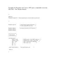
Example procedures are as follows:<br />
library ieee;<br />
use ieee.std _logic _1164.all;<br />
use ieee.std _logic _ unsigned. all;<br />
entity fs is<br />
porte elkin: in std _logic;<br />
sound: in std_logic_vector(7 downto 1);<br />
elkoutout std_logic);<br />
end fs;<br />
architecture behave <strong>of</strong> fs is<br />
begin<br />
process( elkin)<br />
variable count integer range 0 to 3000;<br />
begin<br />
if (clkin'event and clkin='I') then<br />
case sound is<br />
when "1111110"=><br />
case count is<br />
when 0 to 1433=><br />
46
clkout<br />
clkout<br />
clkoutcount:=O;<br />
end case;<br />
when" 1111101"=><br />
case count is<br />
when 0 to 1278=><br />
clkout<br />
clkout<br />
clkoutcount:=O;<br />
end case;<br />
when "1111011"=><br />
case count is<br />
when 0 to 1137=><br />
clkout<br />
clkout<br />
clkoutcount:=O;<br />
end case;<br />
when" 1110111"=><br />
case count is<br />
when 0 to 1074=><br />
clkout<br />
clkout<br />
clkoutcount:=O;<br />
end case;<br />
when"IIOIIII"=><br />
case count is<br />
when 0 to 955=><br />
clkout<br />
clkout <br />
clkoutcount:=O;<br />
end case;<br />
when "1011111"=><br />
case count is<br />
when 0 to 851=><br />
clkout<br />
clkout<br />
clkoutcount:=O;<br />
end case;<br />
when "0111111"=><br />
case count is<br />
when 0 to 758=><br />
clkout<br />
clkout<br />
clkoutcount:=O;<br />
end case;<br />
when others=><br />
clkout