BPW21R Silicon PN Photodiode
BPW21R Silicon PN Photodiode
BPW21R Silicon PN Photodiode

Create successful ePaper yourself
Turn your PDF publications into a flip-book with our unique Google optimized e-Paper software.
<strong>Silicon</strong> <strong>PN</strong> <strong>Photodiode</strong><br />
Description<br />
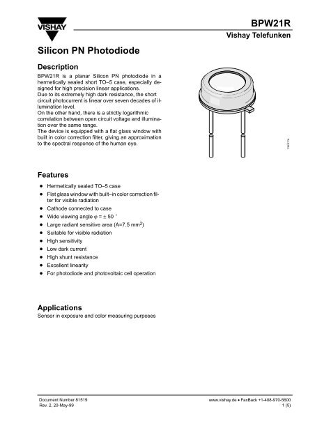
<strong>BPW21R</strong> is a planar <strong>Silicon</strong> <strong>PN</strong> photodiode in a<br />
hermetically sealed short TO–5 case, especially designed<br />
for high precision linear applications.<br />
Due to its extremely high dark resistance, the short<br />
circuit photocurrent is linear over seven decades of illumination<br />
level.<br />
On the other hand, there is a strictly logarithmic<br />
correlation between open circuit voltage and illumination<br />
over the same range.<br />
The device is equipped with a flat glass window with<br />
built in color correction filter, giving an approximation<br />
to the spectral response of the human eye.<br />
<strong>BPW21R</strong><br />
Vishay Telefunken<br />
94 8394<br />
Features<br />
<br />
<br />
Hermetically sealed TO–5 case<br />
Flat glass window with built–in color correction filter<br />
for visible radiation<br />
Cathode connected to case<br />
Wide viewing angle ϕ = ± 50 <br />
Large radiant sensitive area (A=7.5 mm 2 )<br />
Suitable for visible radiation<br />
High sensitivity<br />
Low dark current<br />
High shunt resistance<br />
Excellent linearity<br />
For photodiode and photovoltaic cell operation<br />
Applications<br />
Sensor in exposure and color measuring purposes<br />
Document Number 81519<br />
Rev. 2, 20-May-99<br />
www.vishay.de • FaxBack +1-408-970-5600<br />
1 (5)
<strong>BPW21R</strong><br />
Vishay Telefunken<br />
Absolute Maximum Ratings<br />
T amb = 25 C<br />
Parameter Test Conditions Symbol Value Unit<br />
Reverse Voltage V R 10 V<br />
Power Dissipation T amb 50 C P V 300 mW<br />
Junction Temperature T j 125 C<br />
Operating Temperature Range T amb –55...+125 C<br />
Storage Temperature Range T stg –55...+125 C<br />
Soldering Temperature t 5 s T sd 260 C<br />
Thermal Resistance Junction/Ambient R thJA 250 K/W<br />
Basic Characteristics<br />
T amb = 25 C<br />
Parameter Test Conditions Symbol Min Typ Max Unit<br />
Forward Voltage I F = 50 mA V F 1.0 1.3 V<br />
Breakdown Voltage I R = 20 A, E = 0 V (BR) 10 V<br />
Reverse Dark Current V R = 5 V, E = 0 I ro 2 30 nA<br />
Diode Capacitance V R = 0 V, f = 1 MHz, E = 0 C D 1.2 nF<br />
V R = 5 V, f = 1 MHz, E = 0 C D 400 pF<br />
Dark Resistance V R = 10 mV R D 38 G<br />
Open Circuit Voltage E A = 1 klx V o 280 450 mV<br />
Temp. Coefficient of V o E A = 1 klx TK Vo –2 mV/K<br />
Short Circuit Current E A = 1 klx I k 4.5 9 A<br />
Temp. Coefficient of I k E A = 1 klx TK lk –0.05 %/K<br />
Reverse Light Current E A = 1 klx, V R = 5 V I ra 4.5 9 A<br />
Sensitivity V R = 5 V, E A = 10 –2 ...10 5 lx S 9 nA/lx<br />
Angle of Half Sensitivity ϕ ±50 deg<br />
Wavelength of Peak Sensitivity p 565 nm<br />
Range of Spectral Bandwidth 0.5 420...675 nm<br />
Rise Time V R = 0 V, R L = 1k ,<br />
t r 3.1 s<br />
= 660 nm<br />
Fall Time V R = 0 V, R L = 1k ,<br />
= 660 nm<br />
t f 3.0 s<br />
www.vishay.de • FaxBack +1-408-970-5600 Document Number 81519<br />
2 (5) Rev. 2, 20-May-99
Typical Characteristics (T amb = 25 C unless otherwise specified)<br />
<strong>BPW21R</strong><br />
Vishay Telefunken<br />
I ro – Reverse Dark Current ( nA )<br />
10 4 V R =5V<br />
1400<br />
10 3<br />
10 2<br />
10 1<br />
C D – Diode Capacitance ( pF )<br />
1200<br />
1000<br />
800<br />
600<br />
400<br />
200<br />
E=0<br />
f=1MHz<br />
10 0<br />
20<br />
40 60 80 100 120<br />
0<br />
0.1 1 10<br />
100<br />
94 8468<br />
T amb – Ambient Temperature ( °C )<br />
94 8473<br />
V R – Reverse Voltage ( V )<br />
Figure 1. Reverse Dark Current vs. Ambient Temperature<br />
Figure 4. Diode Capacitance vs. Reverse Voltage<br />
I ra rel – Relative Reverse Light Current<br />
94 8738<br />
1.3<br />
1.2<br />
1.1<br />
1.0<br />
0.9<br />
0.8<br />
0 20 40 60 80<br />
100<br />
T amb – Ambient Temperature ( °C )<br />
120<br />
S ( ) rel – Relative Spectral Sensitivity<br />
1.0<br />
0.8<br />
0.6<br />
0.4<br />
0.2<br />
V Eye<br />
94 8477<br />
0<br />
350 450 550 650<br />
– Wavelength ( nm )<br />
750<br />
Figure 2. Relative Reverse Light Current vs.<br />
Ambient Temperature<br />
10 2<br />
Figure 5. Relative Spectral Sensitivity vs. Wavelength<br />
0°<br />
10<br />
°<br />
20<br />
°<br />
30°<br />
I – Short Circuit Current ( A )<br />
k<br />
10 1<br />
10 0<br />
10 –1<br />
10 –2<br />
10 –3<br />
10 –4<br />
10 –2 10 –1 10 0 10 1 10 2 10 3 10 4<br />
S rel – Relative Sensitivity<br />
1.0<br />
0.9<br />
0.8<br />
0.7<br />
0.6<br />
0.4 0.2 0 0.2 0.4<br />
40°<br />
50°<br />
60°<br />
70°<br />
80°<br />
0.6<br />
94 8476<br />
E A – Illuminance ( lx )<br />
94 8475<br />
Figure 3. Short Circuit Current vs. Illuminance<br />
Figure 6. Relative Radiant Sensitivity vs.<br />
Angular Displacement<br />
Document Number 81519<br />
Rev. 2, 20-May-99<br />
www.vishay.de • FaxBack +1-408-970-5600<br />
3 (5)
<strong>BPW21R</strong><br />
Vishay Telefunken<br />
Dimensions in mm<br />
96 12181<br />
www.vishay.de • FaxBack +1-408-970-5600 Document Number 81519<br />
4 (5) Rev. 2, 20-May-99
<strong>BPW21R</strong><br />
Vishay Telefunken<br />
Ozone Depleting Substances Policy Statement<br />
It is the policy of Vishay Semiconductor GmbH to<br />
1. Meet all present and future national and international statutory requirements.<br />
2. Regularly and continuously improve the performance of our products, processes, distribution and operating<br />
systems with respect to their impact on the health and safety of our employees and the public, as well as their<br />
impact on the environment.<br />
It is particular concern to control or eliminate releases of those substances into the atmosphere which are known as<br />
ozone depleting substances (ODSs).<br />
The Montreal Protocol (1987) and its London Amendments (1990) intend to severely restrict the use of ODSs and<br />
forbid their use within the next ten years. Various national and international initiatives are pressing for an earlier ban<br />
on these substances.<br />
Vishay Semiconductor GmbH has been able to use its policy of continuous improvements to eliminate the use of<br />
ODSs listed in the following documents.<br />
1. Annex A, B and list of transitional substances of the Montreal Protocol and the London Amendments respectively<br />
2. Class I and II ozone depleting substances in the Clean Air Act Amendments of 1990 by the Environmental<br />
Protection Agency (EPA) in the USA<br />
3. Council Decision 88/540/EEC and 91/690/EEC Annex A, B and C (transitional substances) respectively.<br />
Vishay Semiconductor GmbH can certify that our semiconductors are not manufactured with ozone depleting<br />
substances and do not contain such substances.<br />
We reserve the right to make changes to improve technical design and may do so without further notice.<br />
Parameters can vary in different applications. All operating parameters must be validated for each customer application<br />
by the customer. Should the buyer use Vishay-Telefunken products for any unintended or unauthorized application, the<br />
buyer shall indemnify Vishay-Telefunken against all claims, costs, damages, and expenses, arising out of, directly or<br />
indirectly, any claim of personal damage, injury or death associated with such unintended or unauthorized use.<br />
Vishay Semiconductor GmbH, P.O.B. 3535, D-74025 Heilbronn, Germany<br />
Telephone: 49 (0)7131 67 2831, Fax number: 49 (0)7131 67 2423<br />
Document Number 81519<br />
Rev. 2, 20-May-99<br />
www.vishay.de • FaxBack +1-408-970-5600<br />
5 (5)