easyScan 2 brochure (1.1 MB) - Schaefer Technology
easyScan 2 brochure (1.1 MB) - Schaefer Technology
easyScan 2 brochure (1.1 MB) - Schaefer Technology

Create successful ePaper yourself
Turn your PDF publications into a flip-book with our unique Google optimized e-Paper software.
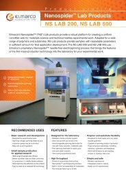
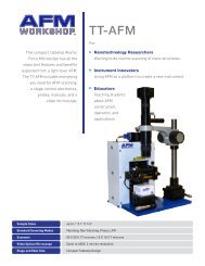
Basic STM Package<br />
The first scanning tunneling microscope (STM) was developed by Gerd Binnig and Heinrich Rohrer from the IBM research<br />
laboratory in Rüschlikon, Switzerland, and first made atoms accessible to trained scientists. The <strong>easyScan</strong> 2 STM goes a step<br />
further and makes atoms accessible for everyone.<br />
This is why, around the globe, hundreds of <strong>easyScan</strong> STMs form a crucial part of nanoeducation, whether in the framework<br />
of physics, chemistry, or materials science. Teachers appreciate the easy and hassle-free classroom demonstrations they can<br />
offer, and students find themselves motivated by the rapid success of their first step into practical nanoscience, be it in a lab<br />
assignment or a research project, in high school or graduate studies. Tips for the STM are simply cut from a Pt/Ir wire without<br />
any etching in hazardous substances, and the <strong>easyScan</strong> system’s low voltage further ensures the operator’s safety.<br />
The <strong>easyScan</strong> STM has also established itself as a full-fledged research and development tool. Applications range from routine<br />
process control such as spot-checking nanocircuitry to fundamental research such as single electron spin detection and<br />
spectroscopy. Now, with the <strong>easyScan</strong> 2 series and its Signal Module, scientists can expand the possibilities of their <strong>easyScan</strong><br />
STM even further. And, thanks to its ease of use, those who want to use their STM for student labs can, without fearing damage<br />
to their research equipment.<br />
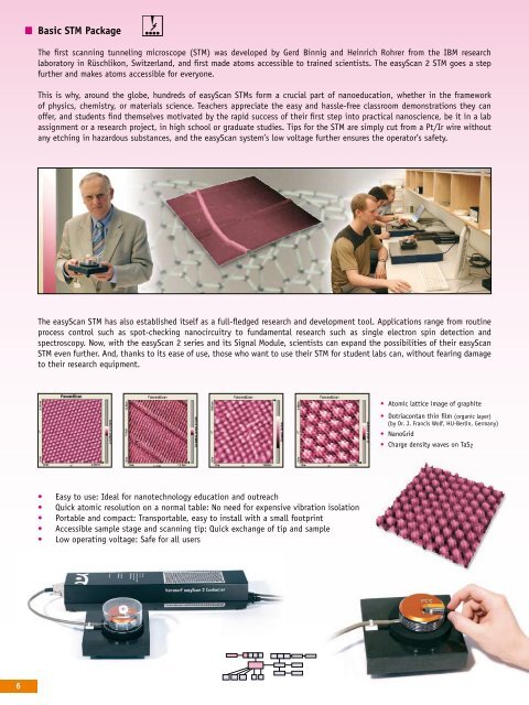
• Atomic lattice image of graphite<br />
• Dotriacontan thin film (organic layer)<br />
(by Dr. J. Francis Wolf, HU-Berlin, Germany)<br />
• NanoGrid<br />
• Charge density waves on TaS 2<br />
• Easy to use: Ideal for nanotechnology education and outreach<br />
• Quick atomic resolution on a normal table: No need for expensive vibration isolation<br />
• Portable and compact: Transportable, easy to install with a small footprint<br />
• Accessible sample stage and scanning tip: Quick exchange of tip and sample<br />
• Low operating voltage: Safe for all users<br />
6