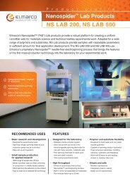
MikroMasch Brochure (1.8 MB) - Schaefer Technology
MikroMasch Brochure (1.8 MB) - Schaefer Technology
MikroMasch Brochure (1.8 MB) - Schaefer Technology
- No tags were found...

You also want an ePaper? Increase the reach of your titles
YUMPU automatically turns print PDFs into web optimized ePapers that Google loves.
<strong>MikroMasch</strong>®SPM Probes & Test Structureswww.spmtips.com<strong>MikroMasch</strong>® HeadquartersInnovative Solutions Bulgaria Ltd.48 Joliot Curie St.1113 Sofia, Bulgariaphone: +359 2 865-8629fax: +359 2 963-0732info@mikromasch.comsales@mikromasch.com<strong>MikroMasch</strong>® EuropeNanoAndMore GmbHSpilburg Bld. A1,Steinbühlstrasse 7D-35578 Wetzlar, GermanyToll Free (EU): +8000 SPMTIPS (776-8477)phone: + 49 6441-870-6272fax: + 49 6441-870-6274europe@mikromasch.com<strong>MikroMasch</strong>® USANanoAndMore USA Corp.9 James F. Byrnes StreetLady’s Island, SC 29907, USAToll Free (US): +1 866 SPMTIPS (776-8477)phone: +1 843-521-1108fax: +1 843-521-1148usa@mikromasch.com<strong>MikroMasch</strong>® Distributor<strong>MikroMasch</strong> ® is a trademark of NanoWorld AG operated by ISB Ltd.
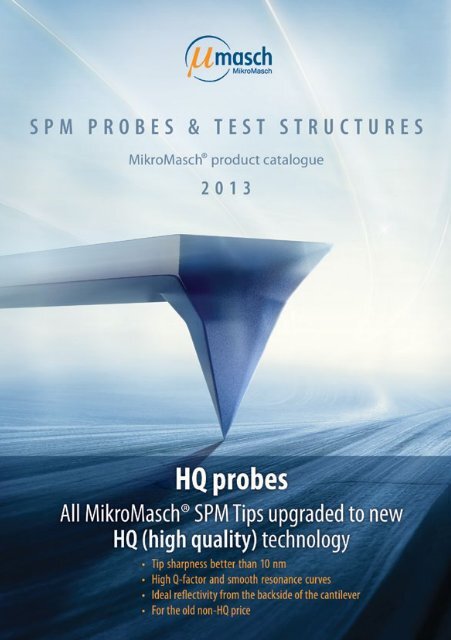
newall spm tips Improved To HQImproved HQ ProbesAll <strong>MikroMasch</strong> probes have been upgraded to an improved design, called the HQ Line (High Quality Line).“HQ” is a new series of probes distinguished by their high quality and high repeatability of characteristics, available due to a brandnew manufacturing process. In particular, the probes have much more consistent reflectivity from uncoated cantilevers, tip radiusand quality factor compared to our former non-HQ probes. The chips also have cut corners that allow them to be used at an anglefrom the vertical.Nominal characteristics of the premium quality probes are kept close to the former non-HQ <strong>MikroMasch</strong> product line. Describedbelow are some of the main advantages of the improved HQ Probes.Radius of Curvature< 7 nm1%94%The radius of curvature measures the sharpness of a particularprobe. Typically, the sharper the curvature radius the morefragile a silicon tip is. Conversely, a larger curvature radiusprovides greater durability, but reduces the benefits of asharper tip.Achieving a consistent balance delivers reliable and accurateresults. 94% of HQ probes have a radius of curvature between7 and 10 nm.7 to 10 nm> 10 nm 5%*for all standard, uncoated tips< 1.42%92%TIP SHAPE FACTORA higher value indicates a higher aspect ratio probe. A tighterrange of values indicates a more consistent tip shape.Results of the tip shape factor tests show consistent and closegrouping of data. Known tip shape insures accuracy of results.92% of HQ probes have an aspect ratio between 1.4 and <strong>1.8</strong>.1.4 to <strong>1.8</strong>> <strong>1.8</strong>6%*for all standard, uncoated tips< 320 kHz2%93%RESONANCE FREQUENCYProbes are designed to maintain a tight range of resonancefrequencies. Reliability in cantilever specifications ensuresdependable measurement results.320 to 380 kHz380 to 400 kHz5%*NSC15 Probes
contentThe New HQ Line & Test StructuresProbe chip specifications . . . . . . . . . . . . . . . . . . . . . . . . . 5regularNoncontact and Contact silicon probes . . . . . . . . . . . . . . . . 6TiplessNoncontact and Contact Tipless silicon probes . . . . . . . . . . . . 8Long Scanning / lifetimeHardened DLC coated silicon probes . . . . . . . . . . . . . . . . . . 9ConductiveDPER: High Resolution Conductive silicon probes. . . . . . . . . . 10DPE: Low Noise Conductive silicon probes . . . . . . . . . . . . . . 11Conductive Noncontact and Contact silicon probes . . . . . . . . 12MagneticMagnetic Noncontact silicon probes . . . . . . . . . . . . . . . . . 14High ResolutionHi’Res-C: High Resolution silicon probes . . . . . . . . . . . . . . . 15test structuresTGXYZ Series Calibration standards . . . . . . . . . . . . . . . . . . 16TGX Series Calibration standards . . . . . . . . . . . . . . . . . . . 16PA Series Calibration standards . . . . . . . . . . . . . . . . . . . . 17HOPG. . . . . . . . . . . . . . . . . . . . . . . . . . . . . . . . . . . . 17recomendationsRecommendations for specific applications . . . . . . . . . . . . . 18
Probe chip specificationsHQ:NSC/CSC 1-leverHQ: 4-leverCantilever material . . . . . . . . . . . . . . . n-type siliconTip shape . . . . . . . . . . . . . . . . . . . . . . . . pyramidalTip height . . . . . . . . . . . . . . . . . . . . . . . 12 - 18 µmCantilever material . . . . . . . . . . . . . . . n-type siliconTip shape . . . . . . . . . . . . . . . . . . . . . . . .pyramidalTip height . . . . . . . . . . . . . . . . . . . . . . . 12 - 18 µmSeries: 14, 15, 16, 17, 18, 19Series: XSC11HQ:NSC 3-leverHQ: NSC Tipless 3-leverCantilever material . . . . . . . . . . . . . . . n-type siliconTip shape . . . . . . . . . . . . . . . . . . . . . . . . pyramidalTip height . . . . . . . . . . . . . . . . . . . . . . . 12 - 18 µmSeries: 35, 36Cantilever material . . . . . . . . . . . . . . . n-type siliconSeries: 35,36 TiplessHQ:CSC 3-leverCantilever material . . . . . . . . . . . . . . . n-type siliconTip shape . . . . . . . . . . . . . . . . . . . . . . . . pyramidalTip height . . . . . . . . . . . . . . . . . . . . . . . 12 - 18 µmSeries: 37, 38HQ: CSC Tipless 3-leverCantilever material . . . . . . . . . . . . . . . n-type siliconSeries: 37, 38 Tipless5
egularHQ: NSC, CSC & XSCNoncontact (NSC), Contact (CSC) and 4-Lever (XSC) silicon probesPyramidal silicon etched probes* are characterized by high tip sharpness and narrow resonancepeaks, making them very suitable for topography imaging in dynamic AFM modes andcompositional mapping. These probes are available in a wide range of resonance frequenciesand spring constants.100 nmSEM image of the regularsilicon tipTip properties:Tip radius . . . . . . . . . . . . . . . . . ~ 8 nmTip material. . . . . . . . . . . . . . . . . siliconBackside coating:Al BS. . . . . . . . . . . . . . . . . . . Al 30 nmno Al . . . . . . . . . . . . . . . . . . . . . . noneCr-Au BS . . Au 30 nm on Cr 20 nm sublayerCantileverSeriesAvailableCoatingsLengthl, ± 5 µmWidthw, ± 3 µmThickness± 0.5 µmResonance FrequencykHz(typical) (range)Force ConstantN/m(typical) (range)HQ:NSC14HQ:NSC15HQ:NSC16HQ:CSC17HQ:NSC18HQ:NSC19/No Al, /Al BS/No Al, /Al BS, /Cr-Au BS/No Al, /Al BS/No Al, /Al BS/No Al, /Al BS, /Cr-Au BS/No Al, /Al BS125125225450225125253037.55027.522.52.14.07.02.03.01.0160325190137565110 - 220265 - 410170 - 21010 - 1760 - 9025 - 1205.040450.182.80.5<strong>1.8</strong> - 1320 - 8030 - 700.06 - 0.401.2 - 5.50.05 - 2.3HQ:NSC35lever Alever B/No Al, /Al BS, /Cr-Au BS1109035352.02.0205300130 - 290185 - 4308.9162.7 - 244.8 - 44lever C130352.015095 - 2055.41.7 - 14HQ:NSC36lever Alever B/No Al, /Al BS, /Cr-Au BS1109032.532.51.01.09013030 - 16045 - 2401.020.1 - 4.60.2 - 9lever C13032.51.06525 - 1150.60.06 - 2.7HQ:CSC37lever Alever B/No Al, /Al BS25035035352.02.0402030 - 5515 - 300.80.30.3 - 20.1 - 0.6lever C300352.03020 - 400.40.1 - 1HQ:CSC38lever Alever B/No Al, /Al BS25035032.532.51.01.020108 - 325 - 170.090.030.01 - 0.360.003 - 0.13lever C30032.51.0146 - 230.050.005 - 0.21HQ:XSC11lever A500302.71512 - 180.20.1 - 0.4lever Blever C/No Al, /Al BS21015030302.72.78015560 - 100115 - 2002.771.1 - 5.63 - 16lever D100502.7350250 - 4654217 - 906* See specifications on page 5
conductivePt and Cr-Au CoatedConductive Noncontact (NSC), Contact (CSC) and 4-Lever (XSC) silicon probesPyramidal silicon etched probes* with conductive platinum or gold coatings are suitable for awide range of electrical applications of AFM. Gold and platinum coatings are inert, which makesthese probes applicable for many experiments in biology and chemistry.100 nmSEM image of the conductingsilicon tipPt coated resulting tip radius . . . . < 30 nmPt overall coating. . . . . . . . . . . . . 30 nmCr-Au coated resulting tip radius < 35 nmAu overall coating . . . . . . . . . . . . 30 nmCr overall sublayer . . . . . . . . . . . . 20 nmCantileverSeriesAvailableCoatingsLengthl, ± 5 µmWidthw, ± 3 µmThickness± 0.5 µmResonance FrequencykHz(typical) (range)Force ConstantN/m(typical) (range)HQ:NSC14/Cr-Au, /Pt125252.1160110 - 2205.0<strong>1.8</strong> - 13HQ:NSC15/Cr-Au, /Pt125304.0325265 - 4104020 - 80HQ:NSC16/Cr-Au,22537.57.0190170 - 2104530 - 70HQ:CSC17/Cr-Au, /Pt450502.01310 - 170.180.06 - 0.40HQ:NSC18/Cr-Au, /Pt22527.53.07560 - 902.81.2 - 5.5HQ:NSC19/Cr-Au12522.51.06525 - 1200.50.05 - 2.3HQ:NSC35lever A110352.0205130 - 2908.92.7 - 24lever B/Cr-Au, /Pt90352.0300185 - 430164.8 - 44lever C130352.015095 - 2055.41.7 - 14HQ:NSC36lever A11032.51.09030 - 1601.00.1 - 4.6lever B/Cr-Au, /Pt9032.51.013045 - 24020.2 - 9lever C13032.51.06525 - 1150.60.06 - 2.7HQ:CSC37lever A250352.04030 - 550.80.3 - 2lever B/Cr-Au, /Pt350352.02015 - 300.30.1 - 0.6lever C300352.03020 - 400.40.1 - 1HQ:CSC38lever A25032.51.0208 - 320.090.01 - 0.36lever B/Cr-Au35032.51.0105 - 170.030.003 - 0.13lever C30032.51.0146 - 230.050.005 - 0.21HQ:XSC11lever A500302.71512 - 180.20.1 - 0.4lever Blever C/Pt21015030302.72.78015560 - 100115 - 2002.771.1 - 5.63 - 16lever D100502.7350250 - 4654217 - 9012* See specifications on page 5
applicationAFM is capable of mapping different electric properties ofmaterials to topography images. These data can be used foranalysis of the structure and composition of heterogeneoussamples as well as for quantitative characterization ofindividual grains or defects on the surface. Electric propertiesof a sample can be mapped using probes with conductingcoatings, when AC or DC bias is applied between the tip andthe sample. Contact mode or two-pass operation techniquescan be used for this purpose.a400 nmd100 nmAlthough traditional piezoelectric and ferroelectric materialsare often the samples studied using piezoresponse forcemicroscopy, Minary-Jolandan and Yu showed that theelectromechanical properties of collagen fibrils can also beinvestigated with PFM. They found via high resolution PFMwith a Pt coated CSC17 probe (now upgraded to HQ:CSC17/Pt) that collagen fibrils have piezoelectrically heterogeneousgap and overlap regions. The gap regions exhibit little to nopiezoelectricity, while the overlap regions show piezoelectricity.Images (a) and (d) show the topography of the collagen fibril,while (b) and (e) show the PFM amplitude. (c) and (f) are the2ω signal measured to rule out any electrostatic interferencewith the PFM signal. The Pt only coating on the CSC17 probe(now upgraded to HQ:CSC17/Pt) allowed for the resolution offeatures ~30 nm. (Minary-Jolandan, M. and Yu, M.-F.; ACS Nano2009, 3, 1859-1863.)bc400 nm 100 nmef400 nm100 nmPart numberHQ: * SC * / * / *N, C, X11, 14, 15, 16, 17, 18, 19, 35, 36, 37, 3815, 50, 100typeseriesquantity/Cr-Au, /Ptcoating13
magneticCo-Cr CoatedMagnetic Noncontact (NSC) silicon probesTwo HQ:NSC probe* models are available with a special coating for Magnetic Force Microscopy.The coating consists of a 60 nm cobalt layer on both the tipside and backside and is protectedfrom oxidation with a 20 nm chromium film. The cantilever parameters are optimized for stablemeasurements of topography and magnetic properties.100 nmSEM image of the magneticsilicon tipCo-Cr coated tip . . . . . . . . . . . . < 60 nmCo tipside coating . . . . . . . . . . . . . 60 nmCr tipside coating . . . . . . . . . . . . . 20 nmBackside Al coating. . . . . . . . . . . . 30 nmCoercitivity . . . . . . . . . . . . 300—400 OeCantileverSeriesAvailableCoatingsLengthl, ± 5 µmWidthw, ± 3 µmThickness± 0.5 µmResonance FrequencykHz(typical) (range)Force ConstantN/m(typical) (range)HQ:NSC18/Co-Cr/Al BS22527.53.07560 - 902.81.2 - 5.5HQ:NSC36lever Alever Blever C/Co-Cr/Al BS1109013032.532.532.51.01.01.0901306530 - 16045 - 24025 - 1151.020.60.1 - 4.60.2 - 90.06 - 2.7* See specifications on page 5applicationTopography (a) and magnetic (b) images of a Co mono domainparticle obtained in Lift Mode using a NSC36 series cantileverwith Co-Cr coating (now upgraded to HQ:NSC36/Co-Cr/Al BS).Image courtesy of Prof. V. Shevyakov, MIET.ab100 nm100 nmPart numberHQ: NSC * / Co-Cr / Al BS / *18,3615, 50seriesquantity14
test structuresTGXYZ SeriesCalibration gratings from the TGXYZ series are arrays of different structures comprisingrectangular silicon dioxide steps on a silicon wafer. The small square in the center withdimensions 500 µm by 500 µm includes circular pillars and holes, as well as lines in the X- and Y-direction with a pitch of 5 µm. The large square with dimensions 1 mm by 1 mm contains squarepillars and holes with a pitch of 10 µm.10 µmSEM image of a TGXYZ02gratingActive area . . . . . . . . . . . . . . . . . . . . 1 x 1 mmChip dimensions . . . . . . . . . . . . . . .5 x 5 x 0.3 mmPart number Step Height Pitch Pitchheight* accuracy accuracyTGXYZ01 20 nm 2% 5 and 10 µm 0.1 µmstep height*TGXYZ02 100 nm 3% 5 and 10 µm 0 .1 µmTGXYZ03 500 nm 3% 5 and 10 µm 0.1 µmpitch*The dimensions marked * are given for reference only. The actualstep height, shown on the label of the individual grating box may differslightly from the nominal value.applicationTGX SeriesThe TGXYZ calibration gratings are intended for vertical and lateral calibration of SPM scanners.The vertical non-linearity can be compensated for by using several calibration gratings withdifferent nominal step heights.The silicon calibration grating TGX is an array of square holes with sharp undercut edges formedby the (110) crystallographic planes of silicon. The typical radius of the edges is less than 5 nm.Part number . . . . . . . . . . . . . . . . . . . . . . TGX1 µmSEM image of a TGX01 gratingActive area . . . . . . . . . . . . . . . . . . . . 1 x 1 mmChip dimensions . . . . . . . . . . . . . . 5 x 5 x 0.3 mmEdge radii . . . . . . . . . . . . . . . . . . . . . . < 5 nmPitch . . . . . . . . . . . . . . . . . . . . . . . . . . 3 µmPitch accuracy . . . . . . . . . . . . . . . . . . . 0.1 µmStep height* . . . . . . . . . . . . . . . . . . . . . 1 µmheightedgepitchThe dimensions marked * are given for reference only.applicationTGX calibration gratings are intended for determination of the tip aspect ratio and for lateralcalibration of SPM scanners. The gratings can also be used for detection of lateral non-linearity,hysteresis, creep, and cross-coupling effects.16
PA SeriesSample for characterization of tip shape with hard sharp pyramidal nanostructures.The structures are covered by a highly wear-resistant layer.Part number . . . . . . . . . . . . . . . . . . . . . . . . . . . . . . . . . . . . . . . . . PA011 µmSEM image of a PA01 structureScan size 1 µmPyramid base . . . . . . . . . . . . . . . . . . . . . . . . . . . . . . . . . . . . . 50 - 100 nmPyramid height . . . . . . . . . . . . . . . . . . . . . . . . . . . . . . . . . . . . 50 - 150 nmSmallest edge radii . . . . . . . . . . . . . . . . . . . . . . . . . . . . . . . . . . . . < 5 nmActive area . . . . . . . . . . . . . . . . . . . . . . . . . . . . . . . . . . . . . . . . 5 x 5 mmChip dimensions . . . . . . . . . . . . . . . . . . . . . . . . . . . . . . . . . . 5 x 5 x 0.3 mmapplicationHOPGThe exact shape of the scanning probe tip is very important for obtaining AFM images of highquality and accuracy. As new AFM tips with nanometer radii of curvature become widespread,periodic structures that have surface features of similar or greater sharpness should be used toestimate the parameters of the tip.Highly ordered pyrolytic graphite (HOPG) is a lamellar material and consists of stacked planes.Carbon atoms within a single plane interact more strongly than with those in adjacent planes.Each atom within a plane has three nearest neighbors, resulting in a honeycomb-like structure.This two-dimensional single-atom thick plane is called graphene.Density . . . . . . . . . . . . . . . . . . . . . . . . . . . . . . . . . . . . . . . . 2.266 g/cm 3Typical STM image of HOPGwith superimposed graphenestructureThermal conductivities:thermal conductivity parallel (002) . . . . . . . . . . . . . . . . . . . .1700 ± 100 W/(m·K)thermal conductivity perpendicular (002) . . . . . . . . . . . . . . . . . . . .8 ± 1 W/(m·K)electrical conductivity parallel (002) . . . . . . . . . . . . . . . . . 2.1 ± 0.1 x 10 6 [(Ω·m) -1 ]electrical conductivity perpendicular (002) . . . . . . . . . . . . . . . . . 5 x 10 2 [(Ω·m) -1 ]There are several grades of single - or doublesided HOPG with thickness 1 mm or more:ZYA Grades ZYB Grades ZYH GradesMosaic spread 0.4°± 0.1° 0.8°± 0.2° 3.5°± 0.5°applicationHOPG terminated with a graphene layer can serve as an ideal atomically flat surface to be used as asubstrate or standard for SPM investigations. This is also an easily “cleavable” material with a smoothsurface, which is vital for SPM measurements that require a uniform, flat and clean substrate.17
Recommendations for specific applicationsProbe Type Characteristics f o, N/m k, kHz Tip Material, Coating R tip, nmMaterialscharacterizationGeneral topologyimagingTopology imaging forlife scienceProbes formechanical propertymeasurements inLife ScienceProbes for highresolution imagingElectricalapplicatons invacuumHQ:NSC18 Force modulation ~2.8 ~75HQ:NSC14 Phase imaging ~5.0 ~150HQ:NSC17 Contact imaging ~0.18 ~13HQ:NSC15Intermittent/non-contactImaging~40 ~325HQ:NSC14 Intermittent contact imaging ~5.0 ~150HQ:NSC14 Intermittent contact imaging ~5.0 ~150HQ:NSC18/ Cr-AuBSIntermittent contact imagingin fluid~2.8 ~75HQ:NSC18/Cr-AuBS Contact imaging in fluid ~2.8 ~75HQ:CSC17 Contact imaging ~0.18 ~13HQ:CSC38(three lever)Contact imaging~0.09~0.03~0.05~20~10~14Hi’Res-C14/Cr-Au High resolution Imaging ~5.0 ~160HQ:NSC36(three lever)Intermittent contact imaging~1.0~2.0~0.6~90~130~65HQ:NSC14/Hard Specially coated for durability ~5.0 ~160HQ:NSC18 Force modulation ~2.8 ~75HQ:CSC17/Cr-AuHi’Res-C14/Cr-AuHQ:DPER/XS11,Cantilever AHQ:DPE/XSC11,Cantilever AChemical inertness,functionalizationNanometer-sized objects likesingle molecules, ultrathinfilms, and porous materialsin air~0.18 ~13~5.0 ~160High resolution ~0.2 ~15High sensitivity, low wear ~0.2 ~15Silicon, Al or no Albackside coatingSilicon, Al or no Albackside coatingSilicon, Al or no Albackside coatingSilicon, Al or no Albackside coatingSilicon, Al or no Albackside coatingSilicon, Al or no Albackside coatingSilicon, Au backsidecoatingSilicon, Au backsidecoatingSilicon, Al or no Albackside coatingSilicon, Al or no Albackside coatingCarbon spike, Albackside coatingSilicon, Al or no Albackside coatingDLC coating, Al backsidecoatingSilicon, Al or no Albackside coatingCr-Au coating on bothsidesCarbon spike, Cr-Aucoating on both sides(spike not coated)Pt coating on bothsidesPt coating on bothsides~8~8~8~8~8~8~8~8~8~8~1~8< 20~8
Probe Type Characteristics f o, N/m k, kHz Tip Material, Coating R tip, nmElectricalapplications forPFM, TUNA, SCM,SSRMHQ:DPER/XSC11,Cantilever CHQ:DPE/XSC11,Cantilever CHigh resolution ~7 ~155Dynamic/contact electricalmode, high sensitivity, lowwear~7 ~155Pt coating on bothsidesPt coating on bothsides< 20< 40HQ:CSC17/Cr-AuChemical inertness,functionalization~0.15 ~12Cr-Au coating on bothsides< 35HQ:NSC19/PtDynamic/contact electricalmode~0.5 ~65Pt coating on bothsides< 30Electricalapplications forEFM, SKPM, VoltageModulation, ScanningImpedanceMicroscopy, SGMHQ:DPER/XSC11,Cantilever CHQ:DPE/XSC11,Cantilever CHQ:NSC14/PtHigh resolution ~7 ~155Dynamic/contact electricalmode, high sensitivity, lowwearGeneral stability in conductivemodes~7 ~155~7 ~155Pt coating on bothsidesPt coating on bothsidesPt coating on bothsides
ContactsToll Free (US): +1 866 SPMTIPS (776-8477)Toll Free (EU): +8000 SPMTIPS (776-8477)Headquarters: +359 2 865-8629E-mail: info@mikromasch.comsales@mikromasch.comSkype: mikromaschsupportwww.mikromasch.comwww.spmtips.com<strong>MikroMasch</strong> ® HeadquartersInnovative Solutions Bulgaria Ltd.48, Joliot Curie Str.1113 Sofia, Bulgariaphone: +359 2 865-8629fax: +359 2 963-0732info@mikromasch.comsales@mikromasch.com<strong>MikroMasch</strong> ® EuropeNanoAndMore GmbHSpilburg Bld. A1,Steinbühlstrasse 7D-35578 Wetzlar, GermanyToll Free (EU): +8000 SPMTIPS (776-8477)phone: + 49 6441-870-6272fax: + 49 6441-870-6274europe@mikromasch.com<strong>MikroMasch</strong> ® USANanoAndMore USA Corp.9 James F. Byrnes StreetLady’s Island, SC 29907, USAToll Free (US): +1 866 SPMTIPS (776-8477)phone: +1 843-521-1108fax: +1 843-521-1148usa@mikromasch.com20<strong>MikroMasch</strong> ® is a trademark of NanoWorld AG operated by ISB Ltd.