AppNano Probes Catalog - Applied NanoStructures
AppNano Probes Catalog - Applied NanoStructures
AppNano Probes Catalog - Applied NanoStructures
- No tags were found...

Create successful ePaper yourself
Turn your PDF publications into a flip-book with our unique Google optimized e-Paper software.
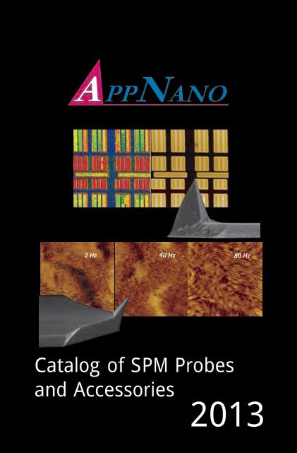
2 Hz 40 Hz 80 Hz<strong>Catalog</strong> of SPM <strong>Probes</strong>and Accessories2013
Table of ContentsProbe Info &Selection GuideSilicon <strong>Probes</strong>Coated <strong>Probes</strong> Special/Custom Silicon Nitride Tip View <strong>Probes</strong><strong>Probes</strong> (ACCESS)Membranes /StandardsSTM <strong>Probes</strong>General Information 3-7ACT Tapping 8ACL Long Tapping 9ACST Soft Tapping 10FORT Force 11SHOCON Short Contact 12SICON Contact 13ACCESS Tip View 14-17Ultra-High Frequency (UHF) <strong>Probes</strong> Fast Scanning 18Hydra (Silicon Nitride) <strong>Probes</strong> Soft & Liquid 19-21Hydra-All Soft & Liquid 22VScan Soft Tapping 23Nitra-All Soft & Liquid 24Plateau <strong>Probes</strong> Force 25Ball <strong>Probes</strong>/Colloidal <strong>Probes</strong> Force 26-27High Aspect Ratio Tilted (HART) <strong>Probes</strong> Deep Features 28-29FCL Calibration 30Doped Diamond <strong>Probes</strong> Conducting 31ANSCM (Electrical/EFM) <strong>Probes</strong> EFM 32Magnetic (MAGT) <strong>Probes</strong> MFM 33Step-Height Standards 35Membranes & Nanopores 36-37STM <strong>Probes</strong> & Etcher STM 38-39Custom Fabrication 40Quick Reference Chart 41-43Cover images: (top) SRAM sample. 50μm scan – Topography. Images acquired with a Nano-Observer AFM and ResiScope II. Courtesy of CSInstruments.eu and ScienTec, acquired with aDoped Diamond DD-ACTA probe.(bottom) Phase images of SEBS Block Copolymer sample, courtesy of Brian D. Huey and VarunVyas of the Huey AFM Lab at the University of Connecticut. Acquired using an ACCESS-UHFprobe using a scan rate of 2 Hz, 40 Hz, and 80 Hz and a drive frequency of 850 kHz.<strong>Applied</strong> <strong>NanoStructures</strong>, Inc. 2013 Page 2
<strong>AppNano</strong> Patented Wafer Form<strong>AppNano</strong> developed a patentedwafer form with major improvements.This new form allowsfor open tweezers accessto the bottom half of the AFMprobe chip. Open access makesremoval easy without damagingthe cantilever or tip. Thin 50 μmhorizontal silicon beams holdthe chip in place while remainingeasy to break when force isapplied for removal.The “old-style” wafer form, offered by most manufacturers,makes the removal of chips difficult andtedious. The use of tweezers is impaired by thickbeams leaving little area for tweezers. Additionally,horizontal beams tend to be nearly 250 µm thick.Removal of tips requires more force which oftencauses beams to shatter. The resulting fragments area serious problem as they can destroy the tip apex ofother probes on the wafer. The traditional waferform has often been a problem and reduces thebenefits of bulk purchasing.<strong>AppNano</strong> WaferFormThe chip holding beams arestrategically positioned. Theyallow for maximum access tothe probes while utilizingtweezers. The beam placementalso maintains a sturdy holdingstructure for the probes.www.appnano.com | Tel: 408-567-0115 | sales@appnano.com Page 3
Probe Info &Selection GuideProbe Chip & Wafer SpecificationsAPPNANO <strong>Probes</strong> Fit All CommercialAFM SystemsAlignment Grooves - <strong>AppNano</strong> <strong>Probes</strong> areavailable with and without alignment grooves.The groove locations on our probe chips havebeen adjusted such that the laser spot falls atthe extreme end of the cantilever, irrespectiveof the length of the cantilever, when used withalignment chips.Agilent Technologies(Molecular Imaging, PacificNanotechnology)AFM WorkshopAlfantacAmbios Tech (Quesant)Asylum ResearchBruker (AXS, SIS, Veeco Instruments,Digital Instruments,Thermo-Microscopes, TopoMetrix)JeolProbe Chip Dimensions -JPK InstrumentsThe dimensions of theprobe chip are 3400 µmNanonicsx 1600 µm x 315 µmNanosurf(Length x Width x Thickness).Alignment GroovesNovascanNT-MDTTerms & ConditionsPark Systems- FCA: Origin- Payment: Prepaid or Net 30 days upon approved Seiko Instrumentscredit.WiTek- Freight Charges: All freight charges are to be paid bythe buyer.- Warranty: Six months after shipping subject to standard storages and handlingconditions. Contact <strong>AppNano</strong> customer support for details.- Delivery: All products are shipped on a best effort basis depending upon availability.- Acceptance: Acceptance of these products is assumed if not returned to <strong>AppNano</strong>AFM <strong>Probes</strong> within 30 days of receipt of goods. All prices and specifications aresubject to change. Specifications listed are the nominal specifications for each product.Visit our website for specification ranges. If certain specifications are critical toyour application, please contact our technical staff to verify specifications prior topurchase. For a complete copy of our Terms & Conditions, contactinfo@appnano.com.<strong>Applied</strong> <strong>NanoStructures</strong>, Inc. 2013 Page 4CSIHitachi
Standard Silicon <strong>Probes</strong>Material - <strong>AppNano</strong> silicon probes are manufactured out of prime grade,low resistivity (0.010 to 0.025 Ω-cm), n-type Antimony doped, single crystalsilicon. Well-established silicon technology combined with novel microfabricationprocesses are the key ingredients for achieving high qualitymonolithic probes with unprecedented tip sharpness.Silicon ProbeInformationTip - <strong>AppNano</strong> silicon probe tips areavailable in tetrahedral and triangularpyramid shape.Tetrahedral Tip: Tip height range is 14 µm to 16 µm Tip offset range is 15 µm to 25 µm Side angle is 18° Front plane angle is 31° and backplane is 9°Cantilever - The length of the cantileveris measured from the chip body tothe tip center. The width is the averagewidth of the cantilever.HeightTop ViewLengthOffsetWidthSide ViewThicknessTip View <strong>Probes</strong>: All ACCESS series probes havetriangular shaped tips. These tips are at theextreme end of the cantilever. Tip height range is 14 to 16 µm Side angle from front view is 15° Apex half cone angle is 11°Coatings - We also offer tailored specification and specialized metal coatingsof tip and cantilever, such as Aluminum, Gold, Platinum, Nickel, and others.Probe Packaging - <strong>AppNano</strong> <strong>Probes</strong> are packed andshipped in conducting and ESD safe boxes. Ourstandard package sizes are 5, 10, 20, 50, 200 and fullwafer (410+) probes.www.appnano.com | Tel: 408-567-0115 | sales@appnano.com Page 5
ServicesOfferedMounted <strong>Probes</strong>Services OfferedSome AFM systems require AFM probes that have been pre-mounted on specialprobe holders. <strong>AppNano</strong> can supply pre-mounted probes for most majorAFM systems for a small fee. <strong>AppNano</strong> has the technology and fixtures tocorrectly mount any of our AFM probes for systems manufactured by AmbiosTechnology, Bruker (including TopoMetrix, Park and Digital Instruments), PacificNanotechnology (PNI), Park Systems, and Quesant. The type of systemmust be specified at the time of ordering.Imaging and Analytical ServicesIn addition to probe production, <strong>AppNano</strong> offers a variety of imaging, analytical,and characterization services using the state-of-the-art equipment in ourfacility. Possible sample types for this process include polymers, metallurgicalsamples, electronic materials, ceramics, and particles and contaminants onvarious surfaces.Available services: Atomic Force Microscopy (AFM) Field Emission Scanning Electron Microscopy (FE-SEM) Focused Ion Beam (FIB)Contact info@appnano.com for more information.<strong>Applied</strong> <strong>NanoStructures</strong>, Inc. 2013 Page 6
Probe Option: Super Sharp (SS)<strong>AppNano</strong> produces Super Sharp (SS) <strong>Probes</strong> with a proprietary process; theresulting tips achieve an ultra-small curvature radius (1-2nm). <strong>AppNano</strong>Super Sharp probes yield enhanced resolution images.Tip SpecificationsShape: PyramidalHeight (µm): 14-16ROC (nm): 1-2Cantilever SpecificationsMaterial: SiShape: RectangularReflex Coating: None, AlStandard Silicon Probe OptionsProbe Option: Tipless (TL)<strong>AppNano</strong> probes are also available in a configuration where there is no tip onthe cantilever. These probes are used for custom applications.Cantilever SpecificationsMaterial: SiShape: RectangularReflex Coating: None, AlStandardOptionsStandard Coating OptionsProbe TypeNoCoatingAluminum,Reflex SideGold,Reflex SideGold,Both SidesStandard Yes Yes Yes YesSuper Sharp Yes Yes No NoTipless Yes Yes No NoCustom Options Available— Custom gold and platinum coatings availableupon request. For details, contact by phone or email.www.appnano.com | Tel: 408-567-0115 | sales@appnano.com Page 7
Probe Model: ACT SeriesSilicon Tapping Mode <strong>Probes</strong>ACT Series <strong>Probes</strong> are designed for non-contact, tapping, and close contactmode applications in air and fluid. ACT probes have a high frequency thatallows faster scanning.Tapping / NoncontactModeCantilever ParameterNominal ValueSpring Constant (N/m) 37Frequency (kHz) 300Length (µm) 125Width (µm) 30Thickness (µm) 4Tip SpecificationsMaterial: SiShape: PyramidalHeight (µm): 14-16Front Plane: 31°Back Plane: 9°Probe Type Description Tip ROCACTACTAACTGStandard ACT ProbeReflex side, Al coated, ACT ProbeReflex side, Gold coated, ACT Probe6nm(Guaranteed
Probe Model: ACL SeriesACL Series <strong>Probes</strong> are designed for non-contact, tapping mode, intermittentcontact, and/or close contact applications. The long ACL cantileverallows larger laser clearance. These probes are available with and withoutAl coating on the reflex side.Cantilever ParameterNominal ValueSpring Constant (N/m) 58Frequency (kHz) 190Length (µm) 225Width (µm) 40Thickness (µm) 7.8Long Silicon Tapping Mode <strong>Probes</strong>Tip SpecificationsMaterial: SiShape: PyramidalHeight (µm): 14-16Front Plane: 31°Back Plane: 9°Probe Type Description Tip ROCLong Tapping /Non-contact ModeACLACLAACLGStandard ACL ProbeReflex side, Al coated, ACL ProbeReflex side, Gold coated, ACL Probe6nm(Guaranteed
Probe Model: ACST SeriesSilicon Soft Tapping Mode <strong>Probes</strong>ACST Series <strong>Probes</strong> are designed for soft tapping or non-contact mode applications.ACST probes are moderately soft with a mid-range resonancefrequency.Soft Tapping / Non-contact ModeCantilever ParameterNominal ValueSpring Constant (N/m) 7.8Frequency (kHz) 150Length (µm) 150Width (µm) 28Thickness (µm) 3Tip SpecificationsMaterial: SiShape: PyramidalHeight (µm): 14-16Front Plane: 31°Back Plane: 9°Probe Type Description Tip ROCACSTACSTAACSTGStandard ACST ProbeReflex side, Al coated, ACST ProbeReflex side, Gold coated, ACST Probe6nm(Guaranteed
Silicon Force Modulation Mode <strong>Probes</strong>Probe Model: FORT SeriesFORT Series <strong>Probes</strong> are designed for force modulation applications. FORTprobes’ medium frequency and spring constantmakes them ideal for Force Modulation Mode.Cantilever ParameterNominal ValueSpring Constant (N/m) 1.6Frequency (kHz) 61Length (µm) 225Width (µm) 27Thickness (µm) 2.7Tip SpecificationsMaterial: SiShape: PyramidalHeight (µm): 14-16Front Plane: 31°Back Plane: 9°Probe Type Description Tip ROCForce ModulationMode <strong>Probes</strong>FORTFORTAFORTGStandard FORT ProbeReflex side, Al coated, FORT ProbeReflex side, Gold coated, FORT Probe6nm(Guaranteed
Short Silicon Contact Mode <strong>Probes</strong>Probe Model: SHOCON SeriesSHOCON Series <strong>Probes</strong> are designed for contact mode applications with ashorter length, providing better sensitivity without compromising onspring constant requirements.Short ContactMode <strong>Probes</strong>Cantilever ParameterNominal ValueSpring Constant (N/m) 0.14Frequency (kHz) 21Length (µm) 225Width (µm) 46Thickness (µm) 1.0Tip SpecificationsMaterial: SiShape: PyramidalHeight (µm): 14-16Front Plane: 31°Back Plane: 9°Probe Type Description Tip ROCSHOCONSHOCONASHOCONGStandard SHOCON ProbeReflex side, Al coated, SHOCON ProbeReflex side, Gold coated, SHOCON Probe6nm(Guaranteed
Silicon Contact Mode <strong>Probes</strong>Probe Model: SICON SeriesSICON Series <strong>Probes</strong> are for contact mode applications. These probes havea long, thin cantilever allowing for a low spring constant and improved laserclearance.Cantilever ParameterNominal ValueSpring Constant (N/m) 0.29Frequency (kHz) 15Length (µm) 450Width (µm) 49Thickness (µm) 2.5Tip SpecificationsMaterial: SiShape: PyramidalHeight (µm): 14-16Front Plane: 31°Back Plane: 9°Probe Type Description Tip ROCContact Mode<strong>Probes</strong>SICONSICONASICONGStandard SICON ProbeReflex side, Al coated, SICON ProbeReflex side, Gold coated, SICON Probe6nm(Guaranteed
Probe Model: ACCESS-CContact Mode—Tip View <strong>Probes</strong>ACCESS-C <strong>Probes</strong> are sharp silicon probes designed to allow a direct opticalview of the AFM tip when imaging. ACCESS-C is intended for use in contactmode.Cantilever ParameterNominal ValueSpring Constant (N/m) 0.3ACCESS Tip View<strong>Probes</strong>Frequency (kHz) 16Length (µm) 450Width (µm) 49.5Thickness (µm) 2.5ROC (nm)
Probe Model: ACCESS-NCTapping Mode—Tip View <strong>Probes</strong>ACCESS-NC <strong>Probes</strong> are sharp silicon probes designed to allow a direct opticalview of the AFM tip when imaging. ACCESS-NC is intended for use intapping/non-contact mode.Cantilever ParameterNominal ValueSpring Constant (N/m) 78Frequency (kHz) 300Length (µm) 150Width (µm) 54Thickness (µm) 5.2ROC (nm)
Probe Model: ACCESS-FMForce Modulation—Tip View <strong>Probes</strong>ACCESS-FM <strong>Probes</strong> are sharp silicon probes designed to allow a direct opticalview of the AFM tip when imaging. ACCESS-FM are ideal for ForceModulation Mode.Cantilever ParameterNominal ValueACCESS Tip View<strong>Probes</strong>Spring Constant (N/m) 2.7Frequency (kHz) 60Length (µm) 245Width (µm) 52Thickness (µm) 2.8ROC (nm)
Conductive—Tip View <strong>Probes</strong>Conductive ACCESS <strong>Probes</strong>Conductive ACCESS <strong>Probes</strong> are silicon probes with conductive coatings (PtIrand Gold) designed to allow a direct optical view of the AFM tip when imaging.ACCESS-EFM is coated with PtIr, ACCESS-FM-GG is coated with gold.Both probes are ideal for Electrical Force Microscopy.Coating SpecificationsReflex Side:Tip Side:Coating Options:CoatedCoatedPtIr or GoldCantilever Parameter Nominal ValueSpring Constant (N/m) 2.7Frequency (kHz) 60Length (µm) 245Width (µm) 52Thickness (µm) 2.8ROC (nm) 30Ordering Codes15.13° 14.52°Tip SpecificationsMaterial : SiliconHeight (µm): 14-16Tip Tilt: 17°Apex Half-ConeAngle: 11°Front Plane: 15°ACCESS Tip View<strong>Probes</strong>Pt-Ir CoatedGold Coated<strong>Probes</strong>ACCESS-EFM-10 ACCESS-FM-GG-1010ACCESS-EFM-20 ACCESS-FM-GG-2020ACCESS-EFM-50 ACCESS-FM-GG-5050ACCESS-EFM-200 ACCESS-FM-GG-200200ACCESS-EFM-W ACCESS-FM-GG-W410+www.appnano.com | Tel: 408-567-0115 | sales@appnano.com Page 17
Ultra-High Frequency <strong>Probes</strong>Probe Model: ACCESS-UHF Fast-Scan SeriesACCESS-UHF Fast-Scan (UHF) Series <strong>Probes</strong> are designed for fast and highresolution imaging. The reflex side can optionally be coated with aluminum.Tip SpecificationsShape: PyramidalHeight (µm): 8-12ROC (nm): 6Cantilever SpecificationsUHF Fast-Scan<strong>Probes</strong>Material:Shape:Coating:SiRectangularNone or AlParameterNominal ValueSpring Constant (N/m) 115Frequency (kHz) 1100Length (µm) 55Width (µm) 26Thickness (µm) 2.8Tip ROC (nm)
HYDRA Probe SeriesThe HYDRA Series is a unique series of silicon nitride probes, with a proprietarydesign by <strong>AppNano</strong>. The probe consists of a silicon chip, siliconnitride cantilever, and silicon tetrahedral tip.Ordering InformationExample Part Number: HYDRA6V-100NSilicon Nitride (Soft) <strong>Probes</strong>Thickness:2 for 200nm4 for 400nm6 for 600nmHYDRA 6 V - 100 NWidth:N for NarrowW for WideShape:V - for V-shapeR - for RectangularAdditional OptionsReflex Coating:G for GoldLength:50 for 50 µm100 for 100 µm200 for 200 µmExample: HYDRA6V-100NGNitride <strong>Probes</strong>Tip & Reflex Coating:GG for Gold-GoldExample: HYDRA6V-100NGGTipless Option:TL for Tip-LessExample: HYDRA6V-100N-TLwww.appnano.com | Tel: 408-567-0115 | sales@appnano.com Page 19
Silicon Nitride (Soft) <strong>Probes</strong>Probe Model: HYDRA (R) Rectangular SeriesThe HYDRA R-Series <strong>Probes</strong> are rectangular nitride cantilevers with a sharpsilicon tip designed for force-distance applications. These probes can alsobe used for tapping mode and contact mode in an air or fluid medium.Nitride <strong>Probes</strong>Tip SpecificationsMaterial: SiliconShape: TetrahedralHeight (µm): 4-6ROC (nm):
Probe Model: HYDRA V-Shaped SeriesThe HYDRA V-Series <strong>Probes</strong> are V-shaped nitride cantilevers with a sharpsilicon tip for imaging soft samples. These probes can be used for forcedistancemode, tapping mode, or contact mode in air or liquid.Tip SpecificationsMaterial: SiliconShape: TetrahedralHeight (µm): 4-6ROC (nm):
Probe Model: Hydra-All SeriesThe Hydra-All Probe is a 4-in-1 probe chip with four cantilevers of varyingspring constants and lengths. The probe is designed for work with soft materialsand can be used to handle various functions.Tip SpecificationsMaterial: SiliconShape: TetrahedralHeight (µm): 4-6ROC (nm):
Probe Model: VScan SeriesThe VScan Series <strong>Probes</strong> are V-shaped nitride cantilevers with a sharp silicontip designed for SCAN-ASYST* Mode. These probes can also be usedfor tapping mode and contact mode in air or fluid mediums.Tip SpecificationsMaterial: Silicon NitrideShape: TetrahedralHeight (µm): 4-6ROC (nm):
Probe Model: Nitra-All SeriesThe Nitra-All Probe is a 4-in-1 probe chip with four silicon nitride probes ofvarying spring constants and lengths. The cantilevers and tips are monolithicsilicon nitride material. The probe is designed for work with soft materialsand can be used to handle various functions. The reflex side iscoated with gold.Tip Specifications4-Silicon Nitride Cantilevers on 1 Probe ChipMaterial: Silicon NitrideShape: TetrahedralHeight (µm): 10ROC (nm):
Silicon Plateau (Blunt Radius) <strong>Probes</strong>Probe Model: Plateau (PTU) SeriesPlateau (PTU) Series <strong>Probes</strong> are produced with a flat top and a conical tip,providing a well defined contact area. The Plateau series is available withoptional tilt compensation.CantileverACTACTAFORTFORTASICONSICONADescription79 N/m, 300 kHz, Uncoated79 N/m, 300 kHz, Al reflex3.4 N/m, 60 kHz, Uncoated3.4 N/m, 60 kHz, Al reflex0.31 N/m, 13 kHz, Uncoated0.31 N/m, 13 kHz, Al reflexOrdering InformationTip SpecificationsMaterial: SiShape: PlateauRadius (µm): 1.8Height (µm): 14-18Front Plane: 2°Back Plane: 9°ACT-PTUACTA-PTUFORT-PTUFORTA-PTUSICON-PTUSICONA-PTUTipsACT-PTU-10ACTA-PTU-10FORT-PTU-10FORTA-PTU-10SICON-PTU-10SICONA-PTU-1010ACT-PTU-20ACT-PTU-50ACTA-PTU-20ACTA-PTU-50FORT-PTU-20FORT-PTU-50FORTA-PTU-20FORTA-PTU-50SICON-PTU-20SICON-PTU-50SICONA-PTU-20SICONA-PTU-502050Plateau <strong>Probes</strong>A tilt-compensated PTU probe. Contactsales@appnano.com for more information.www.appnano.com | Tel: 408-567-0115 | sales@appnano.com Page 25
Probe Model: Ball <strong>Probes</strong>Carbon Ball Tip on Silicon <strong>Probes</strong>Ball <strong>Probes</strong> are designed for applications that require hard contact with thesample. The tip apex is created using Electron Beam Deposited high densitycarbon. It is hemispherical in shape and has an extremely smooth surface.Ball TypeBall Diameter-B20 10-30nm-B35 25-45nm-B50 40-60nm-B100 90-110nm-B150 135-165nmBall probes can be ordered withoptional aluminum or gold coatingon the reflex side.Tip SpecificationsMaterial: Si/High Density CarbonShape:BallHeight (µm): 14-16Front Plane: 31°Back Plane: 9°Ordering InformationBall <strong>Probes</strong>CantileverModelFORT (1.6 N/m, 60 kHz)ACT (37 N/m,300 kHz)Probe Type-B20 -B35 -B50 -B100 -B150FORT-B20FORT-B35FORT-B50ACT-B20 ACT-B35 ACT-B50FORT-B100ACT-B100FORT-B150ACT-B150SICON (0.29 N/m, 15 kHz)SICON-B20SICON-B35SICON-B50SICON-B100SICON-B150<strong>Applied</strong> <strong>NanoStructures</strong>, Inc. 2013 Page 26
Probe Model: COLLOIDAL <strong>Probes</strong>Colloidal Probe Atomic Force Microscopy requires a tip of known shape tobe mounted cleanly on a consistently reproducible cantilever. Theseprobes are known as “Colloidal <strong>Probes</strong>” and are used to study colloidalinteractions between two surfaces and to quantify the interactive properties.The tip is formed using a spherical, colloidal particle attached to atipless cantilever.Colloidal Probe Custom Manufacturing Ordering InformationTipless Cantilever Types:ACL, ACT, FORT, HYDRA,SHOCON, SICONColloidal Particle Options:Type: Au, BSG, SiO, PSDiameter: A - 5 µm to 9 µmB - 10 µm to 14 µmC - 15 µm to 19 µmD - 20 µm or moreManufacturing:Attach the spheres to the tipless cantileverusing high precision 6 axis micromanipulatorswith 1,000x opticsSpherical Tip on CantileversCoating Options:Reflex Side: A (Al), G (gold)Tip Side : G (gold)Colloidal <strong>Probes</strong>Model Number InformationType-Size-Coating-Quantity*Example: The part # for 5 ofthe 12 µm diameter glasssphere colloidal probes withgold coating on both sides is -SICON-BSG-B-GG-5** Minimum order is 5 probes perbox of each type orderedwww.appnano.com | Tel: 408-567-0115 | sales@appnano.com Page 27
High Aspect Ratio <strong>Probes</strong>High Aspect Ratio Tilted <strong>Probes</strong><strong>AppNano</strong> manufactures probes with various spike lengths and widths fortrenches and deep features. SPM/AFM instrument manufacturers usedifferent probe chip mounting angles. <strong>AppNano</strong> provides options to meetall commercial AFM systems. Additionally, we can fabricate HART probesto meet custom dimensions.Tilt CompensationSpike Tilt: HART probe spikes areoffered with three tilt variations(0°, 3°, 12°). By offsetting the AFMsystem’s natural mounting tilt, thespike is arranged perpendicular tothe surface.Ordering Information (Standard)Example Part Number: HART3-2-5High Aspect Ratio<strong>Probes</strong>Tilt Compensation:0 for 0° Tilt3 for 3° Tilt12 for 12° TiltHART3 - 2 - 5Spike Length:Length 1 µmLength 2 µmLength 4 µmLength 6 µmQuantity:5 Probe Box*50 Probe Box**Standard boxsizesOrdering Information (with Reflex Coating)Example Part Number: HARTA3-2-5Al Reflex Side CoatingHARTA3 - 2 - 5<strong>Applied</strong> <strong>NanoStructures</strong>, Inc. 2013 Page 28
Probe Model: HART SeriesHigh Aspect Ratio <strong>Probes</strong>HART Series <strong>Probes</strong> are designed for imaging or depth metrology of shallowfeatures 1, 2, 4 or 6 µm deep. The spike is tilt-compensated to enterthe trench vertically down. The spike angle is specified at 0, 3, or 12° .Spike PropertiesHeavily Doped(0.01—0.025Ω-cm) Single Crystal SiFocused Ion Beam MilledTip ROC:
Probe Model: FCL SeriesForce Calibration <strong>Probes</strong><strong>Applied</strong> <strong>NanoStructures</strong>' FCL Probe is a tipless force calibration probe withfive cantilevers. These probes are designed for the spring constant calibrationof SPM probes. The reflex side can optionally be coated with aluminum.Cantilever SpecificationsMaterial: SiShape: RectangularThickness (µm): 2.0Width (µm): 32Reflex Coating: None or AlHandle Chip SpecificationsLength (mm): 3.4Width (mm): 1.6Thickness (µm): 300ABCDECantileverFrequency(kHz)Spring Constant(N/m)Length (µm)A 14 0.12442B 60 0.98218Force ModulationMode <strong>Probes</strong>C 300 1296D 550 3069E 1000 7750Ordering InformationFCL-5 5FCL-10 10FCLA-5 5FCLA-10 10<strong>Applied</strong> <strong>NanoStructures</strong>, Inc. 2013 Page 30
Probe Model: Doped Diamond SeriesDoped Diamond (DD) <strong>Probes</strong> offers a unique combination of hardness andconducting tip. The tip side of these probes is coated with polycrystallinediamond. The diamond film is doped with boron to make it highly conducting.Tip SpecificationsShape: PyramidalHeight (µm): 14-16Aspect Ratio: 1.5-3.0ROC* (nm): 100-300Coating: 100nm Doped Diamond*Nominal specificationCantilever SpecificationsMaterial: SiShape: RectangularReflex Coating: AlParameterProbe TypeDD-ACTA DD-FORTA DD-SICONASpring Constant (N/m) 37 1.6 0.29Frequency (kHz) 300 61 15Length (µm) 125 225 450Width (µm) 30 27 49Thickness (µm) 4.0 2.7 2.5Ordering InformationDurable Conductive <strong>Probes</strong>NC FM EFM <strong>Probes</strong>DD-ACTA-10 DD-FORTA-10 DD-SICONA-10 10DD-ACTA-20 DD-FORTA-20 DD-SICONA-20 20DD-ACTA-50 DD-FORTA-50 DD-SICONA-50 50Doped Diamond<strong>Probes</strong>DD-ACTA-200 DD-FORTA-200 DD-SICONA-200 200DD-ACTA-W DD-FORTA-W DD-SICONA-W 410+www.appnano.com | Tel: 408-567-0115 | sales@appnano.com Page 31
Probe Model: ANSCM SeriesANSCM Series <strong>Probes</strong> are coated with PtIr on both sides for EFM applications.ANSCM-PT probes are for force modulation, ANSCM-PC probes arefor contact mode applications, and ANSCM-PA probes are for tappingmode. ANSCM-PA5 probes are designed for CAFM applications and have athicker PtIr coating to extend the probe’slifetime.ApplicationsConductive (PtIr) Coated <strong>Probes</strong>Electrical Force MicroscopyConducting Atomic Force MicroscopyKelvin Force MicroscopyPiezo Force MicroscopyScanning Capacitance MicroscopyShape: PyramidalHeight (µm): 14-16Coating: PtIrProbe TypeParameterANSCM-PA5ANSCM-PAANSCM-PTANSCM-PCSpring Constant (N/m) 37 37 2.7 0.29Frequency (kHz) 300 300 60 12Length (µm) 125 125 225 450Width (µm) 30 30 27 49Thickness (µm) 4.0 4.0 2.7 2.5Tip ROC (nm) 50 30 30 30PtIr Coated <strong>Probes</strong>Pt/Ir Thickness (nm) 50 25 25 25Ordering InformationStandard Package Size: 10, 20, 50, 200 and Wafer (410+)probesKey to Order Part Number: (Probe type) - (Package size)Example: (i) Part number to order 10 Force ModulationEFM <strong>Probes</strong> is: ANSCM-PT-10(ii) Part number to order 50 contact mode EFM probes:ANSCM-PC-50<strong>Applied</strong> <strong>NanoStructures</strong>, Inc. 2013 Page 32
Probe Model: MAGT SeriesMagnetic Coated (MFM) <strong>Probes</strong>MAGT Series <strong>Probes</strong> are for MFM applications. MAGT probes have a mediumcoercivity and medium moment, MAGT-LM probes have low momentand MAGT-HM probes have high moment magnetic material coatings.Tip SpecificationsShape: PyramidalHeight (µm): 14-16ROC* (nm): see belowCoating: see below ± 5nm*Nominal specificationCantilever SpecificationsMaterial: SiShape: RectangularReflex Coating: Cr-CoTip Coating: Cr-CoParameterValueSpring Constant (N/m) 2.7Frequency (kHz) 61Length (µm) 225Width (µm) 27Thickness (µm) 2.7Type Specification CoatingMAGT ROC (nm): 40 Cr-Co, 50nmMAGT-LM ROC (nm): 25 Cr-Co, 15nmMAGT-HM ROC (nm): 75 Cr-Co, 150nmOrdering InformationRegularMAGT-10MAGT-20Low MomentMAGT-LM-10MAGT-LM-20High Moment <strong>Probes</strong>MAGT-HM-10 10MAGT-HM-20 20Magnetic Coated<strong>Probes</strong>MAGT-50MAGT-LM-50MAGT-HM-50 50MAGT-200MAGT-LM-200MAGT-HM-200 200MAGT-W MAGT-LM-W MAGT-HM-W 410+www.appnano.com | Tel: 408-567-0115 | sales@appnano.com Page 33
Pictures taken with <strong>AppNano</strong> <strong>Probes</strong>CustomerImagesNoncontact AFM image of silkproteins deposited from anaqueous solution. Image acquiredby Dr. HannesSchniepp of College of Williamand Mary, using one of ourACTA probes.Artificial spin ice sample. 7 μm scan – Topography and MFM.Sample courtesy of P. Vavassori of CIC Nanogune – SanSebastian - SPAIN. Images acquired with a Nano-ObserverAFM (MFM). Courtesy of CSInstruments.eu and ScienTec,taken using an MAGT probe.Graphene sample. 10μm scan –Phase. Images acquired with aNano-Observer AFM. Courtesyof CSInstruments.eu andScienTec, acquired using aFORT probe.<strong>Applied</strong> <strong>NanoStructures</strong>, Inc. 2013 Page 34
Standards Model: SHS-1, SHS-0.1Step Height StandardsStep Height Standards (SHS) are designed for X,Y, and Z calibration ofscanning probe microscopes and profilometers. Our Step Height Standardfeatures are available in two heights and are defined in thermally grownsilicon dioxide on silicon substrate. A layer of Cr is deposited on the standardmodel to harden the surface; a version without Cr, the SHS-OX series,is also available.Feature Description DetailsA Square Grid 3 μm pitchB Square Grid 10 μm pitchC Grating 10 μm pitchD Grating 3 μm pitchE Grating 50 μm pitchF Grating 20 μm pitchG Square Pad 100 μm x 100 µmH Rectangular Line 1000 µm x 200nmOrdering InformationPart NumberStep HeightSHS-1 1 µmSHS-0.1100nmSHS-OX-1 1 µmSHS-OX-0.1100nmStep HeightStandardswww.appnano.com | Tel: 408-567-0115 | sales@appnano.com Page 35
Membrane WindowsMembrane Model: SIWD, NIWD, OXWD<strong>Applied</strong> <strong>NanoStructures</strong>’ SIWD Membrane is made with silicon, NIWDMembrane is made with low stress silicon nitride, OXWD Membrane ismade with silicon oxide which can be coated with various materials accordingto customer request. Additionally, the size of the chip and window andthickness of the membrane can be varied to fit different applications.Window Side SEMmembranewindowCross-sectional viewParameters for ChipValue for ChipNominal Minimum MaximumThickness (µm) 300 290 310Width & Length (µm) 6000 x 6000 5950 x 5950 6050 x 6050CoatingsVarious Coatings AvailableParameters forWindowWDMembrane SizeWDSThickness (nm) 200 200Membrane Size (µm) 200 x 200 20 x 20Window Size (µm) 600 x 600 450 x 450Ordering InformationExample Part Number# of ChipsMembranesSIWD-5 / SIWDS-5 5SIWD-20 / SIWDS-20 20SIWD-100 / SIWDS-100 100<strong>Applied</strong> <strong>NanoStructures</strong>, Inc. 2013 Page 36
Membrane Model: PORE<strong>AppNano</strong> PORE products are designed for various biological applications.Our nanopores are microfabricated using single crystal Silicon (SIWD), SiliconNitride (NIWD), or Silicon Oxide (OXWD) membranes. Nanopores canbe ordered with a single pore, or in a 2x2 or 5x5 array.Membrane MaterialEtched NanoporesSiliconSilicon NitrideSilicon OxideSINIOXArrangement of PoresSingle Pore 012x2 Array 225x5 Array 55PORE-SI-01-020Specify regular (WD) or small(WDS) window size whenordering.Nanopore Diameter20nm 020100nm 100200nm 200Single PoreOrdering Information2x2 Array5x5 ArrayExample Part Number# of ChipsPORE-SI-01-020 2PORE-SI-01-100 5PORE-SI-01-200 5Nanoporeswww.appnano.com | Tel: 408-567-0115 | sales@appnano.com Page 37
Etched Tungsten <strong>Probes</strong> for STMProbe Model: STM-W<strong>AppNano</strong> etchedSTM probes aremade from 99.95%tungsten wire (0.25mm in diameter).The probesare produced bycomputer controlledelectrochemicaletchingand result inprobes with a tipradius of less than20nm.Ordering InformationPart Number # of TipsSTM-W-5 5Probe Model: STM-Pt<strong>AppNano</strong> etchedSTM probes aremade from99.95% platinumwire (0.25 mmdiameter). Theprobes are producedby cuttingwire to achieve atip radius of lessthan 20nm.Ordering InformationPart Number# of TipsSTM-Pt-5 5Cut Platinum <strong>Probes</strong> for STMEtched Platinum <strong>Probes</strong> for STMSTM <strong>Probes</strong><strong>AppNano</strong> can provide computer controlled, custom etched STM probesmade from 99.95% platinum wire. Quotations and details can be requestedby email; please contact sales@appnano.com.<strong>Applied</strong> <strong>NanoStructures</strong>, Inc. 2013 Page 38
STM Tip EtcherProduct: STM Tip EtcherThe <strong>AppNano</strong> STM Tip Etcher is a compact, easy to use system for etchingcustom STM tips with a user-controlled timed etch. The etcher features anautomatic tip etch stop, an automatic dip and retract, and a live tip etchview. The machine uses pulse etching technology for highly controlled andreproducible tip ROC and aspect ratio. The pulse width is variable for creatingcustom tip shapes. An optional electroplating mode is capable ofnanometer scale metal deposition.Features:Etch type: DC PWMSelectable etch Voltage: 1.5V to 12VVoltage display: 3.5 digit DVMCurrent max: 1ASlow etch: selectable 0.1% to 4% "on" at 10HzFast etch: selectable 4% to 40% "on" at 100HzOptical view: ~200X digital microscopeSurface detect: electronic detection of the etch liquid surface w/ LED outputTip etch control: Linear Servo with 15 mm travel, 0.02 mm step resolutionTip taper distance: 2 mm (can be specified shorter or longer).For more information, contact sales@appnano.com.www.appnano.com | Tel: 408-567-0115 | sales@appnano.com Page 39STM Tip Etcher
Custom Fabrication ProfileCustom MEMS & NanofabricationIn addition to providing you with our standard catalog of products, <strong>Applied</strong><strong>NanoStructures</strong> enjoys working with customers to develop new probesand devices for advanced applications. Our experienced Research and Developmentteam takes pride in using our knowledge of silicon nanofabricationtechnology to realize these new ideas.Advanced ManufacturingClean Room FacilityWet Chemical ProcessingDiffusion / Oxidation ProcessingMetallization (Al, Cr, Ti, Au, Ni, Ag, PtIr, etc.)Focused Ion BeamDry Etching ProcessingPhysical Vapor DepositionPhotolithographyOptical and Electrical CharacterizationScanning Probe and Scanning ElectronMicroscopy ImagingProcess DesignR&D, Manufacturing & QA CleanRoomsSuited for rapid prototyping as well asbatch processing.OEM / Custom NanofabricationNano Thermal Analysis <strong>Probes</strong>Piezoresistive CantileversCustom MEMS/NanofabricationComplete facility to develop, manufacture,qualify and test MEMS devices.Continual upgrades to the facility withnew equipmentFlat Tip <strong>Probes</strong>MOSFET CantileversTall Tip <strong>Probes</strong>Custom MEMS devicesPlease contact us at info@appnano.comif you would like to discuss the creation of a custom product.<strong>Applied</strong> <strong>NanoStructures</strong>, Inc. 2013 Page 40
Application Probe Model DescriptionHighResolutionImagingChart of <strong>Probes</strong>CantileverLength (µm)Spring Constant(N/m)Resonance Frequency(kHz)ACT-SS Tapping Mode, Super Sharp Probe 125 37 300 AACL-SS Long, Tapping Mode, Super Sharp Probe 225 58 190 AACST-SS Soft Tapping Mode, Super Sharp Probe 150 7.8 150 AFORT-SS Force Modulation, Super Sharp Probe 225 1.6 61 ASHOCON-SS Short, Contact Mode, Super Sharp Probe 225 0.14 21 ASICON-SS Contact Mode, Super Sharp Probe 450 0.29 15 AOptionsUltra-HighFrequencyPlateau<strong>Probes</strong>ACCESS-UHF Ultra-High Frequency <strong>Probes</strong> 55 115 1100 AACT-PTU High Frequency Plateau <strong>Probes</strong> 125 79 300 N/AFORT-PTU Medium Frequency Plateau <strong>Probes</strong> 225 3.4 60 N/ASICON-PTU Low Frequency Plateau <strong>Probes</strong> 450 0.31 13 N/AACTA-B50 Tapping Mode, 50nm Ball 125 37 300 ABall <strong>Probes</strong>FORTA-B50 Force Modulation Mode, 50nm Ball 225 1.6 61 ASICONA-B50 Contact Mode, 50nm Ball 450 0.29 15 AColloidal<strong>Probes</strong>ACTA-BSG-A ACTA Tipless with BSG Colloidal, Size A 125 37 300 A, G, GGFORTA-BSG-A FORTA Tipless with BSG Colloidal, Size A 225 1.6 61 A, G, GGSICONA-BSG-A SICONA Tipless with BSG Colloidal, Size A 450 0.29 15 A, G, GGOption Definitions: A = Aluminum Reflex Coating; C = Custom Tilt & Spike Length; G = Gold Reflex Coating; TL = Tiplesswww.appnano.com | Tel: 408-567-0115 | sales@appnano.com Page 41
Application Probe Model DescriptionElectric ForceMicroscopyMagneticForceMicroscopyTip ViewDopedDiamondChart of <strong>Probes</strong>CantileverLength (µm)Spring Constant(N/m)Resonance Frequency(kHz)ANSCM-PA High Spring Constant EFM Probe 125 37 300 N/AANSCM-PT Medium Spring Constant EFM Probe 225 1.6 61 N/AANSCM-PC Low Spring Constant EFM Probe 450 0.29 15 N/AMAGT-LM Low Moment MFM <strong>Probes</strong> 225 1.6 61 N/AMAGT Medium Moment MFM <strong>Probes</strong> 225 1.6 61 N/AMAGT-HM High Moment MFM <strong>Probes</strong> 225 1.6 61 N/AOptionsACCESS-NC Non-Contact/Tapping Mode <strong>Probes</strong> 150 78 300 A, GGACCESS-FM Force Modulation <strong>Probes</strong> 245 2.7 60 AACCESS-EFM Electric Force Mode <strong>Probes</strong> 245 2.7 60 GG, PtIrACCESS-C Contact Mode <strong>Probes</strong> 450 0.30 16 ADD-ACTA Tapping Mode or Hard Contact Mode 125 37 300 N/ADD-FORTA Force Modulation Mode 225 1.6 61 N/ADD-SICONA Contact Mode Probe 450 0.29 15 N/AHigh AspectRatioHART0 No Tilt Compensation, 1, 2, 4 µm spike 125 37 300 A, CHART3 3° Tilt Compensation, 1, 2, 4 µm spike 125 37 300 A, CHART12 12° Tilt Compensation, 2, 4, 6 µm spike 125 37 300 A, COption Definitions: A = Aluminum Reflex Coating; C = Custom Tilt & Spike Length; G = Gold Reflex Coating; TL = Tipless<strong>Applied</strong> <strong>NanoStructures</strong>, Inc. 2013 Page 42
Application Probe Model DescriptionNon-Contact /TappingModeContactModeForce CurveLiquid4 in 1 <strong>Probes</strong>Chart of <strong>Probes</strong>CantileverLength (µm)Spring Constant(N/m)Resonance Frequency(kHz)OptionsACT Silicon Tapping Mode Probe 125 37 300 A, G, GG, TLACL Long Cantilever Tapping Mode Probe 225 58 190 A, G, GG, TLFORT Force Modulation Mode Probe 225 1.6 61 A, G, GG, TLACST Silicon Soft Tapping/Contact Mode Probe 150 7.8 150 A, G, GG, TLHYDRA6R-100N Silicon Nitride Probe, Rectangular CantileverHYDRA6V-100N Silicon Nitride Probe, V-Shape, NarrowCantileverHYDRA6V-100W Silicon Nitride Probe, V- Shape, Wide Cantilever100 0.284 66 G, GG, TL100 0.292 66 G, GG, TL100 0.405 67 G, GG, TLSICON Silicon Contact Mode Probe 450 0.29 15 A, G, GG, TLSHOCON Short Cantilever Contact Mode Probe 225 0.14 21 A, G, GG, TLHYDRA6R-200N Silicon Nitride, Rectangular Cantilever 200 0.035 17 G, GG, TLHYDRA6V-200N Silicon Nitride, V- Shape, Narrow Cantilever 200 0.045 17 G, GG, TLHYDRA6V-200W Silicon Nitride, V-Shape, Wide Cantilever 200 0.081 17 G, GG, TLHYDRA2R-100N Nitride Probe, Rectangular Cantilever 100 0.011 21 G, GG, TLHYDRA2R-50N Nitride Probe, Rectangular Cantilever 50 0.084 77 G, GG, TLVScan-Air Silicon Nitride Probe, V-Shape 100 0.292 66 AVScan-Liquid Silicon Nitride Probe, V-Shape 65 0.59 150 GHydra-All Four Silicon Nitride <strong>Probes</strong> on One Chip: HYDRA6V-100N, 100W, 200N, 200W GNitra-All Four <strong>Probes</strong> with Silicon Nitride Cantilevers and Silicon Nitride Tips on One Chip: HYDRA6V N/A-100N, 100W, 200N, 200WOption Definitions: A = Aluminum Reflex Coating; C = Custom Tilt Compensation & Spike Length; G = Gold Reflex Coating; GG = GoldReflex & Tip Coating; TL = Tiplesswww.appnano.com | Tel: 408-567-0115 | sales@appnano.com Page 43
In 2013, we will be expanding our operations by opening a newmanufacturing facility in Mountain View, CA. The new space containsa new, state of the art production area, custom-built with extracapacity to handle our rapidly-growing production needsOld Address:<strong>Applied</strong> <strong>NanoStructures</strong>, Inc.,1700 Wyatt Dr., Suite 12Santa Clara, CA 95054, USANew Address:<strong>Applied</strong> <strong>NanoStructures</strong>, Inc.,415 Clyde Avenue, Suite 102Mountain View, CA 94043,USATel: +1 408-567-0115Fax: +1 408-516-4917Email: info@appnano.comhttp://www.facebook.com/<strong>AppNano</strong>http://www.twitter.com/<strong>AppNano</strong>