2SC4690 - AMPLIMOS one stage amplifiers, amplificatori audio ...
2SC4690 - AMPLIMOS one stage amplifiers, amplificatori audio ...
2SC4690 - AMPLIMOS one stage amplifiers, amplificatori audio ...

You also want an ePaper? Increase the reach of your titles
YUMPU automatically turns print PDFs into web optimized ePapers that Google loves.
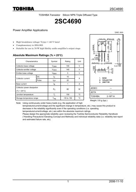
<strong>2SC4690</strong><br />
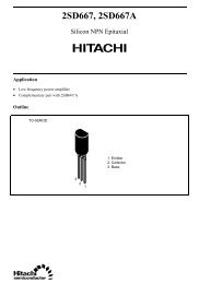
TOSHIBA Transistor Silicon NPN Triple Diffused Type<br />
<strong>2SC4690</strong><br />
Power Amplifier Applications<br />
Unit: mm<br />
• High breakdown voltage: V CEO = 140 V (min)<br />
• Complementary to 2SA1805<br />
• Suitable for use in 70-W high fidelity <strong>audio</strong> amplifier’s output <strong>stage</strong><br />
Absolute Maximum Ratings (Tc = 25°C)<br />
Characteristics Symbol Rating Unit<br />
Collector-base voltage V CBO 140 V<br />
Collector-emitter voltage V CEO 140 V<br />
Emitter-base voltage V EBO 5 V<br />
Collector current<br />
DC I C 10<br />
Pulse I CP 20<br />
Base current I B 1 A<br />
Collector power dissipation<br />
(Tc = 25°C)<br />
P C 80 W<br />
Junction temperature T j 150 °C<br />
TOSHIBA 2-16F1A<br />
Storage temperature range T stg −55 to 150 °C<br />
Weight: 5.8 g (typ.)<br />
Note: Using continuously under heavy loads (e.g. the application of high<br />
temperature/current/voltage and the significant change in temperature, etc.) may cause this product to<br />
decrease in the reliability significantly even if the operating conditions (i.e. operating<br />
temperature/current/voltage, etc.) are within the absolute maximum ratings.<br />
Please design the appropriate reliability upon reviewing the Toshiba Semiconductor Reliability Handbook<br />
(“Handling Precautions”/Derating Concept and Methods) and individual reliability data (i.e. reliability test report<br />
and estimated failure rate, etc).<br />
A<br />
JEDEC<br />
JEITA<br />
―<br />
―<br />
1<br />
2006-11-10
<strong>2SC4690</strong><br />
Electrical Characteristics (Tc = 25°C)<br />
Characteristics Symbol Test Condition Min Typ. Max Unit<br />
Collector cut-off current I CBO V CB = 140 V, I E = 0 ― ― 5.0 μA<br />
Emitter cut-off current I EBO V EB = 5 V, I C = 0 ― ― 5.0 μA<br />
Collector-emitter breakdown voltage V (BR) CEO I C = 50 mA, I B = 0 140 ― ― V<br />
DC current gain<br />
h FE (1)<br />
(Note)<br />
V CE = 5 V, I C = 1 A 55 ― 160<br />
h FE (2) V CE = 5 V, I C = 5 A 35 85 ―<br />
Collector-emitter saturation voltage V CE (sat) I C = 7 A, I B = 0.7 A ― 0.3 2.0 V<br />
Base-emitter voltage V BE V CE = 5 V, I C = 5 A ― 0.9 1.5 V<br />
Transition frequency f T V CE = 5 V, I C = 1 A ― 30 ― MHz<br />
Collector output capacitance C ob V CB = 10 V, I E = 0, f = 1 MHz ― 220 ― pF<br />
Note: h FE (1) classification R: 55 to 110, O: 80 to 160<br />
Marking<br />
C4690<br />
Part No. (or abbreviation code)<br />
Lot No.<br />
Characteristics<br />
indicator<br />
A line indicates<br />
lead (Pb)-free package or<br />
lead (Pb)-free finish.<br />
2<br />
2006-11-10
<strong>2SC4690</strong><br />
Collector current IC (A)<br />
10<br />
8<br />
6<br />
4<br />
2<br />
500<br />
300<br />
I C – V CE<br />
200<br />
20<br />
IB = 10 mA<br />
150<br />
100<br />
70<br />
50<br />
30<br />
Common emitter<br />
Tc = 25°C<br />
Collector current IC (A)<br />
10<br />
8<br />
6<br />
4<br />
2<br />
Tc = 100°C<br />
25<br />
−25<br />
I C – V BE<br />
Common emitter<br />
VCE = 5 V<br />
0<br />
0<br />
2 4 6 8 10 12<br />
0<br />
0<br />
0.4 0.8 1.2 1.6 2.0 2.4<br />
Collector-emitter voltage V CE (V)<br />
Base-emitter voltage V BE (V)<br />
DC current gain hFE<br />
1000<br />
500<br />
300<br />
100<br />
50<br />
30<br />
10<br />
5<br />
0.01<br />
h FE – I C<br />
Common emitter<br />
VCE = 5 V<br />
Tc = 100°C<br />
25<br />
−25<br />
0.03 0.1 0.3 1 3 10<br />
Collector-emitter saturation voltage<br />
VCE (sat) (V)<br />
2<br />
1<br />
0.5<br />
0.3<br />
0.1<br />
0.05<br />
0.03<br />
0.01<br />
0.01<br />
Tc = −25°C<br />
25<br />
100<br />
V CE (sat) – I C<br />
Common emitter<br />
IC/IB = 10<br />
0.03 0.1 0.3 1 3 10<br />
Collector current I C (A)<br />
Collector current I C (A)<br />
Transition frequency fT (MHz)<br />
200<br />
100<br />
50<br />
30<br />
10<br />
5<br />
3<br />
1<br />
0.01<br />
f T – I C<br />
Common emitter<br />
Tc = 25°C<br />
VCE = 5 V<br />
0.03 0.1 0.3 1 3 10<br />
Collector current IC (A)<br />
50<br />
30<br />
10<br />
5<br />
3<br />
IC max (pulsed)*<br />
IC max (continuous)<br />
Safe Operating Area<br />
DC operation<br />
(Tc = 25°C)<br />
100 ms*<br />
1 ms*<br />
10 ms*<br />
1<br />
0.5<br />
*: Single nonrepetitive pulse<br />
Tc = 25°C<br />
0.3<br />
Curves must be derated linearly<br />
with increase in temperature.<br />
VCEO<br />
max<br />
0.1<br />
0.3 1 3 10 30 100 300<br />
Collector current I C (A)<br />
Collector-emitter voltage V CE (V)<br />
3<br />
2006-11-10
<strong>2SC4690</strong><br />
RESTRICTIONS ON PRODUCT USE<br />
20070701-EN<br />
• The information contained herein is subject to change without notice.<br />
• TOSHIBA is continually working to improve the quality and reliability of its products. Nevertheless, semiconductor<br />
devices in general can malfunction or fail due to their inherent electrical sensitivity and vulnerability to physical<br />
stress. It is the responsibility of the buyer, when utilizing TOSHIBA products, to comply with the standards of<br />
safety in making a safe design for the entire system, and to avoid situations in which a malfunction or failure of<br />
such TOSHIBA products could cause loss of human life, bodily injury or damage to property.<br />
In developing your designs, please ensure that TOSHIBA products are used within specified operating ranges as<br />
set forth in the most recent TOSHIBA products specifications. Also, please keep in mind the precautions and<br />
conditions set forth in the “Handling Guide for Semiconductor Devices,” or “TOSHIBA Semiconductor Reliability<br />
Handbook” etc.<br />
• The TOSHIBA products listed in this document are intended for usage in general electronics applications<br />
(computer, personal equipment, office equipment, measuring equipment, industrial robotics, domestic appliances,<br />
etc.).These TOSHIBA products are neither intended nor warranted for usage in equipment that requires<br />
extraordinarily high quality and/or reliability or a malfunction or failure of which may cause loss of human life or<br />
bodily injury (“Unintended Usage”). Unintended Usage include atomic energy control instruments, airplane or<br />
spaceship instruments, transportation instruments, traffic signal instruments, combustion control instruments,<br />
medical instruments, all types of safety devices, etc.. Unintended Usage of TOSHIBA products listed in his<br />
document shall be made at the customer’s own risk.<br />
• The products described in this document shall not be used or embedded to any downstream products of which<br />
manufacture, use and/or sale are prohibited under any applicable laws and regulations.<br />
• The information contained herein is presented only as a guide for the applications of our products. No<br />
responsibility is assumed by TOSHIBA for any infringements of patents or other rights of the third parties which<br />
may result from its use. No license is granted by implication or otherwise under any patents or other rights of<br />
TOSHIBA or the third parties.<br />
• Please contact your sales representative for product-by-product details in this document regarding RoHS<br />
compatibility. Please use these products in this document in compliance with all applicable laws and regulations<br />
that regulate the inclusion or use of controlled substances. Toshiba assumes no liability for damage or losses<br />
occurring as a result of noncompliance with applicable laws and regulations.<br />
4<br />
2006-11-10


![Mark Levinson JC-1DC_ckt[1].](https://img.yumpu.com/30568679/1/190x135/mark-levinson-jc-1dc-ckt1.jpg?quality=85)