Motorola PNP Silicon Transistor 2N4033 - West Florida Components
Motorola PNP Silicon Transistor 2N4033 - West Florida Components
Motorola PNP Silicon Transistor 2N4033 - West Florida Components

Create successful ePaper yourself
Turn your PDF publications into a flip-book with our unique Google optimized e-Paper software.
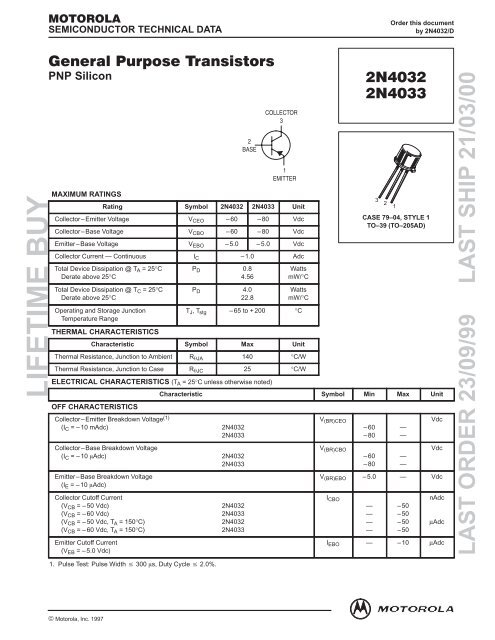
SEMICONDUCTOR TECHNICAL DATAOrder this documentby 2N4032/DLIFETIME BUY <strong>PNP</strong> <strong>Silicon</strong>MAXIMUM RATINGSRating Symbol 2N4032 <strong>2N4033</strong> UnitCollector–Emitter Voltage V CEO –60 –80 VdcCollector–Base Voltage V CBO –60 –80 VdcEmitter–Base Voltage V EBO –5.0 –5.0 VdcCollector Current — Continuous I C –1.0 AdcTotal Device Dissipation @ T A = 25°CDerate above 25°CTotal Device Dissipation @ T C = 25°CDerate above 25°COperating and Storage JunctionTemperature RangeTHERMAL CHARACTERISTICSP D 0.84.56P D 4.022.8WattsmW/°CWattsmW/°CT J , T stg –65 to + 200 °CCharacteristic Symbol Max UnitThermal Resistance, Junction to Ambient R JA 140 °C/WThermal Resistance, Junction to Case R JC 25 °C/WELECTRICAL CHARACTERISTICS (T A = 25°C unless otherwise noted)Characteristic Symbol Min Max UnitOFF CHARACTERISTICSCollector–Emitter Breakdown Voltage (1)(I C = – 10 mAdc) 2N4032<strong>2N4033</strong>Collector–Base Breakdown Voltage(I C = – 10 Adc) 2N4032<strong>2N4033</strong>Emitter–Base Breakdown Voltage(I E = – 10 Adc)Collector Cutoff Current(V CB = – 50 Vdc) 2N4032(V CB = – 60 Vdc) <strong>2N4033</strong>(V CB = – 50 Vdc, T A = 150°C) 2N4032(V CB = – 60 Vdc, T A = 150°C) <strong>2N4033</strong>Emitter Cutoff Current(V EB = – 5.0 Vdc)1. Pulse Test: Pulse Width 300 s, Duty Cycle 2.0%.2BASECOLLECTOR31EMITTERV (BR)CEO–60–80V (BR)CBO–60–80————VdcVdcV (BR)EBO –5.0 — VdcI CBO————32CASE 79–04, STYLE 1TO–39 (TO–205AD)–50–50–50–50nAdcµAdcI EBO — –10 µAdc1LAST ORDER 23/09/99 LAST SHIP 21/03/00<strong>Motorola</strong> Small–Signal <strong>Transistor</strong>s, FETs and Diodes Device Data© <strong>Motorola</strong>, Inc. 19971
ELECTRICAL CHARACTERISTICS (T A = 25°C unless otherwise noted) (Continued)LIFETIME BUYCharacteristic Symbol Min Max UnitON CHARACTERISTICSDC Current Gainh FE —(I C = – 100 mAdc, V CE = – 5.0 Vdc, @ – 55°C) (1) 2N4032,3340 —(I C = – 100 µAdc, V CE = – 5.0 Vdc) 2N4032,33(I C = – 100 mAdc, V CE = – 5.0 Vdc) (1) 2N4032,33(I C = – 500 mAdc, V CE = – 5.0 Vdc) (1) 2N4032,33(I C = – 1.0 Adc, V CE = – 5.0 Vdc) (1) 2N4032<strong>2N4033</strong>Collector–Emitter Saturation Voltage (1)(I C = – 150 mAdc, I B = – 15 mAdc)(I C = – 500 mAdc, I B = – 50 mAdc)(I C = – 1.0 Adc, I B = – 100 mAdc) 2N4032Base–Emitter Saturation Voltage (1)(I C = – 150 mAdc, I B = – 15 mAdc)75100704025V CE(sat)———Base–Emitter On VoltageV BE(on)(I C = –1.0 Adc, V CE = –1.0 Vdc) 2N4032—(I C = – 500 mAdc, V CE = – 0.5 Vdc) (1) —SMALL–SIGNAL CHARACTERISTICSOutput Capacitance(V CE = –10 Vdc, f = 1.0 MHz)Input Capacitance(V EB = – 0.5 Vdc, f = 1.0 MHz)Small Signal Current Gain(I C = – 50 mAdc, V CE = –10 Vdc, f = 100 MHz)SWITCHING CHARACTERISTICSStorage Time(I C = – 500 mAdc, I B1 = I B2 = – 50 mAdc)Turn–On Time(I C = – 500 mAdc, I B1 = – 50 mAdc)Fall Time(I C = – 500 mAdc, I B1 = I B2 = – 50 mAdc)1. Pulse Test: Pulse Width 300 s, Duty Cycle 2.0%.—300———–0.15–0.5–1.0VdcV BE(sat) — –0.9 Vdc–1.2–1.1VdcC obo — 20 pFC ibo — 110 pFh fe 1.5 5.0 —t s — 350 nst on — 100 nst f — 50 nsLAST ORDER 23/09/99 LAST SHIP 21/03/002 <strong>Motorola</strong> Small–Signal <strong>Transistor</strong>s, FETs and Diodes Device Data
SWITCHING TIME EQUIVALENT TEST CIRCUITSLIFETIME BUYCAPACITANCE (pF)t, TIME (ns)100503020105.03.02.0+ 2.0 V0–10.85 VPULSE WIDTH = 200 nsRISE TIME ≤ 2.0 nsDUTY CYCLE ≤ 2.0%R CSCOPE200 ΩR BFigure 1. Turn–On– 30 VREVERSE VOLTAGE (VOLTS)Figure 3. Capacitances59 Ω1.0– 0.1 – 0.2 – 0.3 – 0.5 – 1.0 – 2.0 – 3.0 – 5.0 – 10 – 20– 30 – 50 – 10010070503020107.05.0–10V BE(off) = 0 VC ebI C /I B = 10V BE(off) = 2.0 VFigure 5. Delay TimeQ, CHARGE (nC)011.2 V+ 8.8 Vt 1t 2t 3TRANSIENT CHARACTERISTICS25°C 100°CC cbt, TIME (ns)107.05.03.02.01.00.70.50.30.2V CC = – 30 VI C /I B = 102 < t 1 < 500 µs2 < t 2 < 5.0 ns2 < t 3 > 1.0 µsDUTY CYCLE = 2.0%200 ΩR B1N916+ 3.0 VFigure 2. Turn–OffQ T– 30 VR CI C , COLLECTOR CURRENT (mA)Figure 4. Charge DataQ A59 ΩSCOPE0.1– 10 – 20 – 30 – 50 – 100 – 200 – 300 – 500 – 100010070503020107.05.0– 20 – 30 – 50 – 70 – 100 – 200 – 300 – 500 – 700 – 1000 – 10 – 20 – 30 – 50 – 70 – 100 – 200 – 300 – 500 – 700 – 1000I C , COLLECTOR CURRENT (mA)I C , COLLECTOR CURRENT (mA)Figure 6. Rise TimeV CC = – 30 VI C /I B = 10LAST ORDER 23/09/99 LAST SHIP 21/03/00<strong>Motorola</strong> Small–Signal <strong>Transistor</strong>s, FETs and Diodes Device Data3
f t , STORAGE TIME (ns)sLIFETIME BUYNF, NOISE FIGURE (dB)h fe , CURRENT GAIN10007005003002001007050302010–10109.08.07.06.05.04.03.02.01.0I C , COLLECTOR CURRENT (mA)Figure 7. Storage TimeI C = –1.0 mA, R S = 100I B1 = I B2I C /I B = 10V CC = – 30 Vt s ′ = t s – 1/3 t f00.01 0.02 0.03 0.05 0.1 0.2 0.3 0.5 1.0 2.0 3.0 5.0 10f, FREQUENCY (kHz)300200100705030– 20 – 30 – 50 – 70 – 100 – 200 – 300 – 500 – 700 – 1000–100 µA, R S = 680–10 µA, R S = 7.0 kΩFigure 9. Frequency EffectsI C , COLLECTOR CURRENT (mA)t , FALL TIME (ns)200SMALL–SIGNAL CHARACTERISTICSNOISE FIGUREV CE = 10 Vdc, T A = 25°CR S = OPTIMUM SOURCE RESISTANCENF, NOISE FIGURE (dB)1007050h PARAMETERSV CE = 10 Vdc, f = 1.0 kHz, T A = 25°C3020I C , COLLECTOR CURRENT (mA)Figure 8. Fall Time–10 AR S , SOURCE RESISTANCE (OHMS)V CC = – 30 VI C /I B = 10I B1 = I B210– 10 – 20 – 30 – 50 – 70 – 100 – 200 – 300 – 500 – 700 – 1000109.08.07.06.05.04.03.0–100 A2.01.0 I C = –1.0 mAf = 1.0 kHz050 100 200 300 500 1.0k 2.0k 3.0k 5.0k 10k 20k 30k 50kFigure 10. Source Resistance EffectsThis group of graphs illustrates the relationship of the “h” parameters for this series of transistors. To obtain thesecurves, 4 units were selected and identified by number - the same units were used to develop curves on each graph.UNIT 43212015– 0.1 – 0.2 – 0.3 – 0.5 – 1.0 – 2.0 – 3.0 – 5.0 – 10h ie , INPUT IMPEDANCE (k OHMS)3020107.05.03.02.01.00.70.5UNIT 12430.3– 0.1 – 0.2 – 0.3 – 0.5 – 1.0 – 2.0 – 3.0 – 5.0 – 10I C , COLLECTOR CURRENT (mA)LAST ORDER 23/09/99 LAST SHIP 21/03/00Figure 11. Current GainFigure 12. Input Impedance4 <strong>Motorola</strong> Small–Signal <strong>Transistor</strong>s, FETs and Diodes Device Data
h , VOLTAGE FEEDBACK RATIO (X 10 –4re)LIFETIME BUYhFE, DC CURRENT GAIN (NORMALIZED)1007050VCE, COLLECTOR–EMITTER VOLTAGE (VOLTS)3020107.05.03.02.0324UNIT 11.0– 0.1 – 0.2 – 0.3 – 0.5 – 1.0 – 2.0 – 3.0 – 5.0 – 10107.05.03.02.01.00.70.50.30.2I C , COLLECTOR CURRENT (mA)Figure 13. Voltage Feedback RatioT J = 175°C25°C –55°Ch oe , OUTPUT ADMITTANCE ( mhos)STATIC CHARACTERISTICS432UNIT 11.0– 0.1 – 0.2 – 0.3 – 0.5 – 1.0 – 2.0 – 3.0 – 5.0 – 10I C , COLLECTOR CURRENT (mA)Figure 14. Output AdmittanceV CE = –1.0 VV CE = –10 V0.1– 1.0 – 2.0 – 3.0 – 5.0 – 7.0 – 10 – 20 – 30 – 50 – 70 – 100 – 200 – 300 – 500 – 700 – 1000I C , COLLECTOR CURRENT (mA)– 1.0– 0.8– 0.6– 0.4– 0.2I C = – 1.0 mA– 10 mAFigure 15. DC Current Gain0– 0.005 – 0.007 – 0.01 – 0.02 – 0.03 – 0.05 – 0.07 – 0.1 – 0.2 – 0.3 – 0.5 – 0.7 – 1.0 – 2.0 – 3.0 – 5.0 – 7.0 – 10 – 20 – 30 – 50I B , BASE CURRENT (mA)1007050107.05.03.02.0Figure 16. Collector Saturation Region3020– 100 mA– 500 mAT J = 25°CLAST ORDER 23/09/99 LAST SHIP 21/03/00<strong>Motorola</strong> Small–Signal <strong>Transistor</strong>s, FETs and Diodes Device Data5
–1.0+1.0VOLTAGE (VOLTS)LIFETIME BUYIC, COLLECTOR CURRENT (AMP)– 0.8– 0.6– 0.4– 0.2V BE(sat) @ I C /I B = 10V CE(sat) @ I C /I B = 100– 1.0 – 2.0 – 3.0 – 5.0 –10 –20 – 30 – 50 – 100 – 200– 300 – 500 – 1000– 3.0– 2.0– 1.0– 0.5– 0.3– 0.2– 0.1– 0.07– 0.05– 0.03– 1.0V BE(on) @ V CE = –1.0 VI C , COLLECTOR CURRENT (mA)Figure 17. “On” VoltagesT J = 200°CSECONDARY BREAKDOWNLIMITEDBONDING WIRE LIMITEDTHERMALLY LIMITEDT C = 25°C (SINGLE PULSE)CURVES APPLY BELOWRATED V CEO1.0 msV CE , COLLECTOR–EMITTER VOLTAGE (VOLTS)COEFFICIENT (mV/ ° C)– 1.0– 2.0RATINGS AND THERMAL DATA– 2.0 – 3.0 – 5.0 – 7.0 –10 –20 – 30 – 50 – 70 – 100dc0.1 msFigure 19. Safe Operating Area0– 3.0θ VC for V CE(sat)θ VB for V BE– 4.0– 1.0 – 2.0 – 3.0 – 5.0 –10 –20 – 30 – 50 – 100 – 200 – 300 – 500 – 1000I C , COLLECTOR CURRENT (mA)Figure 18. Temperature CoefficientsThe safe operating area curves indicate I C –V CE limits of thetransistor that must be observed for reliable operation. Collectorload lines for specific circuits must fall below the limits indicated bythe applicable curve.The data of Figure 19 is based upon T J(pk) = 200°C; T C is variabledepending upon conditions. Pulse curves are valid for duty cyclesto 10% provided T J(pk) ≤ 200°C. T J(pk) may be calculated from thedata in Figure 20. At high case temperatures, thermal limitations willreduce the power that can be handled to values less than thelimitations imposed by second breakdown.LAST ORDER 23/09/99 LAST SHIP 21/03/006 <strong>Motorola</strong> Small–Signal <strong>Transistor</strong>s, FETs and Diodes Device Data
PACKAGE DIMENSIONSLIFETIME BUY–T–RE–H–MFJ1B2P–A–LCKSEATINGPLANED 3 PL0.36 (0.014) M T A M H M3GSTYLE 1:PIN 1. EMITTER2. BASE3. COLLECTORCASE 079–04(TO–205AD)ISSUE NNOTES:1. DIMENSIONING AND TOLERANCING PER ANSIY14.5M, 1982.2. CONTROLLING DIMENSION: INCH.3. DIMENSION J MEASURED FROM DIMENSION AMAXIMUM.4. DIMENSION B SHALL NOT VARY MORE THAN0.25 (0.010) IN ZONE R. THIS ZONECONTROLLED FOR AUTOMATIC HANDLING.5. DIMENSION F APPLIES BETWEEN DIMENSIONP AND L. DIMENSION D APPLIES BETWEENDIMENSION L AND K MINIMUM. LEADDIAMETER IS UNCONTROLLED IN DIMENSIONP AND BEYOND DIMENSION K MINIMUM.INCHES MILLIMETERSDIM MIN MAX MIN MAXA 0.335 0.370 8.51 9.39B 0.305 0.335 7.75 8.50C 0.240 0.260 6.10 6.60D 0.016 0.021 0.41 0.53E 0.009 0.041 0.23 1.04F 0.016 0.019 0.41 0.48G 0.200 BSC 5.08 BSCH 0.028 0.034 0.72 0.86J 0.029 0.045 0.74 1.14K 0.500 0.750 12.70 19.05L 0.250 ––– 6.35 –––M 45 BSC 45 BSCP ––– 0.050 ––– 1.27R 0.100 ––– 2.54 –––LAST ORDER 23/09/99 LAST SHIP 21/03/00<strong>Motorola</strong> Small–Signal <strong>Transistor</strong>s, FETs and Diodes Device Data7
LIFETIME BUY<strong>Motorola</strong> reserves the right to make changes without further notice to any products herein. <strong>Motorola</strong> makes no warranty, representation or guarantee regardingthe suitability of its products for any particular purpose, nor does <strong>Motorola</strong> assume any liability arising out of the application or use of any product or circuit, andspecifically disclaims any and all liability, including without limitation consequential or incidental damages. “Typical” parameters which may be provided in <strong>Motorola</strong>data sheets and/or specifications can and do vary in different applications and actual performance may vary over time. All operating parameters, including “Typicals”must be validated for each customer application by customer’s technical experts. <strong>Motorola</strong> does not convey any license under its patent rights nor the rights ofothers. <strong>Motorola</strong> products are not designed, intended, or authorized for use as components in systems intended for surgical implant into the body, or otherapplications intended to support or sustain life, or for any other application in which the failure of the <strong>Motorola</strong> product could create a situation where personal injuryor death may occur. Should Buyer purchase or use <strong>Motorola</strong> products for any such unintended or unauthorized application, Buyer shall indemnify and hold <strong>Motorola</strong>and its officers, employees, subsidiaries, affiliates, and distributors harmless against all claims, costs, damages, and expenses, and reasonable attorney feesarising out of, directly or indirectly, any claim of personal injury or death associated with such unintended or unauthorized use, even if such claim alleges that<strong>Motorola</strong> was negligent regarding the design or manufacture of the part. <strong>Motorola</strong> and are registered trademarks of <strong>Motorola</strong>, Inc. <strong>Motorola</strong>, Inc. is an EqualOpportunity/Affirmative Action Employer.Mfax is a trademark of <strong>Motorola</strong>, Inc.How to reach us:USA / EUROPE / Locations Not Listed: <strong>Motorola</strong> Literature Distribution; JAPAN: Nippon <strong>Motorola</strong> Ltd.; Tatsumi–SPD–JLDC, 6F Seibu–Butsuryu–Center,P.O. Box 5405, Denver, Colorado 80217. 303–675–2140 or 1–800–441–2447 3–14–2 Tatsumi Koto–Ku, Tokyo 135, Japan. 81–3–3521–8315LAST ORDER 23/09/99 LAST SHIP 21/03/00Mfax: RMFAX0@email.sps.mot.com – TOUCHTONE 602–244–6609 ASIA/PACIFIC: <strong>Motorola</strong> Semiconductors H.K. Ltd.; 8B Tai Ping Industrial Park,– US & Canada ONLY 1–800–774–1848 51 Ting Kok Road, Tai Po, N.T., Hong Kong. 852–26629298INTERNET: http://motorola.com/sps8 ◊<strong>Motorola</strong> Small–Signal <strong>Transistor</strong>s, FETs and Diodes Device 2N4032/D Data

![Mark Levinson JC-1DC_ckt[1].](https://img.yumpu.com/30568679/1/190x135/mark-levinson-jc-1dc-ckt1.jpg?quality=85)