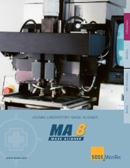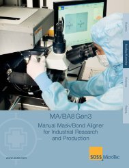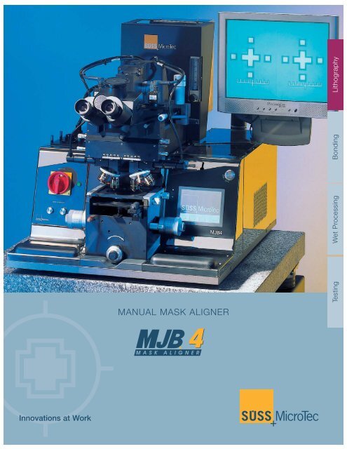
MANUAL MASK ALIGNER
MANUAL MASK ALIGNER
MANUAL MASK ALIGNER

You also want an ePaper? Increase the reach of your titles
YUMPU automatically turns print PDFs into web optimized ePapers that Google loves.
Testing Wet Processing Bonding<br />
Lithography<br />
<strong>MANUAL</strong> <strong>MASK</strong> <strong>ALIGNER</strong><br />
Innovations at Work
Contents<br />
Introduction . . . . . . . . . . . . . . . . . . . . . . . . . . . . . . . . . . . . . . . . . . . . . . . . . . . . . . . . . . . . . . . . . . . . . . P. 2<br />
Printing Modes . . . . . . . . . . . . . . . . . . . . . . . . . . . . . . . . . . . . . . . . . . . . . . . . . . . . . . . . . . . . . . . . . . . . P. 3<br />
Exposure System . . . . . . . . . . . . . . . . . . . . . . . . . . . . . . . . . . . . . . . . . . . . . . . . . . . . . . . . . . . . . . . . . . P. 4<br />
Exposure Optics . . . . . . . . . . . . . . . . . . . . . . . . . . . . . . . . . . . . . . . . . . . . . . . . . . . . . . . . . . . . . . . . . . . P. 5<br />
Alignment Stage . . . . . . . . . . . . . . . . . . . . . . . . . . . . . . . . . . . . . . . . . . . . . . . . . . . . . . . . . . . . . . . . . . . P. 6<br />
Manual Optical Alignment . . . . . . . . . . . . . . . . . . . . . . . . . . . . . . . . . . . . . . . . . . . . . . . . . . . . . . . . . . . . P. 7<br />
Microscopes . . . . . . . . . . . . . . . . . . . . . . . . . . . . . . . . . . . . . . . . . . . . . . . . . . . . . . . . . . . . . . . . . . . . . . P. 8<br />
SUSS IR-Systems . . . . . . . . . . . . . . . . . . . . . . . . . . . . . . . . . . . . . . . . . . . . . . . . . . . . . . . . . . . . . . . . . . P. 9<br />
MJB4 Configurations . . . . . . . . . . . . . . . . . . . . . . . . . . . . . . . . . . . . . . . . . . . . . . . . . . . . . . . . . . . . . . . . P. 10<br />
Technical Data . . . . . . . . . . . . . . . . . . . . . . . . . . . . . . . . . . . . . . . . . . . . . . . . . . . . . . . . . . . . . . . . . . . . P. 10–11<br />
Features and benefits<br />
MJB4<br />
Mask Aligner<br />
The MJB4 design is based on the highly acclaimed<br />
MJB3, which set standards for precision, reliability<br />
and high performance. Since its release in 1969 more<br />
than 2000 machines have been installed worldwide.<br />
The MJB4 is the next manual mask aligner following<br />
the MJB3. It is the ideal, economical tool for laboratories<br />
and small series production. In its contact exposure<br />
modes, the equipment can achieve a resolution<br />
of 0.5 µm, a performance unsurpassed in any other<br />
comparable machine.<br />
■ High resolution printing down to 0.5 µm<br />
■<br />
■<br />
■<br />
■<br />
■<br />
■<br />
■<br />
■<br />
■<br />
Wafer and substrate handling up to<br />
100 mm (wafers), 44 (substrates)<br />
Special substrate chucks for pieces,<br />
III-V materials, thick substrates, hybrids<br />
and HF components<br />
High precision X, Y, alignment stage<br />
and microscope manipulator<br />
High intensity optical configurations<br />
for different UV-exposure wavelengths<br />
up to 80 mW/cm 2<br />
Minimum operator training<br />
Ergonomic operation<br />
Touch panel graphical user interface<br />
Easy access to all assemblies of the mask<br />
aligner<br />
Laser applications on request<br />
The machine is widely used for MEMS and optoelectronics<br />
applications. It is specially configured<br />
for handling nonstandard substrates such as hybrids,<br />
high-frequency components or fragile III-V materials,<br />
such as GaAs or InP.<br />
The tool can be equipped with either a SUSS Singlefield<br />
or a Splitfield microscope enabling fast and highly accurate<br />
alignment.<br />
Introduction<br />
2
Printing Modes<br />
MJB4 Resolution<br />
Resolution UV400 UV300 UV250<br />
Soft Contact 2.0 µm < 2.0 µm –<br />
Hard Contact 1.0 µm < 1.0 µm –<br />
Vacuum Contact < 0.8 µm < 0.6 µm < 0.5 µm<br />
Gap Exposure > 3.0 µm<br />
Lithography<br />
Resolution achieved in 1 µm thick resist (AZ5214E), lines & spaces<br />
Achievable resolution depends on wafer size, wafer flatness, resist type,<br />
clean room condition and therefore, might vary for different processes.<br />
The MJB4 is capable of handling several exposure<br />
sequences:<br />
Soft Contact<br />
In its soft contact exposure mode the MJB4 can<br />
achieve a resolution of 2.0 µm. The final data mainly<br />
depends on process specifications such as spectral<br />
range, the distance between mask and wafer, a function<br />
of wafer topography, cleanliness and exposure<br />
mode, as well as diffraction reduction.<br />
Low Vacuum Contact<br />
For brittle or fragile substrates a low vacuum contact<br />
exposure can be performed. The low vacuum contact<br />
exposure mode reduces the vacuum impact to the<br />
substrate. This feature enables for a better resolution<br />
not achievable in soft or hard contact.<br />
Hard Contact<br />
With the hard contact exposure mode the gap between<br />
mask and wafer is further reduced by purging<br />
nitrogen underneath the wafer. Thus the wafer is<br />
pushed harder against the mask and achieves a<br />
resolution in the 1 micron range.<br />
Gap Printing<br />
Although the MJB4 is not considered to be a proximity<br />
exposure system, the gap printing mode allows exposure<br />
at a pre-set gap of up to 50 µm after initial wafer<br />
to mask leveling. This reduces mask wear for larger<br />
feature sizes.<br />
Vacuum Contact<br />
The MJB4 can perform vacuum contact processes<br />
achieving a resolution in submicron range. Vacuum contact<br />
yields considerably higher resolution than hard or<br />
soft contact, because the gap between mask and wafer<br />
is further reduced. To obtain the highest resolution the<br />
photoresist thickness also needs to be optimized.<br />
The SUSS Mask Pellicle Technology (MPT) option<br />
reduces the need for mask cleaning in both proximity<br />
and contact printing modes (for more information refer<br />
to the MPT sales bulletin).<br />
Soft Contact Hard Contact Vacuum Contact<br />
Printing Modes<br />
3
Conventional<br />
Mirror<br />
Light sensor<br />
Twin shutter<br />
Ellipsoidal mirror<br />
Cold light mirror<br />
Heat sink<br />
SUSS Optics<br />
Front lens/mask/wafer<br />
Condenser lens<br />
Diffraction red. optics<br />
Optical system of MJB4 mask aligner<br />
Exposure System<br />
High Quality Exposure Optics<br />
Strong diffraction effects from parallel<br />
illumination (upper graphic) vs. SUSS<br />
diffraction reducing optics (shown below).<br />
SUSS MicroTec is the only semiconductor<br />
equipment supplier offering diffraction<br />
reducing optical setups.<br />
SUSS offers a variety of optical configurations designed<br />
to compensate diffraction effects for various<br />
spectral ranges. Diffractions are a significant factor<br />
in the improvement of resolution and yield optimum<br />
resist sidewall slopes.<br />
Diffraction effects at the mask pattern edges limit the<br />
achievable resolution. They are proportional to the<br />
square roof of the wavelength. Therefore shorter wavelengths<br />
provide less diffraction. SUSS diffraction reducing<br />
exposure optics are available for the spectral ranges<br />
UV400, UV300 and UV250. All MJB4 configurations<br />
incorporate the diffraction reducing SUSS optical<br />
system, individually optimized for the particular spectral<br />
region and the corresponding desired resolution.<br />
MJB4 mask holder<br />
Spectral Ranges<br />
Exposure System<br />
Range Wavelength Range Exposure Lamps<br />
Near UV UV400 (350 – 450 nm) 200/350 W Hg<br />
Mid UV UV300 (280 – 350 nm) 200/350 W Hg<br />
Deep UV UV250 (240 – 260 nm) 500 W HgXe<br />
SUSS diffraction reducing exposure optics are incorporated in all MJB4 configurations.<br />
4
Lithography<br />
Intensity distribution in the various spectral regions. The intensity scale<br />
of the graphics varies, therefore the intensities may not be directly compared.<br />
Exposure Optics<br />
UV300/400 Standard Configuration<br />
The basic configuration of the MJB4 achieves its performance<br />
with the unfiltered spectrum of a 200 W<br />
high pressure mercury arc lamp and its associated<br />
exposure system with diffraction reduced light path.<br />
The MJB4 standard is an excellent, extremely versatile<br />
tool for R & D and laboratory applications.<br />
The 200 W lamp provides an intensity of around<br />
40 mW/cm 2 at broadband and 25 mW/cm 2 at i-line.<br />
The MJB4 exposure systems are manufactured from<br />
Herasil and are suitable for processes using near UV<br />
(UV400) or mid UV (UV300). Filter elements provide<br />
the different spectral ranges of g, h and i-line of the<br />
mercury spectrum.<br />
UV250 Submicron Configuration<br />
The UV250 exposure system incorporates Suprasil<br />
lenses for deep UV with corresponding light sources.<br />
For ozone removal the lamphouse can be optionally<br />
equipped with an exhaust and cooling system. SUSS<br />
recommends the exhaust system when working with<br />
DUV.<br />
For process techniques in the UV250 spectral range<br />
a suitable photoresist such as PMMA must be used.<br />
This resist is sensitive below 260 nm only.<br />
The Suprasil lens system can also be combined with<br />
the 200 W or 350 W Hg lamp and associated filter elements<br />
for processes in the UV400 or UV300 regions.<br />
Reliable submicron printing<br />
with SUSS diffraction<br />
reducing optics.<br />
(1 micron PMMA, UV250,<br />
vacuum contact)<br />
Exposure Optics<br />
5
Alignment Stage<br />
Precise alignment of mask and wafer is crucial for<br />
all lithography processes. Alignment is performed<br />
by moving the wafer, while keeping the mask stage<br />
stationary.<br />
XY Alignment Stage<br />
The MJB4 is equipped with a XY alignment stage<br />
using high precision, backlash-free micrometer spindles<br />
for X, Y and .<br />
The travel range for X and Y is ± 5 mm, for ± 5°.<br />
Substrate thickness compensation is easily adjustable<br />
allowing for a shift-free separation/contact movement.<br />
Alignment Stage<br />
The manual Z movement allows a maximum substrate<br />
thickness of up to 4 mm.<br />
The mechanically clamped mask holder is designed<br />
for quartz, glass or film masks. It is equipped with<br />
vacuum clamping for the mask. Mask holders and<br />
chucks are easily exchangeable. Existing MJB3<br />
equipment can be used on the MJB4 with a special<br />
mask holder frame.<br />
Fast and safe substrate loading/unloading is possible<br />
without removing mask holder or mask.<br />
Mask holder Mask Wafer<br />
Chuck Chuck stage Spindle<br />
Precise ball-bearing guide<br />
Pneumatic brake Leveling pistons<br />
WEC-System in the alignment stage. Soft contact<br />
for precise leveling. Inline vertical pneumatic clamping<br />
avoids any shifts.<br />
6
Lithography<br />
Standard topside alignment with M604 microscope<br />
Manual Optical Alignment<br />
Direct Alignment by Eye<br />
The human eye possesses a remarkable ability to<br />
recognize symmetry. The task to produce suitable<br />
alignment keys therefore consists of finding high contrast<br />
figures where symmetry can be recognized. A<br />
simple example is placing a small cross within a large<br />
cross. The line width of the large cross is not significant,<br />
if both sides of the cross can be observed.<br />
Mask targets<br />
For best alignment the gap between the edges of the<br />
small and the large crosses is critical. The minimum<br />
distance is approximately 2 µm. Typical values lie between<br />
3 and 5 µm, depending on contrast and edge<br />
quality. If the gap between the small and large alignment<br />
target is 3 µm, a misalignment of 0.5 µm causes<br />
a 40 percent intensity difference. SUSS has designed<br />
a range of alignment crosses meeting all important<br />
requirements.<br />
Misaligned mask<br />
and wafer targets<br />
Examples of 2 µm Misalignment<br />
Perfectly aligned<br />
targets<br />
20 µm<br />
Competition:<br />
Optical misperception by simple crosshair alignment<br />
(recognition of misalignment hardly possible)<br />
SUSS:<br />
The combination of microscopes with a large depth<br />
of focus (DOF) and a wide range of advanced alignment<br />
marks enables highest alignment accuracy<br />
(immediate recognition of misalignment)<br />
Features and benefits<br />
■<br />
■<br />
■<br />
■<br />
■<br />
Color image<br />
Large field of view<br />
Live-images, no risk of shift<br />
Cost effective<br />
Limited to depth of focus of respective<br />
objective<br />
Manual Optical Alignment<br />
7
Microscopes<br />
Microscope Manipulator<br />
The high alignment accuracy is obtained through the<br />
use of high resolution microscopes. In addition alignment<br />
accuracy can be checked before exposure in<br />
all exposure modes especially in vacuum contact.<br />
Standard topside alignment is performed with the<br />
M604 Splitfield microscope. Equipped with 10<br />
objectives it offers a simultaneous viewing of mask<br />
and wafer. For small substrate alignment the SUSS<br />
Singlefield microscope M500 might be a cost-effective<br />
solution. With both, the M604 and M500 an<br />
alignment accuracy of 1 µm or better is achievable.<br />
For manual alignment the full depth of focus of the<br />
microscope objectives is normally used. The line and<br />
space resolution is approximately 1 µm. It is not<br />
necessary to recognize submicron features in order<br />
to achieve submicron alignment accuracy.<br />
For fast microscope scanning of mask and wafer a<br />
microscope manipulator is standard. It is equipped<br />
with precise pneumatic brakes, vibration-, shift- and<br />
backlash-free positioning. A travel range of ± 40 mm<br />
in X, + 30 mm in Y, and – 50 mm allows for flat alignment<br />
of a four inch wafer / substrate.<br />
In case of working with a Singlefield microscope a<br />
fast X scanning movement is available. A rotation<br />
adjustment for the SUSS Splitfield microscope in<br />
a range of ± 4° is normal. Coarse and fine focus can<br />
be done with a conveniently combined control. An<br />
automatic microscope lift protects the high magnification<br />
objectives with short working distance, if the<br />
exposure cycle is initiated or if the mask has to be<br />
loaded or unloaded.<br />
The high alignment accuracy is obtained through<br />
the use of special 20 high resolution microscope<br />
objectives. They are optically compensated for<br />
observation through the mask.<br />
Microscope Options<br />
For demonstration and educational purposes both<br />
microscopes can be optionally equipped with CCD<br />
camera and monitor.<br />
M500 microscope<br />
M604 Splitfield Microscope<br />
Objective 2,5 5 10 20<br />
Resolution (µm) 4,2 2,2 1,1 0,9<br />
Depth of focus (µm) 195 51 13 4,5<br />
Field of view (mm) 4,65 2,33 1,16 0,58<br />
Magnification 47,3 94,6 189,2 378,3<br />
Microscopes<br />
8<br />
The MJB4 can be equipped<br />
with the M604 Splitfield<br />
microscope and the M500<br />
Singlefield microscope<br />
M500 Singlefield Microscope<br />
Objective 2,5 5 10 20<br />
Resolution (µm) 4,2 2,2 1,1 0,9<br />
Depth of focus (µm) 518 132 33 10<br />
Field of view (mm) 8,80 4,40 2,20 1,10<br />
Magnification 25 50 100 200
Lithography<br />
MJB4 Infrared Systems<br />
IR illumination unit<br />
For backside or buried layers feature alignment the<br />
SUSS MJB4 can be optionally equipped with an<br />
infrared system. There are two principles of IR alignment<br />
possible: The SUSS IR transmitted illumination<br />
system and the SUSS IR incident illumination system.<br />
Both are applicable to materials transparent to wavelengths<br />
in the range from 400 to 1200 nm. Both<br />
methods were incorporated for the handling of IR<br />
transparent materials like GaAs, InP, Silicon etc. Infrared<br />
alignment can also be used to align to buried<br />
diffusion layers.<br />
For IR alignment both microscopes, the M500 Singlefield<br />
and the M604 Splitfield, can be employed.<br />
Alignment Accuracy with IR<br />
Due to the specific design in most IR applications an<br />
alignment accuracy of ± 5 µm (± 2 µm under optimal<br />
process conditions) is achievable.<br />
SUSS IR Alignment System<br />
MJB4 standard chuck<br />
MJB4 IR chuck<br />
■<br />
■<br />
■<br />
■<br />
■<br />
■<br />
Infrared light source to be positioned<br />
manually<br />
Special IR chucks available<br />
One (M500) or two (M604) video<br />
cameras sensitive to wavelengths in<br />
the range from 400 to 1200 nm<br />
Video monitor<br />
Dedicated IR light source<br />
Dedicated IR objectives<br />
SUSS MicroTec Infrared Systems<br />
9
MJB4 Configurations<br />
The SUSS MJB4 submicron aligners are designed<br />
for the highest demands on resolution and alignment<br />
accuracy. They incorporate the highest SUSS quality<br />
in mechanics (alignment stage) and exposure optics.<br />
For specific applications SUSS offers optical set ups<br />
for UV250, UV300 and UV400.<br />
For Top Side / IR Alignment there are two microscopes<br />
available, the M500 Singlefield and the<br />
M604 Splitfield microscope.<br />
As a special advantage the MJB4 allows for an alignment<br />
check in all contact exposure modes.<br />
Exposure Lamp Power Supply<br />
There are three options available. Two standard<br />
power supplies for either the 200 W or the 350 W<br />
mercury lamp. Both are equipped with a smooth<br />
ignition system to prolong the lifetime of the lamp.<br />
The lamps operate at constant power only. The<br />
adjustment ranges are 150 W – 250 W (200 W Hg) or<br />
300 W – 430 W (350 W Hg).<br />
A more sophisticated power supply is the SUSS<br />
constant intensity controller (CIC 1200). It enables<br />
the operator to run lamps at constant intensity as<br />
well as in constant power. Each lamp can be adjusted<br />
to a specific intensity or power level. For<br />
UV 250 applications the CIC 1200 is mandatory.<br />
SUSS 604 Splitfield microscope<br />
with manipulator<br />
Technical Data<br />
Mask and Wafer / Substrate<br />
MJB4 Configurations/Technical Data<br />
10<br />
Substrate Size<br />
Wafer/Substrate Thickness<br />
Mask Size<br />
Mask Thickness<br />
Exposure System<br />
Lamp House<br />
1 up to 100 mm / 4 (round)<br />
55 mm up to 100100 mm / 44 (square)<br />
up to 4 mm<br />
22 up to 55<br />
up to 4.8 mm / 190 mil<br />
350 W<br />
Lamp Power<br />
200 W; 350 W; 500 W (DUV with HgXe lamp)<br />
Intensity 200 W 40 mW/cm 2 at 405 nm<br />
(average over 100 mm area)<br />
25 mW/cm 2 at 365 nm<br />
350 W 80 mW/cm 2 at 405 nm<br />
45 mW/cm 2 at 365 nm<br />
500 W 20 mW/cm 2 at 250 nm<br />
Uniformity 3%<br />
Spectrum<br />
UV400: 350 – 450 nm (g, h, i-line)<br />
UV300: 280 – 350 nm<br />
UV250: 240 – 260 nm
Print Resolution*<br />
UV400 UV300 UV250<br />
Soft Contact 2.0 µm < 2.0 µm –<br />
Hard Contact 1.0 µm < 1.0 µm –<br />
Vacuum Contact < 0.8 µm < 0.6 µm < 0.5 µm<br />
Gap Exposure > 3.0 µm<br />
* Lines and spaces; Resist AZ5214E, 1 µm, Wafer 100 mm<br />
Lithography<br />
Lamp Power Supply<br />
CPC (Standard)<br />
CIC1200<br />
Constant Power Controller for Hg200W or Hg350W<br />
Constant Intensity Controller for Hg200W, Hg350W and HgXe500W<br />
Alignment System<br />
Top Side Alignment<br />
IR Alignment<br />
M604 Illumination options<br />
M500 Singlefield microscope<br />
M604 Splitfield microscope<br />
Double Transmitted Illumination / M500 / one IR camera<br />
Single Incident Illumination / M500 / one IR camera<br />
Double Transmitted Illumination / M604 / two IR cameras<br />
Single Incident Illumination / M604 / two IR cameras<br />
Brightfield (standard); Dark Field; Interference contrast<br />
Topside Microscope Manipulator<br />
Travel Range X<br />
± 40 mm<br />
Travel Range Y<br />
+ 30 mm / – 50 mm<br />
Travel Range ±4°<br />
Alignment Stage<br />
Travel Range X<br />
± 5 mm<br />
Travel Range Y<br />
± 5 mm<br />
Travel Range ±5°<br />
Mechanical Resolution X, Y 0.1 µm<br />
Mechanical Resolution 410 –5°<br />
Utilities<br />
Vacuum Pressure<br />
< –0.8 bar (< 200 hPa absolute) / 150 mm or 6 Hg<br />
Vacuum Consumption<br />
0.25 m 3 /h (0.5 ft 3 /h)<br />
Compressed Dry Air Pressure > 5.5 bar (81 psi)<br />
Consumption 0.5 m 3 /h<br />
Nitrogen Pressure<br />
> 1.5 bar (22 psi)<br />
Nitrogen Consumption<br />
200 W lamp: 0.2 m 3 /h; 350 W lamp: 0.35 m 3 /h;<br />
500 W lamp: 0.7 m 3 /h<br />
Electrical Power Input<br />
95 V – 260 V, 50/60 Hz<br />
Consumption<br />
200 W lamp: 500 VA; 350 W lamp: 1650 VA;<br />
500 W lamp: 2250 VA<br />
Physical Dimensions<br />
WidthDepthHeight<br />
600800650 mm (243128)<br />
Footprint 0.5 m 2 (5 ft 2 )<br />
Weight<br />
up to 150 kg (331 pds)<br />
Data, design and specification of custom built machines depend on individual process conditions and can vary according<br />
to equipment configurations. Not all specifications may be valid simultaneously. Illustrations in this brochure are not<br />
legally binding. SUSS reserves the right to change machine specifications without prior notice.<br />
Technical Data<br />
11
ASIA<br />
SUSS MicroTec KK (Japan)<br />
GITC 1-18-2, Hakusan, Midori-ku<br />
Yokohama, Kanagawa, Japan 226-0006<br />
Phone (+81)-45-931-5600<br />
Fax (+81)-45-931-5601<br />
SUSS MicroTec (Shanghai) Co., Ltd.<br />
580 Nanjing W. Rd<br />
Nanzheng Building Room 606<br />
200041 Shanghai PRC<br />
Phone (+86) 21-52340432<br />
Fax (+86) 21-52340430<br />
SUSS MicroTec (Taiwan) Co., Ltd.<br />
8F-11 · No. 81 · Shui-Lee Road<br />
Hsin-Chu · 300 · Taiwan<br />
Phone (+886)-(3)-5169098<br />
Fax (+886)-(3)-5169262<br />
SUSS MicroTec Co., LTD (South and<br />
Northeast Asia)<br />
3388/92-93 · 25th Floor · Sirinrat Building<br />
Rama IV Road · Klongtoey<br />
Bangkok 10110 · Thailand<br />
Phone (+66)-(0)-2350 6038<br />
Fax (+66)-(0)-2633 5728<br />
EUROPE<br />
SUSS MicroTec Ltd.<br />
Unit 1 Scopwick Lodge Farm<br />
Scopwick Heath’<br />
Lincolnshire LN4 3DL · England<br />
Phone (+44)-(0) 1526-323147<br />
Fax (+44)-(0) 1526-322214<br />
SUSS MicroTec S.A.S.<br />
BP24 · 131 Impasse Barteudet<br />
F-74490 Saint Jeoire · France<br />
Phone (+33)-(0) 4 50 35 83 92<br />
Fax (+33)-(0) 4 50 35 88 01<br />
SUSS MicroTec Test Systems GmbH<br />
Süss-Strasse 1<br />
D-01561 Sacka/Dresden · Germany<br />
Phone (+49)-(0) 35240-73-0<br />
Fax (+49)-(0) 35240-73-700<br />
SUSS MicroTec Lithography GmbH<br />
Schleissheimer Strasse 90<br />
D-85748 Garching/Munich · Germany<br />
Phone (+49)-(0) 89/3 20 07-0<br />
Fax (+49)-(0) 89/3 20 07-162<br />
NORTH AMERICA<br />
SUSS MicroTec Inc.<br />
Western Regional Sales Office<br />
8240 So. Kyrene Road Suite 101<br />
Tempe, AZ 85284-2117 · USA<br />
Phone (+1) (480) 557-9370<br />
Fax (+1) (480) 557-9371<br />
SUSS MicroTec Inc.<br />
228 Suss Drive<br />
Waterbury Center, VT 05677 · USA<br />
Phone (+1) (802) 244-5181<br />
Fax (+1) (802) 244-5103<br />
JH/WM · 12/2004<br />
MJB4 · DE · 12/2004 · #1 · 2000<br />
www.suss.com