MA/BA8Gen3 - HILPERT electronics
MA/BA8Gen3 - HILPERT electronics
MA/BA8Gen3 - HILPERT electronics

You also want an ePaper? Increase the reach of your titles
YUMPU automatically turns print PDFs into web optimized ePapers that Google loves.
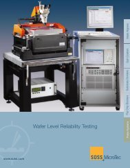
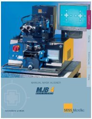
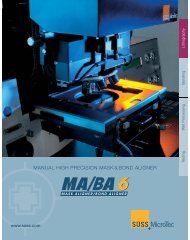
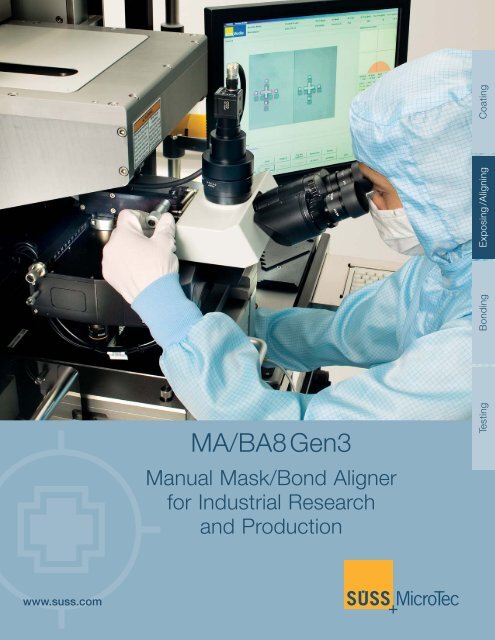
<strong>MA</strong>/<strong>BA8Gen3</strong>Manual Mask/Bond Alignerfor Industrial Researchand ProductionExposing /Aligning CoatingTesting Bonding Exposing /Aligningwww.suss.com
Breaking Technology BoundariesAn unmatched alignment precision coupled with high resolution andmaximum light uniformity makes the <strong>MA</strong>/BA8 the tool of choice fora variety of applications, ranging from MEMS, opto <strong>electronics</strong> and3D Packaging to micro-optics and nanotechnology.MEMSMicrofluidic deviceCourtesy: IMSAS, BremenUV LIGAMicro mechanical watch componentsCourtesy: Mimotec, SwitzerlandMEMSprinted in 500 µm SU8Courtesy: mrt, BerlinExposing /AligningCMOS Image Sensor Packaging,TSV LithographyVia top and bottom openingCourtesy: Schott, IZMWafer Level CSPRedistribution layerCourtesy: Fraunhofer IZMMicrolens Imprint Lithography(SMILE)Microlens array for WLC (lens dimensions:30 µm thick, 1600 µm diameter)Courtesy: SMO, SwitzerlandUV Nanoimprint Lithography160 nm wide holes positioned in concentricrings as used for photonic crystalsSubstrate Conformal Imprint Lithography(SCIL)Large area nanoimprint lithography withsoft stamp technologyCourtesy: Philips ResearchSubmicron Patterning350 nm thick resist AZ6612400 nm lines and spacesPrinted with SUSS UV400 HR OpticsCourtesy: FH VorarlbergMarket/Application Overview3
High ResolutionSuperior Alignment<strong>MA</strong>8 Resolution UV400 UV300 UV250Vacuum Contact 0.7µm 0.5µm
Exposure SystemDiffraction Reducing Exposure OpticsAll SUSS Mask Aligners are equipped with a varietyof optical configurations designed to compensatediffraction effects. SUSS Mask Aligners perform exposurenot only by one parallel beam, but by severalslightly inclined beams to reduce the peak intensity ofthe secondary diffraction images produced by interferenceeffects.Diffraction reducing exposure optics from SUSSMicroTec significantly improve resolution and sidewallprofiles.Dedicated Optics SolutionsThe <strong>MA</strong>/BA8 is a full-field exposure system capableof exposing wafers and substrates up to 200 mm aswell as pieces.SUSS MicroTec offers optimized solutions for dedicatedspectral ranges such as UV250, UV300 andUV400 to address different resolution requirements.All optics deliver optimum light uniformity of < 3%Depending on the application the user can choosebetween a high resolution (HR) and a large exposuregap optics (LGO). The high resolution opticshave been optimized for small exposure gaps orcontact exposure to achieve highest L/S resolution.The SUSS LGO optics have been designed for largeexposure gaps typically used for high topography(3D) and thick resist applications.Exposure System6Optical System of SUSS Mask Aligners
Topside Microscope OptionsSplitfield Microscope with eye-piecesOffers the operator a larger field of view, ahigher depth of focus and a colored imageVideo MicroscopeThe microscope with attached CCD cameraspresent the alignment on a LCD screen for easyand fast operation.Splitfield / Video MicroscopeSystem with eye-pieces and CCD camerasystem. It combines advantages of both microscopeoptions in one system.Alignment MethodsSUSS M608 Topside MicroscopeAlignment ModesExposing /AligningTop Side Alignment (TSA)The <strong>MA</strong>/BA8 can be equipped with either a manualor motorized Topside Alignment System. It reliablyachieves an alignment accuracy of < 0.25 µm. supportedby Assisted Alignment.Bottom Side Alignment (BSA) allows to pattern thebottomside of the wafer with features accurately alignedto the topside. The <strong>MA</strong>8 BSA system offers analignment accuracy of < 1 µm.Infrared Alignment (IR) allows the handling of opaque,yet IR-transparent materials such as GaAs, InP,Silicon or adhesives, as used for thin wafer handlingor encapsulation applications.Inter Substrate Alignment (ISA) has been designedto align opaque and non IR transparent materialsmostly used in bond alignment applications.Manual Alignment is either based on a manual ormotorized alignment stage that can be preciselyoperated via micrometer screws or joystick.Assisted Alignment represents the latest developmentfor operator assisted, semi-automated alignment.During manual alignment the COGNEX ®based pattern recognition software continuouslymeasures the achieved accuracy and reports it tothe operator. With its sub pixel resolution thesystem supports highest alignment precision, preventsmisalignment and maximizes yield.Auto Alignment is based on a motorized alignmentstage. The COGNEX ® based pattern recognitionsoftware automatically recognizes wafer targetlocations and controls the movement of the alignmentstage. Coupled with the SUSS proprietaryDirectAlign ® alignment accuracies < 0.25 µm canbe easily achieved.Auto Alignment enables a high repeatability of processresults coupled with optimized throughputand minimum operator intervention.Assisted and Auto Alignment:State of the Art pattern recognition software COGNEX PAT<strong>MA</strong>Xallows any target design in terms of size and shape.Alignment Methods/Modes7
Bond AlignmentThe <strong>MA</strong>/BA8 can be configured as mask- and bondaligner combination or as bond aligner only. Thebond aligner aligns all wafers and substrates precisely,regardless of the bonding method used. Typicalwafer-to-wafer alignment methods used are bottomside alignment (BSA) or IR alignment. For emergingapplications the new bond aligner also offers thecapability of Top Side Alignment (TSA and TSA/IR)and enhanced Inter Substrate Alignment (ISA). Anyalignment method can be combined with the novelAssisted Alignment or Automatic Alignment mode toensure the highest possible accuracy.Laser Pre-Bond and Direct (Fusion) Bonding functionalitycan be easily added to the system.For specific bond processes where a controlled gapbetween the substrates needs to be maintained,spacer mechanisms swing between the substratesprior to the clamping sequence.Stencil AlignmentLocal material deposition through a miniature shadow-mask(nanostencil) is used for specific nanopatterning processes. The <strong>MA</strong>/BA8 offers accuratealignment and special tooling to fix the stencil onthe target substrate for further process steps.Single Source Equipment for Substrate Bonding and Bond AlignmentBond AlignmentSUSS Np12 Plasma SurfaceActivation SystemSUSS CL200 In-SituCleaning SystemSUSS <strong>MA</strong>/BA8Bond AlignerSUSS TransportFixtureSUSS CB8Wafer Bonder8
160 nm wide holes positioned in concentricrings as used for photoniccrystals. Printed in Amonil MMS4on a SUSS Mask AlignerLines and spaces 1:2 50 nm, 70 nm,100 nm160 nm wide holesInnovation Through Imprint LithographyExposing /AligningInnovative Options enableNanometer ResolutionSUSS MicroTec offers various imprinting techniquesfor nanotechnology, that can be integrated as an optioninto the <strong>MA</strong>/BA8 Gen3 Mask Aligner. All techniquesare based on the principle of mechanically modifyinga thin polymer film with a stamp containing specificpatterns.UV-NILSubstrate Conformal ImprintLithography (SCIL)This new imprint technology has been designed for sub-50nm patterning and is bridging the gap between smallrigid stamp application for best resolution and large-areasoft stamp usage with the usual limited printing resolutionbelow 200nm. SCIL has been developed based on a cooperationbetween Philips Research and SUSS MicroTecand addresses applications where large area, full field andsubstrate conformal nano imprinting is required.UV-NIL is a low-cost production technology that isbased on UV-curing. It has been developed as a costeffectivealternative to high-resolution e-beam lithographyto print sub-100nm geometries. UV-NIL solutionsmay be the enabling technique for next generationsemiconductor, MOEMS, NEMS and optoelectronictechnology. The new <strong>MA</strong>/BA8 single sided imprintUV-NIL tooling can be field upgraded with very limitedeffort, offering a straightforward upgrade path forSUSS customers to enter the nano world.The SUSS UV-NIL imprinting technology supports avariety of materials such as UV-glue, photo resists orpolymers.The combination of reliable, versatile SUSS <strong>MA</strong>/<strong>BA8Gen3</strong> Mask Aligners with NIL technologies makes aneconomical and innovative package for R&D, allowingfor an easy and fast switching between UV-lithographyand Nano Imprint lithography. Variable stamp and substratesizes allow for highest process flexibility.UV Nanoimprint Lithography9
Technical DataMask and Wafer / SubstrateWafer SizeMax. Substrate SizeMin. PiecesWafer ThicknessMask SizeExposure Modes1 to 200 mm200200 mm55mmmax. 5 mmstandard 22up to 99 (SEMI)Contactsoft, hard, vacuumProximityexposure gap 1– 300 mmGap setting accuracy 1 µmVacuum contactadjustable to 200 mbar absModesconstant power, constantdoseOptionsflood exposure, split exposureExposure OpticsResolution see page 5Wavelength rangeUV400 350–450 nmUV300 280–350 nmUV250 240–260 nmExposure sourceHg lamps 350–1000 W(optional 5000 W)HgXe lamp 500 W (UV250)Intensity Uniformity< 3% (200 mm)Alignment MethodsTop Side Alignment (TSA) accuracy < 0.25 µm (withAssisted Alignment and SUSSrecommended wafer targets)Bottom Side Alignment (BSA) accuracy < 1.0 µmInfrared Alignment (IR)Inter Substrate Alignment (ISA)Assisted AlignmentAutoAlignmentDirectAlignAlignment GapAccuracy Bond Aligner 2 µm1– 400 µm (AL400 – motorizedfocus and image capturing)Data, design and specification of custom built machines dependon individual process conditions and can vary on materials, targetsand tools. Not all specifications may be valid simultaneously.Illustrations in this brochure are not legally binding. SUSS reservesthe right to change machine specifications without prior notice.Alignment Stage<strong>MA</strong> Movement Range X: ± 5 mmY: ± 5 mm: ± 5°BA Movement Range X: ± 3 mmY: ± 3 mm: ± 3°Resolution 0.1 µmTopside Microscope (TSA)Movement RangeBottomside Microscope (BSA)Movement RangeGraphical User InterfaceWindows XPUnlimited storage of recipesRemote access availableDifferent user log-levelsUtilitiesVacuumCompressed AirNitrogenPower RequirementsX: 33 – 202 mmY: +18, –100 mm: ± 5°X: 20 – 210 mmY: ±22 mmfocus: 6 mm< –0.8 bar < 200 hpa abs5–7 bar (75 psi)> 1.5 bar (22 psi)Power voltage AC 230 V ±10%frequency 50–60 HzPhysical DimensionsWidth Depth 1350 1000 mm = 1.35 m 2Height1803 mmWeight750 kgOperator Safety and ErgonomicsSEMI S2 certificateSEMI S8 certificateEMCCE compliantTechnical DataExposing /Aligning11
Exposing /Aligning JH/WM · 8/2008SUSS MicroTec is a global supplier of productionand test equipment for the semiconductor industry.Our products include precision lithography tools,wafer bonders as well as test systems. Our commitmentto superior performance, cost-effectivesolutions and high levels of customer service makeSUSS a market and technology leader.A worldwide service and support network of morethan 30 local representatives is ready to assistyou with any aspect of your wafer processing andtesting needs. From installation to training androutine maintenance to customized solutions, weare there for you. It’s just another example ofour solutions setting standards.Your Local SUSS Office:Visit www.suss.com/locations for your nearest SUSS representative or call:Europe (Lithography & Bonding) +49-89-32007-0 China +86-21-5234-0432Europe (Test Systems) +49-35240-73-0 Japan +81-45-931-5600France +33-4-5035-8392 Taiwan +886-3-516-9098UK & Ireland +44-1526-323-147 Rest of Asia +66-2-350-6038North America +1-800-685-7877<strong>MA</strong>/BA8e · DE · 8/2008 · #1 · ????info@suss.comwww.suss.com