Power Management & Multimarket SiC Final Datasheet 5 ...
Power Management & Multimarket SiC Final Datasheet 5 ...
Power Management & Multimarket SiC Final Datasheet 5 ...

Create successful ePaper yourself
Turn your PDF publications into a flip-book with our unique Google optimized e-Paper software.
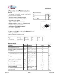
<strong>SiC</strong><br />
Silicon Carbide Diode<br />
5 th Generation thinQ! TM<br />
650V <strong>SiC</strong> Schottky Diode<br />
IDW 4 0 G 6 5 C 5<br />
<strong>Final</strong> <strong>Datasheet</strong><br />
Rev. 2.0 <br />
<strong>Power</strong> <strong>Management</strong> & <strong>Multimarket</strong>
5th Generation thinQ! <strong>SiC</strong> Schottky Diode<br />
IDW40G65C5<br />
1 Description<br />
Features<br />
Revolutionary semiconductor material - Silicon Carbide<br />
Benchmark switching behavior<br />
No reverse recovery/ No forward recovery<br />
Temperature independent switching behavior<br />
High surge current capability<br />
Pb-free lead plating; RoHS compliant<br />
Qualified according to JEDEC 1) for target applications<br />
Optimized for high temperature operation<br />
Benefits<br />
System efficiency improvement over Si diodes<br />
System cost / size savings due to reduced cooling requirements<br />
Enabling higher frequency / increased power density solutions<br />
Higher system reliability due to lower operating temperatures<br />
Reduced EMI<br />
Applications<br />
<br />
<br />
<br />
<br />
ThinQ! Generation 5 represents Infineon leading edge technology for<br />
the <strong>SiC</strong> Schottky Barrier diodes. Thanks to the more compact design and<br />
thin-wafer technology, the new family of products shows improved<br />
efficiency over all load conditions, resulting from both the improved<br />
thermal characteristics and a lower figure of merit (Qc x Vf).<br />
The new thinQ! Generation 5 has been designed to complement our<br />
650V CoolMOS families: this ensures meeting the most stringent<br />
application requirements in this voltage range.<br />
Switch mode power supply<br />
<strong>Power</strong> factor correction<br />
Solar inverter<br />
Uninterruptible power supply<br />
1 2<br />
1<br />
2<br />
3<br />
3<br />
CASE<br />
Table 1 Key Performance Parameters<br />
Parameter Value Unit<br />
V DC 650 V<br />
Q C ; V R =400V 55 nC<br />
E C ; V R =400V 14 µJ<br />
I F @ T C < 110°C 40 A<br />
Table 2 Pin Definition<br />
Pin 1 Pin 2 Pin 3<br />
n.c. C A<br />
Type / ordering Code Package Marking Related links<br />
IDW40G65C5 PG-TO247-3 D4065C5 www.infineon.com/sic<br />
1) J-STD20 and JESD22<br />
<strong>Final</strong> Data Sheet 2 Rev. 2.0, 2012-06-28
5th Generation thinQ! TM <strong>SiC</strong> Schottky Diode<br />
IDW40G65C5<br />
Table of contents<br />
Table of Contents<br />
1 Description .......................................................................................................................................... 2<br />
2 Maximum ratings ................................................................................................................................ 4<br />
3 Thermal characteristics ..................................................................................................................... 4<br />
4 Electrical characteristics ................................................................................................................... 5<br />
5 Electrical characteristics diagrams .................................................................................................. 6<br />
6 Package outlines ................................................................................................................................ 9<br />
7 Revision History ............................................................................................................................... 10<br />
<strong>Final</strong> Data Sheet 3 Rev. 2.0, 2012-06-28
5th Generation thinQ! TM <strong>SiC</strong> Schottky Diode<br />
IDW40G65C5<br />
Maximum ratings<br />
2 Maximum ratings<br />
Table 3 Maximum ratings<br />
Parameter Symbol Values Unit Note/Test Condition<br />
Min. Typ. Max.<br />
Continuous forward current I F – – 40<br />
Surge non-repetitive forward current,<br />
sine halfwave<br />
I F,SM<br />
T C < 110°C, D=1<br />
– – 182 T C = 25°C, t p =10 ms<br />
A<br />
– – 153 T C = 150°C, t p =10 ms<br />
Non-repetitive peak forward current I F,max – – 1432 T C = 25°C, t p =10 µs<br />
i²t value ∫ i²dt – – 166 A²s T C = 25°C, t p =10 ms<br />
Repetitive peak reverse voltage V RRM – – 650 V<br />
– – 118 T C = 150°C, t p =10 ms<br />
Diode dv/dt ruggedness dv/dt – – 100 V/ns V R =0..480 V<br />
<strong>Power</strong> dissipation P tot – – 183 W T C = 25°C<br />
Operating and storage temperature T j ;T stg -55 – 175 °C<br />
Mounting torque – 50 70 Ncm M3 and M4 screws<br />
3 Thermal characteristics<br />
Table 4 Thermal characteristics TO-247-3<br />
Parameter Symbol Values Unit Note/Test Condition<br />
Min. Typ. Max.<br />
Thermal resistance, junction-case R thJC – 0.6 0.8<br />
Thermal resistance, junctionambient<br />
Soldering temperature,<br />
wavesoldering only allowed at leads<br />
R thJA<br />
T sold<br />
– – 62<br />
K/W<br />
– – 260 °C<br />
leaded<br />
1.6mm (0.063 in.) from<br />
case for 10 s<br />
<strong>Final</strong> Data Sheet 4 Rev. 2.0, 2012-06-28
5th Generation thinQ! TM <strong>SiC</strong> Schottky Diode<br />
IDW40G65C5<br />
Electrical characteristics<br />
4 Electrical characteristics<br />
Table 5 Static characteristics<br />
Parameter Symbol Values Unit Note/Test Condition<br />
Min. Typ. Max.<br />
DC blocking voltage V DC 650 – –<br />
I R = 7 mA, T j = 25°C<br />
Diode forward voltage V F – 1.5 1.8 V I F = 40 A, T j =25°C<br />
– 1.8 2.2 I F = 40 A, T j =150°C<br />
Reverse current I R – 2.2 7000 V R =650 V, T j =25°C<br />
– 0.5 1800 µA V R =600 V, T j =25°C<br />
– 8.2 26500 V R =650 V, T j =150°C<br />
Table 6 AC characteristics<br />
Parameter Symbol Values Unit Note/Test Condition<br />
Total capacitive charge<br />
Q c<br />
Min. Typ. Max.<br />
– 55 nC<br />
Total Capacitance C – 1210 –<br />
V R =400 V, di/dt=200A/µs,<br />
I F ≤I F,MAX , T j =150°C.<br />
V R =1 V, f=1 MHz<br />
– 156 – pF V R =300 V, f=1 MHz<br />
– 155 – V R =600 V, f=1 MHz<br />
<strong>Final</strong> Data Sheet 5 Rev. 2.0, 2012-06-28
I F [A]<br />
I F [A]<br />
P tot [W]<br />
I F [A]<br />
5th Generation thinQ! TM <strong>SiC</strong> Schottky Diode<br />
IDW40G65C5<br />
5 Electrical characteristics diagrams<br />
Table 7<br />
<strong>Power</strong> dissipation<br />
Diode forward current<br />
200<br />
180<br />
160<br />
140<br />
120<br />
250<br />
200<br />
150<br />
0.1<br />
0.3<br />
0.5<br />
0.7<br />
1<br />
100<br />
80<br />
100<br />
60<br />
40<br />
50<br />
20<br />
0<br />
25 50 75 100 125 150 175<br />
T C [°C]<br />
P tot =f(T C ); R thJC,max<br />
0<br />
25 50 75 100 125 150 175<br />
T C [°C]<br />
I F =f(T C ); T j ≤175°C; R thJC,max ; parameter D=duty cycle<br />
Table 8<br />
Typical forward characteristics<br />
80<br />
Typical forward characteristics in surge current<br />
400<br />
70<br />
-55°C<br />
350<br />
60<br />
25°C<br />
300<br />
50<br />
100°C<br />
250<br />
-55°C<br />
40<br />
200<br />
25°C<br />
30<br />
20<br />
150°C<br />
175°C<br />
150<br />
100<br />
100°C<br />
150°C<br />
10<br />
50<br />
175°C<br />
0<br />
0 1 2 3<br />
V F [V]<br />
0<br />
0 1 2 3 4 5 6<br />
V F [V]<br />
I F =f(V F ); t p =200 µs; parameter: T j<br />
I F =f(V F ); t p =200 µs; parameter: T j<br />
<strong>Final</strong> Data Sheet 6 Rev. 2.0, 2012-06-28
Z th,jc [K/W]<br />
C [pF]<br />
Q C [nC]<br />
I R [A]<br />
5th Generation thinQ! TM <strong>SiC</strong> Schottky Diode<br />
IDW40G65C5<br />
Table 9<br />
Typ. capacitance charge vs. current slope 1)<br />
60<br />
Typ. reverse current vs. reverse voltage<br />
1.E-4<br />
50<br />
1.E-5<br />
40<br />
1.E-6<br />
30<br />
175°C<br />
20<br />
1.E-7<br />
150°C<br />
10<br />
1.E-8<br />
100°C<br />
25°C<br />
-55°C<br />
0<br />
100 300 500 700 900<br />
dI F /dt [A/µs]<br />
1.E-9<br />
100 200 300 400 500 600<br />
V R [V]<br />
Q C =f(di F /dt); T j =150°C; V R =400 V; I F ≤I F,max<br />
1) Only capacitive charge, guaranteed by design.<br />
I R =f(V R ); parameter: T j<br />
Table 10<br />
Max. transient thermal impedance<br />
Typ. capacitance vs. reverse voltage<br />
1<br />
1400<br />
1200<br />
1000<br />
0.1<br />
0.5<br />
0.2<br />
0.1<br />
0.05<br />
0.02<br />
0.01<br />
single pulse<br />
800<br />
600<br />
400<br />
200<br />
0.01<br />
1.E-06 1.E-03 1.E+00<br />
t p [s]<br />
Z th,jc =f(t P ); parameter: D=t P /T<br />
0<br />
0.1 1 10 100 1000<br />
V R [V]<br />
C=f(V R ); T j =25°C; f=1 MHz<br />
<strong>Final</strong> Data Sheet 7 Rev. 2.0, 2012-06-28
E C [µJ]<br />
5th Generation thinQ! TM <strong>SiC</strong> Schottky Diode<br />
IDW40G65C5<br />
Table 11<br />
Typ. capacitance stored energy<br />
40<br />
35<br />
30<br />
25<br />
20<br />
15<br />
10<br />
5<br />
0<br />
0 200 400 600<br />
V R [V]<br />
E C =f(V R )<br />
<strong>Final</strong> Data Sheet 8 Rev. 2.0, 2012-06-28
5th Generation thinQ! TM <strong>SiC</strong> Schottky Diode<br />
IDW40G65C5<br />
6 Package outlines<br />
Figure 1<br />
Outlines TO-247, dimensions in mm/inches<br />
<strong>Final</strong> Data Sheet 9 Rev. 2.0, 2012-06-28
5th Generation thinQ! TM <strong>SiC</strong> Schottky Diode<br />
IDW40G65C5<br />
Revision History<br />
7 Revision History<br />
5 th . Generation thinQ! TM <strong>SiC</strong> Schottky Diode<br />
Revision History: 2012-06-28, Rev. 2.0<br />
Previous Revision:<br />
Revision Subjects (major changes since last version)<br />
We Listen to Your Comments<br />
Any information within this document that you feel is wrong, unclear or missing at all<br />
Your feedback will help us to continuously improve the quality of this document.<br />
Please send your proposal (including a reference to this document) to: erratum@infineon.com<br />
Edition 2012-06-28<br />
Published by<br />
Infineon Technologies AG<br />
81726 Munich, Germany<br />
© 2012 Infineon Technologies AG<br />
All Rights Reserved.<br />
Legal Disclaimer<br />
The information given in this document shall in no event be regarded as a guarantee of conditions or<br />
characteristics. With respect to any examples or hints given herein, any typical values stated herein and/or any<br />
information regarding the application of the device, Infineon Technologies hereby disclaims any and all<br />
warranties and liabilities of any kind, including without limitation, warranties of non-infringement of intellectual<br />
property rights of any third party.<br />
Information<br />
For further information on technology, delivery terms and conditions and prices, please contact the nearest<br />
Infineon Technologies Office (www.infineon.com).<br />
Warnings<br />
Due to technical requirements, components may contain dangerous substances. For information on the types in<br />
question, please contact the nearest Infineon Technologies Office.<br />
The Infineon Technologies component described in this Data Sheet may be used in life-support devices or<br />
systems and/or automotive, aviation and aerospace applications or systems only with the express written<br />
approval of Infineon Technologies, if a failure of such components can reasonably be expected to cause the<br />
failure of that life-support, automotive, aviation and aerospace device or system or to affect the safety or<br />
effectiveness of that device or system. Life support devices or systems are intended to be implanted in the<br />
human body or to support and/or maintain and sustain and/or protect human life. If they fail, it is reasonable to<br />
assume that the health of the user or other persons may be endangered.<br />
<strong>Final</strong> Data Sheet 10 Rev. 2.0, 2012-06-28
w w w . i n f i n e o n . c o m<br />
Published by Infineon Technologies AG