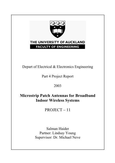
Microstrip Patch Antennas for Broadband Indoor Wireless Systems ...
Microstrip Patch Antennas for Broadband Indoor Wireless Systems ...
Microstrip Patch Antennas for Broadband Indoor Wireless Systems ...

You also want an ePaper? Increase the reach of your titles
YUMPU automatically turns print PDFs into web optimized ePapers that Google loves.
Depart of Electrical & Electronics Engineering<br />
Part 4 Project Report<br />
2003<br />
<strong>Microstrip</strong> <strong>Patch</strong> <strong>Antennas</strong> <strong>for</strong> <strong>Broadband</strong><br />
<strong>Indoor</strong> <strong>Wireless</strong> <strong>Systems</strong><br />
PROJECT – 11<br />
Salman Haider<br />
Partner: Lindsay Young<br />
Supervisor: Dr. Michael Neve
ABSTRACT<br />
The advantages of microstrip antennas have made them a perfect candidate <strong>for</strong> use in the<br />
wireless local area network (WLAN) applications. Though bound by certain<br />
disadvantages, microstrip patch antennas can be tailored so they can be used in the new<br />
high-speed broadband WLAN systems. This project concentrates on manufacture of<br />
broadband microstrip patch antennas <strong>for</strong> the 2.45 GHz ISM band and possible<br />
implementation using adhesive copper tape in research scenarios. In the course of the<br />
project, two broadband microstrip patch antennas were manufactured to adequately cover<br />
the 2.4- 2.5 GHz frequency band. A test procedure was also devised to compare the area<br />
coverage mappings, in term of path loss, of the in-house built antennas to the commercial<br />
broadband antennas. The testing show, the in-house antennas demonstrate larger<br />
bandwidth response compared to the commercial product but commercial product has a<br />
larger beamwidth and illustrate a better coverage.
ORIGINALITY DECLARATION<br />
This report is my own unaided work and was not copied from or written in collaboration<br />
with any other person.<br />
Signed: [ ]
ACKNOWLEDGEMENTS<br />
I would like to thank my project partner Lindsay Young <strong>for</strong> his contribution towards the<br />
project. I would also like to thank our Project Supervisor Dr. Michael Neve <strong>for</strong> all his<br />
support as well as all his help. It has been a privilege to work on the project under his<br />
supervision. I would also like to Nishant Khatri <strong>for</strong> providing us with additional<br />
in<strong>for</strong>mation and <strong>for</strong> sharing personal experience to aid our project.<br />
Finally I would like to acknowledge Mark Twiname <strong>for</strong> his technical assistance and <strong>for</strong><br />
sharing his expertise with the advanced radio equipment.
TABLE OF CONTENTS<br />
Page no<br />
1.0 Introduction 1<br />
2.0 <strong>Antennas</strong> <strong>for</strong> wireless LAN systems 2<br />
3.0 Foundations <strong>for</strong> <strong>Microstrip</strong> Design 3<br />
3.1 Polarization Types 3<br />
3.1.1 Linear Polarization 3<br />
3.1.2 Circular Polarization 4<br />
3.2 Bandwidth 4<br />
3.3 Feeding Techniques 5<br />
3.4 Substrate Permittivity 6<br />
4.0 Design Methodology 7<br />
5.0 Phase I 8<br />
5.1 Resonant Line Method 8<br />
5.2 Copper Tape 9<br />
5.3 Rectangular <strong>Patch</strong> 10<br />
5.3.1 Dimensions 10<br />
5.3.2 Length 10<br />
5.3.3 Width 11<br />
5.3.4 Co-axial probe feed 11<br />
5.3.5 Measurements 12<br />
6.0 Phase II 13<br />
6.1 <strong>Broadband</strong> Schemes 13<br />
6.2 Rectangular <strong>Broadband</strong> <strong>Patch</strong> using Parasitic Rings 14<br />
6.3 Rectangular <strong>Broadband</strong> Antenna 15<br />
6.4 Triangular <strong>Broadband</strong> Antenna 17<br />
7.0 Phase III 21<br />
7.1 Area Coverage Measurements 21<br />
8.0 Issues to consider <strong>for</strong> Future Research 23<br />
9.0 Future Recommendations 24<br />
9.1 Substrate 24<br />
9.2 Closer Input Impedance Match 24<br />
9.3 Reduction in Real-Estate Area 24<br />
9.4 Circularly Polarized <strong>Broadband</strong> <strong>Antennas</strong> 25<br />
9.5 Use of Other <strong>Broadband</strong> Schemes 25<br />
10.0 Conclusions 26<br />
11.0 Reference 27<br />
12.0 Appendices 28<br />
12.1 Appendix – A 28<br />
12.2 Appendix – B 29<br />
12.3 Appendix – C 30<br />
12.4 Appendix – D 32<br />
12.5 Appendix – E 33<br />
12.6 Appendix – F 35<br />
12.7 Appendix – G 36<br />
12.8 Appendix – H 37
TABLE OF FIGURES<br />
Page no<br />
1.0 Operations of <strong>Microstrip</strong> <strong>Patch</strong> 3<br />
2.0 Linear Polarization 4<br />
3.0 Circular Polarization 4<br />
4.0 Narrowband vs. <strong>Broadband</strong> 5<br />
5.0 Bandwidth Measurement 5<br />
6.0 Design methodology 7<br />
7.0 Implementation of resonant line method 8<br />
8.0 Conductivity of Copper tape 9<br />
9.0 Narrowband rectangular <strong>Patch</strong> Antenna 10<br />
10.0 VSWR response of Narrowband Rectangular <strong>Patch</strong> 12<br />
11.0 Effect of increasing the width of the <strong>Patch</strong> 12<br />
12.0 Rectangular <strong>Patch</strong> with the addition of Parasitic ring 14<br />
13.0 <strong>Broadband</strong> using Rectangular <strong>Patch</strong>es 15<br />
14.0 Effect of changing Feed location 16<br />
15.0 Effect of adding 1 Parasitic <strong>Patch</strong> 16<br />
16.0 VSWR response showing the effect of adding parasitic patches 17<br />
17.0 triangular Parasitic <strong>Patch</strong> Antenna 17<br />
18.0 VSWR response of a matched narrowband Triangular patch 18<br />
19.0 Smith chart plot showing the input impedance 19<br />
20.0 VSWR response showing the effect of addition of triangular parasitic patch 19<br />
21.0 VSWR response of in-house antennas against the commercial antenna 20<br />
22.0 Table of frequency used <strong>for</strong> each antenna 21<br />
23.0 Area Coverage shown in terms of path loss 22<br />
24.0 Insertion Loss of three substrates against frequency 23
1.0 INTRODUCTION<br />
Currently there is a boom in the development of personal communication service (PCS)<br />
devices as they are now deeply integrated into society. The PCS arena covers everything<br />
from cellular phones that incorporate digital cameras and web browsing to <strong>Wireless</strong><br />
Local Area Networks (WLAN). Since they can all be linked together, their applications<br />
are no longer limited. It is now both possible and af<strong>for</strong>dable to surf the web from your<br />
laptop without any wire connectivity, while enjoying the rugby match on your television.<br />
A WLAN is a flexible data communication network used as an extension to, or an<br />
alternative <strong>for</strong>, a wired LAN in a building. Primarily they are used in industrial sectors<br />
where employees are on the move, in temporary locations or where cabling may hinder<br />
the installation of wired LAN. Increasingly more and more wireless LANs are being<br />
setup in home and or home office situations as the technology is becoming more<br />
af<strong>for</strong>dable. Industry giants are already predicting that 90% of all notebooks will contain<br />
integrated WLAN by 2008. With progress and expansion comes the need <strong>for</strong> faster<br />
technology and higher transfer rates. The ongoing wireless LAN standardization and<br />
Research & Development activities worldwide, which target transfer rates higher than<br />
100 Mbps, justify the fact that WLAN technology will play a key role in wireless data<br />
transmission. Cellular network operators have recognized this fact, and strive to exploit<br />
WLAN technology and integrate this technology into their cellular data networks.<br />
The increasing popularity of indoor wireless LAN capable of high-speed transfer rate is<br />
prompting the development of efficient broadband antennas. Due to increased usage in<br />
residential and office areas, these systems are required to be low profile, aesthetically<br />
pleasing and low cost as well as highly effective and efficient. <strong>Microstrip</strong> patch antennas<br />
are well suited <strong>for</strong> wireless LAN application systems due to their versatility,<br />
con<strong>for</strong>mability, low cost and low sensitivity to manufacturing tolerances. Conventionally<br />
patch antennas have showed a narrowband response, implicating low bit rate transfer.<br />
Recently importance has been placed upon creating patch antennas that show broadband<br />
properties, capable of high-speed data transfer. The aim of this project is to design<br />
efficient and reliable broadband patch antennas showing signs of directivity leading to<br />
adequate area coverage and sufficient bandwidth usage.<br />
The following sections of the report will introduce the basic requirements of antennas <strong>for</strong><br />
wireless LAN systems (section 2). Foundations <strong>for</strong> microstrip design (section 3) will<br />
provide the basic ideas and background research in<strong>for</strong>mation. Design methodology<br />
(section 4) will offer a summary of the work that had been carried out in phase I, phase II<br />
and phase III (section 5, 6 and 7). The issues encountered throughout the project and<br />
future recommendations are explained in section 8 and 9. Finally project conclusions are<br />
presented in section 10.<br />
1
2.0 ANTENNAS FOR WIRELESS LAN SYSTEMS<br />
Currently the most commonly used WLAN system is the IEEE 802.11b system, with a<br />
maximum throughput of 11 Mbps using a narrowband system. Keeping on par with the<br />
growth of broadband connectivity in the landline sector, the new generation of WLAN<br />
systems are designed with a maximum throughput of at least 54 Mbps. <strong>Broadband</strong> refers<br />
to transmission of in<strong>for</strong>mation using a system that uses a comparatively larger frequency<br />
band, resulting in increases data transfer rate or throughput. If the broadband WLAN is to<br />
make an entry into the market and have an impact, it is important that the systems are<br />
versatile and per<strong>for</strong>ms extremely well. The broadband 802.11a system requires them to<br />
have a good coverage without failing signal strength. The range of coverage is dependent<br />
directly on the antenna per<strong>for</strong>mance hence the significance of the broadband antenna. A<br />
key requirement of a WLAN system is that it should be low profile, where it is almost<br />
invisible to the user. For this reason the microstrip patch antennas are the antennas of<br />
choice <strong>for</strong> WLAN use due to their small real estate area and the ability to be designed to<br />
blend into the surroundings.<br />
Many antenna designs are already present in the market that will successfully meet the<br />
broadband requirement. For example an omni-directional discone antenna is able to<br />
transmit in all direction and per<strong>for</strong>m extremely well over a very large bandwidth. These<br />
antennas are usually large metallic cumbersome objects and extremely indiscreet. Aside<br />
from the appearance, directivity and security are important features of WLAN systems.<br />
The system coverage often needs to be limited to designated areas, and since the 802.11x<br />
systems use the ISM bands, there are transmitted power limitations to reduce<br />
interference. It is important <strong>for</strong> the system to be highly directive in order to reduce<br />
coverage in unwanted areas. Primarily, it is due to possible LAN security breaches in<br />
case the LAN’s coverage extends outside the property and received by unwanted parties.<br />
The outside parties may then gain access to documents and other resources. Besides the<br />
security issue, there is also possible interference from neighbouring WLAN systems.<br />
There have been documented incidents in congested downtown business districts, where<br />
earlier WLAN systems per<strong>for</strong>m very poorly due to interference from neighbouring<br />
systems.<br />
As a result the demand has increased <strong>for</strong> broadband WLAN antennas that meet all the<br />
desired requirements. The <strong>Broadband</strong> antennas are required to be compact, low-profile,<br />
directive with high transmission efficiency and designed to be discreet. Due to these well<br />
met requirements coupled with the ease of manufacture and repeatability makes the<br />
<strong>Microstrip</strong> patch antennas very well suited <strong>for</strong> <strong>Broadband</strong> wireless applications.<br />
2
3.0 FOUNDATIONS FOR MICROSTRIP DESIGN<br />
A microstrip patch antenna is a radiating patch on one side of a dielectric substrate, which<br />
has a ground plane on the underside [1, pg-2]. The EM waves fringe off the top patch into<br />
the substrate, reflecting off the ground plane and radiates out into the air. Radiation<br />
occurs mostly due to the fringing field between the patch and ground.<br />
Ground<br />
plane<br />
<strong>Patch</strong><br />
Width<br />
Fig 1: Operations of a <strong>Microstrip</strong> <strong>Patch</strong><br />
Substrate<br />
The radiation efficiency of the patch antenna depends largely on the permittivity ( ε r ) of<br />
the dielectric. Ideally, a thick dielectric, low ε r and low insertion loss is preferred <strong>for</strong><br />
broadband purposes and increased efficiency. The advantages of microstrip antennas are<br />
that they are low-cost, con<strong>for</strong>mable, lightweight and low profile, while both linear and<br />
circular polarization is easily achieved. These attributes are desirable when considering<br />
antennas <strong>for</strong> WLAN systems. Some disadvantages include such as a narrow bandwidth as<br />
well as a low gain (~6 dB) and polarization purity is hard to achieve [2, pg-3].<br />
3.1 POLARIZATION TYPES<br />
This is the polarization of the wave radiated by the antenna in that particular<br />
direction. This is usually dependant on the feeding technique. When the direction is not<br />
specified, it is in the direction of maximum radiation [1]. Shown below are two most<br />
widely used polarization types.<br />
3.1.1 Linear Polarization<br />
A slot antenna is the counter part and the simplest <strong>for</strong>m of a linearly polarized<br />
antenna. On a slot antenna the E field is orientated perpendicular to its length dimension<br />
[3, pg-123]. The usual microstrip patches are just different variations of the slot antenna<br />
and all radiate due to linear polarization. Fig-2 illustrates the operations of a linearly<br />
polarized wave radiating perpendicular to the patch plane.<br />
3
Wave<br />
propagation<br />
E<br />
field<br />
3.1.2 Circular Polarization<br />
H<br />
field<br />
Fig 2: Linear Polarization<br />
Circular polarization (CP) is usually a result of orthogonally fed signal input.<br />
When two signals of equal amplitude but 90 o phase shifted the resulting wave is<br />
circularly polarized. Circular polarization can result in Left hand circularly polarized<br />
(LHCP) where the wave is rotating anticlockwise, or Right hand circularly polarized<br />
(RHCP) which denotes a clockwise rotation. The main advantage of using CP is that<br />
regardless of receiver orientation, it will always receive a component of the signal. This is<br />
due to the resulting wave having an angular variation.<br />
Wave<br />
Propagation<br />
(LHCP/ RHCP)<br />
3.2 BANDWIDTH<br />
Fee<br />
d<br />
Square<br />
<strong>Patch</strong><br />
Fig 3: Circular Polarization<br />
Orthogonal Input<br />
Couplar<br />
The bandwidth of the patch is defined as the frequency range over which it is<br />
matched with that of the feed line within specified limits [4, pg 11]. In other words, the<br />
frequency range over which the antenna will per<strong>for</strong>m satisfactorily. This means the<br />
channels have larger usable frequency range and thus results in increased transmission.<br />
The bandwidth of an antenna is usually defined by the acceptable standing wave ratio<br />
(SWR) value over the concerned frequency range. The fig 4 shows a typical broadband<br />
phenomenon in terms of frequency band usage.<br />
4
Fig 4: Narrowband vs. <strong>Broadband</strong><br />
Most commercial antennas use a 1.5:1 ratio, as shown in fig 5, suggesting that the<br />
range that is covered between the SWR of 1 up to 1.5 is the bandwidth. To ensure<br />
comparability with the commercial products, a decision was made to use a 1.5:1 ratio to<br />
calculate the bandwidth of antennas.<br />
Fig 5: Bandwidth Measurement<br />
5
3.3 FEEDING TECHNIQUES<br />
Feeding technique influences the input impedance and polarization characteristics<br />
of the antenna. There are three most common structures that are used to feed planar<br />
printed antennas. These are coaxial probe feeds, microstrip line feeds, and aperture<br />
coupled feeds. With coaxial probe feed the centre conductor of the coaxial connector is<br />
soldered to the patch. [4, pg 5] The coaxial fed structure is often used because of ease of<br />
matching the characteristic impedance to that of the antenna. Along with this, the<br />
parasitic radiation from the feed network tends to be insignificant. <strong>Microstrip</strong> line-fed<br />
structures are more suitable compared to probe feeds, due to ease of fabrication and lower<br />
costs. Serious drawbacks of this feed structure are the strong parasitic radiation and it<br />
requires a trans<strong>for</strong>mer, which restricts the broadband capability of the antenna [4]. The<br />
aperture-coupled structure has all of the advantages of the <strong>for</strong>mer two structures and<br />
isolates the radiation from the feed network thereby leaving the main antenna radiation<br />
uncontaminated.<br />
Initially the plan was to use microstrip feedline but after considering all the<br />
possibilities it was decided to use coaxial probe feed technique. This decision was made<br />
due to incapability of microstrip line-fed structure to per<strong>for</strong>m under broadband<br />
conditions, due to its inability provide a good match over a large band of frequency.<br />
3.4 SUBSTRATE PERMITTIVITY<br />
The dielectric constant plays a major role in the overall per<strong>for</strong>mance of the<br />
antenna. It affects both the width, in turn the characteristic impedance and the length<br />
resulting in an altered resonant frequency and reduced transmission efficiency. Initially<br />
we are using the G10 fiberglass substrate (also known as FR4) but the permittivity ( ε r )<br />
of the substrates alters from batch to batch, sometimes even between different sheets of<br />
the substrate. Three different methods were investigated to determine theε r .<br />
- The Napoli-Hughes opened edged cavity method [5]: this method uses a dielectric<br />
with copper on both sides of the substrate. When tested the results would show<br />
sharp spikes at resonant frequencies. This can be used to determine theε eff .<br />
However, this method is often deemed inaccurate.<br />
- The closed cavity method [5]: The setup is somewhat similar to the previous<br />
method, except the edges of the copper are short-circuited. As a result only the<br />
Non-TEM waves propagate. However, this method is very complicated to<br />
implement.<br />
For the purpose of this project, the third method known as the resonant line<br />
method was implemented due to its ease of fabrication and its ability to generate good<br />
approximations [1], [2]. The resonant line method is explained in detail in section 5.<br />
6
4.0 DESIGN METHODOLOGY<br />
In order to reach the primary goal of manufacturing broadband patch antennas the project<br />
was split into subtasks, which allowed <strong>for</strong> achievable short-term goals. After the initial<br />
research regarding microstrip antennas specific work needed to be done. The flow chart<br />
(fig 6) explains the process.<br />
Research<br />
Determining substrate<br />
permittivity<br />
Design feed impedance<br />
matched narrowband patch<br />
Investigate possible broad<br />
band techniques<br />
Design two broadband<br />
patches<br />
Benchmark against<br />
commercial broadband<br />
product<br />
Fig 6: Design Methodology<br />
During phase 1 of the project, we used the resonant line method to calculate the<br />
permittivity of the G10 fiberglass substrate. This process had to be carried several times<br />
to reach accuracy, as each new batch of substrates has slightly different permittivity.<br />
Using accurate permittivity values and the equations given in the book “<strong>Microstrip</strong> <strong>Patch</strong><br />
Antenna” [1], the narrowband rectangular patch was designed. Phase one also oversaw<br />
the introduction of copper tapes to manufacture patches. Phase two involved in-depth<br />
technical research regarding possible broadband techniques. The best scheme was chosen<br />
based on manufacturing simplicity without compromising per<strong>for</strong>mance over the<br />
frequency band concerned. Two broadband patches were produced during this phase;<br />
both the patches were thoroughly tested <strong>for</strong> bandwidth (BW) and tuned to best match the<br />
input impedance. Phase 3 observed the field per<strong>for</strong>mance and area coverage<br />
measurements. Path loss was measured <strong>for</strong> both antennas and compared to the<br />
commercial broadband antenna.<br />
7
5.0 PHASE I<br />
5.1 RESONANT LINE METHOD:<br />
Accurately determining the dielectric constant ε r is critical to the antenna design<br />
process when designing broadband antennas. The Resonant Line method was chosen due<br />
to its ease of implementation and the return of accurate approximations. This method uses<br />
two microstrip transmission line structures as shown below:<br />
1mm 1mm<br />
l<br />
1<br />
30mm 100mm<br />
30mm<br />
1mm<br />
l2<br />
1mm<br />
30mm 200mm<br />
30mm<br />
Fig 7: Implementation of resonant line method<br />
One point to note is that, though in the illustration the lines are shown on one<br />
board, they need to be on separate boards or else coupling will occur resulting in highly<br />
inaccurate results. When a signal is fed into the input port, the gaps act as open circuits<br />
and in turn set up zero current at these points. When the signal frequency has a<br />
wavelength that is a factor (e.g. λ / 2 , λ etc) of the length of the centre section, the<br />
received signal at the output port will peak. The output will peak every time the signal<br />
wavelength matches the integral number of λ / 2 of the centre section. The wavelength<br />
( λ ) is known and frequency of the signal can be observed using the network analyzer.<br />
The length l2 is twice the size of length l1 to compensate <strong>for</strong> the fringing effect at the ends<br />
of the patch. The equations (1) and (2) can be used to workout the dielectric constants,<br />
ε eff andε r :<br />
ε<br />
eff<br />
⎡c<br />
=<br />
⎣<br />
( ) 2<br />
n f − n f ⎤<br />
1 2 2 1<br />
ε eff ⎢<br />
⎥<br />
(1)<br />
2 f1<br />
f 2 ( l2<br />
− l1)<br />
ε r + 1 ε r −1<br />
⎛ h<br />
= + ⎜1+ 12<br />
2 2 ⎝ W<br />
Please refer to Appendix B <strong>for</strong> a step-by-step method <strong>for</strong> ε eff andε r calculations.<br />
The results suggested an average value of 4.4 <strong>for</strong> the ε r [Refer to Appendix B]. This ε r<br />
value is lower then the G10 substrate permittivity calculated in the previous years [6]. A<br />
possible reason <strong>for</strong> this could be the use of the new milling machine. When stripping the<br />
⎦<br />
⎞<br />
⎟<br />
⎠<br />
−1/<br />
2<br />
8<br />
(2)
extra copper from the substrate, the machine removed a significant amount of substrate<br />
resulting in reduced height and ripples along the substrate plane. Due to this effect, our<br />
measurements reflected incorrect results. It was found theε r of 4.43 (2.4 GHz) using the<br />
adhesive copper tape, to be adequate where projects from previous results show an<br />
average ε r value of 4.5.<br />
5.2 COPPER TAPE<br />
It was decided to investigate the use of adhesive copper tape to manufacture<br />
patches autonomously after a suggestion from Dr. Michael Neve; this meant the project<br />
was no longer bound by the manufacturing turn around delay period. A 3M product that<br />
fit project requirements was found and ef<strong>for</strong>ts were made to acquire a roll of adhesive<br />
copper tapes. Reputedly the copper tapes have been used to manufacture antennas that<br />
resonate up to 5GHz. The patches made from the copper tape, can be placed on single<br />
copper sided sheets of substrate and allow the user to create their own microstrip patch<br />
antennas without the use of any industrial machines or etching process. As a result the<br />
manufacture time can be reduced down to a few, which meant manufacture of boards was<br />
no longer PCB milling machine reliant. The copper tape allowed us to cut the copper tape<br />
to fit calculated dimensions and create desired microstrip patches. One side of the tape<br />
was adhesive; so it was possible to fix them on the substrates and in some cases overlap<br />
them. But some concerns were raised about the conductivity of the glue. An experiment<br />
was devised, to measure the transmission loss <strong>for</strong> a thin unbroken strip of copper tape.<br />
The test was repeated <strong>for</strong> a copper tape strip of identical dimensions with a missing<br />
section that was being covered by an overlapped copper tape joining the ends. The tests<br />
show (fig 8) the difference between copper strip and overlapped copper tape is minimal<br />
and can be ignored.<br />
Fig 8: Conductivity of copper tape<br />
9
5.3 RECTANGULAR PATCH<br />
The purpose of manufacturing a rectangular narrowband patch was to gain some<br />
of the insights to the patch design process. Based on the measurements acquired from the<br />
narrowband rectangular antenna, the broadband antennas were designed. Especially to<br />
calculate the probe feed coordinates and the iterative process involved. The linearly<br />
polarized narrowband antenna was designed to operate at 2.45 GHz with input impedance<br />
of 50 ohms, using G10 fiberglass substrate.<br />
5.3.1 Dimensions<br />
dL<br />
5.3.2 Length<br />
Length<br />
Feed Location<br />
Width<br />
Fig 9: Narrowband Rectangular <strong>Patch</strong> Antenna<br />
dL<br />
Fringing<br />
Field<br />
The length of the patch determines the resonant frequency thus it is a critical<br />
factor because it is a narrowband patch. The equation shown below was used to calculate<br />
the length of the patch. Since the fringing field cannot be accounted <strong>for</strong> accurately none<br />
of the results are definite.<br />
C<br />
L = − 2×<br />
dL<br />
(3)<br />
2 f ε<br />
r<br />
eff<br />
For Frequencies below 2 GHz, the variation in L with h is almost negligible [1,<br />
Pg-57]. This is a good approximation, as long as resonant frequency (fr) is less than<br />
2GHz. The dL is the length extension due to the fringing field and can be calculated<br />
using the equation 4.<br />
( ε + 0.<br />
3)(<br />
W / h + 0.<br />
264)<br />
dL = 0.<br />
412h<br />
( ε<br />
eff<br />
eff<br />
− 0.<br />
258)(<br />
W / h +<br />
0.<br />
8)<br />
There are other equations, which can be used to approximate dL, but the Eq-4 has been<br />
shown to give better results [1, Pg-46]. Incorporating both Eq 4 and Eq 5, a theoretical<br />
10<br />
(4)
<strong>Patch</strong> length of 29.66 mm was determined using EXCEL spreadsheets [Refer to<br />
Appendix-B].<br />
5.3.3 Width<br />
The width is critical in terms of power efficiency, antenna impedance and<br />
bandwidth. It is largely dependent on the operating frequency and the substrate dielectric<br />
constant. The equation below was used to workout the width of the patch. Other widths<br />
could have been used but if it is too small then radiator efficiency will suffer and if it is<br />
too large higher order modes will be excited, resulting in field distortions [1, pg-57].<br />
C ⎛ ε r + 1⎞<br />
W = ⎜ ⎟<br />
(5)<br />
2 fr<br />
⎝ 2 ⎠<br />
The theoretical width was calculated to be 37.86 mm. Refer to Appendix-B <strong>for</strong><br />
the spreadsheet implementing Eq-5.<br />
5.3.4 Co-axial Probe Feed<br />
An advantage of this technique is that it can be placed at any location, and the<br />
impedance match will depend on its location on the patch. Using the equation provided in<br />
Bahl/Bhartia [1] we can approximate the feed coordinate, which would match the input<br />
impedance to a 50-Ohm feeder. An improved impedance match will ideally increase the<br />
bandwidth, the return loss and improve per<strong>for</strong>mance by reducing the excitation of<br />
unwanted modes of radiation. The feed co-ordinates were calculated using the following<br />
equation:<br />
Xf (along the length) =<br />
L<br />
2 ξ ( l)<br />
re<br />
The calculated feed coordinates <strong>for</strong> the given rectangular patch operating at 2.45<br />
GHz are Yf = 7.52 mm and Xf = 18.79 mm. But this equation is an approximation and<br />
will only provide the starting point. It is very much an iterative process, to workout the<br />
exact co-ordinates that will match the impedance of the feedline to the antenna. Using the<br />
Network analyzer, the following coordinates returned the best impedance match. AT Yf =<br />
7.00 mm and Xf = 20 mm, at an input impedance of 49.84–0.012j ohms. However it was<br />
found as the feed point was moved downwards from the calculated coordinates, the<br />
impedance match improved. But there was a threshold point beyond which, the match<br />
started to deteriorate.<br />
−1/<br />
2<br />
W<br />
Yf (along the width) =<br />
2<br />
ε<br />
r + 1 ε r −1<br />
⎛ h ⎞<br />
where ξ re (l)<br />
= + ⎜1+ 12 ⎟<br />
2 2 ⎝ L ⎠<br />
−1/<br />
2<br />
11<br />
(6)<br />
(7)
5.3.5 Measurements:<br />
The graphs below show (Fig 10) the SWR response of the rectangular input<br />
impedance matched antenna, using the HP8510 network analyzer. The plots of return loss<br />
and the smith charts are also provided in Appendix-D.<br />
VSWR<br />
5<br />
4.5<br />
4<br />
3.5<br />
3<br />
2.5<br />
2<br />
1.5<br />
1<br />
2.1 2.2 2.3 2.4 2.5 2.6 2.7<br />
Frequency (GHz)<br />
Fig 10: VSWR response Narrowband Rectangular <strong>Patch</strong> antenna<br />
The Book written by Girish Kumar and K.P Ray, recommends widening the width of the<br />
patch to increase bandwidth [REFERNCE]. In order to test the suggestion, the width was<br />
increased to 60 mm, which increased the bandwidth to 112 MHz at VSWR 2:1. But fig<br />
11 fails to illustrate clearly the resonant frequency shift and the instability suffered by the<br />
input impedance match due to excitation of higher order resonance modes [4].<br />
VSWR<br />
5<br />
4.5<br />
4<br />
3.5<br />
3<br />
2.5<br />
2<br />
1.5<br />
1<br />
2.1 2.2 2.3 2.4 2.5 2.6 2.7<br />
Frequency (GHz)<br />
40mm<br />
60mm<br />
Fig 11: Effect of increasing the Width of the <strong>Patch</strong><br />
12
6.0 PHASE II<br />
6.1 BROADBANDING SCHEMES<br />
Considerable amount of research time was invested in finding a technique that<br />
was easy to implement using adhesive copper tapes as well as projecting a low<br />
manufacturing period and cost. In order to increase bandwidth using thicker substrates<br />
with low ε r [3, Pg-37] was considered. However practical limitation prevents increasing<br />
the height of the substrate since h ≥ 0. 1λ0<br />
, antenna per<strong>for</strong>mance degrades due to<br />
unwanted surface-wave propagations. Stacked Multi-resonators which are<br />
electromagnetically coupled microstrip antennas can also widen BW. The use of ferrite<br />
substrate and the use of log-periodic configurations were also considered. Explained<br />
below are some of the broadband schemes under serious consideration.<br />
- Planar Multi-resonators: the patches are etched close to each other and the gap in<br />
between should not exceed 2h. A single resonator is directly excited while the<br />
others are either parasitically coupled or connected through shorting strips [4,Pg-<br />
89].<br />
- Stacked Electromagnetically coupled patches: similar to the last method but<br />
instead the patches are stacked on top of each other [4, Pg-171]. The patches are<br />
placed on different layers of the dielectric substrates so the total area stays the<br />
same. Different patches are either coupled electromagnetically or aperture<br />
coupled.<br />
- Compact broadband <strong>Microstrip</strong> antennas: since this project aims to develop<br />
antennas <strong>for</strong> the broadband WLAN this model is very important, as ultimately the<br />
antenna real estate needs to be minimized. Increasing the dielectric constant,<br />
which reduces the area but results in reduced BW and gain, does this. Using this<br />
technique the regular shaped patches (rectangle, circle etc) are modified by<br />
inserting posts that act as short circuits [4, Pg-205], thus increasing the BW.<br />
After considerable amount of research and considering the above schemes, the<br />
decision was made to use the parasitically coupled broadband technique. Due to ease of<br />
manufacture using copper tapes, which meant greatly reduced manufacturing time and<br />
flexibility to make alterations quickly to adequately match the input impedance over the<br />
frequency range. The research shows, even though other methods may return higher<br />
bandwidth, the achievable BW using parasitic patches is sufficient to cover the 2.4 - 2.5<br />
GHz frequency band [3, 4].<br />
13
6.2 RECTANGULAR BROADBAND PATCH USING PARASITIC RINGS<br />
L<br />
W<br />
Feed Location<br />
W<br />
(parasitic)<br />
L<br />
(parasitic)<br />
Fig 12: Rectangular <strong>Patch</strong> with the addition of parasitic ring<br />
Initially, the ideas of using parasitic rings to increase the bandwidth seem<br />
appealing. The scheme indicated reduced real estate without sacrificing bandwidth [4].<br />
Following the general design shown in fig 12, ‘t’ is the thickness of the parasitic ring and<br />
‘d’ is the gape between the parasitic ring and the base resonator. A number of patches<br />
were designed, all of varying ‘t’ and ‘d’, so the changes could be observed. Un<strong>for</strong>tunately<br />
none of the patches showed any broadband activities.<br />
Further research suggested, the length of the parasitic ring cannot be larger then<br />
the base resonator which controlled the base resonant frequency. This would suggest, the<br />
result of having a ring larger than the base patch would cause the ring to resonate at a<br />
frequency outside the 2.4 - 2.5 GHz range. It was also noted that, reducing the gap<br />
between the base patch and the ring would increase coupling and increase radiation and<br />
possibly increase bandwidth. Due to time restriction, this design scheme was not pursued<br />
further. However a method was discovered further into the project that would allow this<br />
scheme to be implemented effectively. This method will be described in detail later in<br />
section 9.3.<br />
14
6.3 RECTANGULAR BROADBAND ANTENNA<br />
L4<br />
W4<br />
W1<br />
W<br />
Feed Location<br />
W2<br />
L<br />
L1<br />
L2<br />
Fig 13: <strong>Broadband</strong> using Rectangular <strong>Patch</strong>es<br />
The parasitic patch method was chosen because its mechanism of operations is<br />
fashioned similar to the parasitic ring but without the restrictions suffered by the previous<br />
method. In this method, instead of using parasitic rings, parasitic patches of similar<br />
dimensions are placed around the base fed-patch. Operation of the parasitic are same as<br />
the base patch as in the length of the parasitic patch determines the resonant frequency<br />
and the width sets the bandwidth. The fig-13 shown above is a typical topographical<br />
layout of a four parasitic element patch antenna. It is important to note that the parasitic<br />
element dimensions are not identical to each other. By changing individual dimensions it<br />
is possible to tune the antenna to achieve the best possible broadband solution. It is<br />
important to keep in mind that, it is hard to notice the difference caused by altering the<br />
dimensions of one parasitic element. But rather, all four elements need to be altered<br />
together in a logical manner in order to achieve the overall broadband solution.<br />
Initially when designing the antenna, all four parasitic elements had identical<br />
dimension as the base patch. Subsequently the lengths of the parasitic elements were<br />
altered until the required resonant frequencies were achieved. It soon became apparent<br />
due to the addition of parasitic elements, the feed location needed to be changed in order<br />
to provide the optimum input impedance match. Further research suggested this issue<br />
could be resolved by shifting the feed location towards the bottom edge of the antenna [4,<br />
pg 109]. The effect of shifting the feed location 3mm closer can be seen in fig 13. The<br />
appropriate smith chart of the above occurrence can be found in Appendix-E.<br />
W2<br />
L3<br />
15
VSWR<br />
3<br />
2.8<br />
2.6<br />
2.4<br />
2.2<br />
2<br />
1.8<br />
1.6<br />
1.4<br />
1.2<br />
1<br />
2.1 2.2 2.3 2.4 2.5 2.6 2.7<br />
Frequency (GHz)<br />
Fig 14: Effect of changing Feed location<br />
Original feed<br />
Revised feed<br />
Even though at first the SWR reflected a poor impedance match, as shown in fig 14, the<br />
positive effects of shift became apparent after adding the first parasitic element.<br />
VSWR<br />
3<br />
2.8<br />
2.6<br />
2.4<br />
2.2<br />
2<br />
1.8<br />
1.6<br />
1.4<br />
1.2<br />
1<br />
2.1 2.2 2.3 2.4 2.5 2.6 2.7<br />
Frequency (GHz)<br />
Fig 15 Effect of adding 1 parasitic patch<br />
No parasitic elements<br />
One Parasitic Element<br />
The resulting broadband behaviour is obvious from the fig 15 above but the resulting<br />
bandwidth was not acceptable. It returned a bandwidth of only 31 MHz (VSWR 1.5:1)<br />
covering the 2.501 GHz to 2.532 GHz frequency range.<br />
16
VSWR<br />
3<br />
2.8<br />
2.6<br />
2.4<br />
2.2<br />
2<br />
1.8<br />
1.6<br />
1.4<br />
1.2<br />
1<br />
2.1 2.2 2.3 2.4 2.5 2.6 2.7<br />
Frequency (GHz)<br />
Narrow Band<br />
One Element<br />
Two Elements<br />
Four Elements<br />
Fig 16: VSWR response showing the effect of adding parasitic patches<br />
The eventual emergence of the rectangular parasitic patch antenna (fig 16) produced a<br />
bandwidth of 185.5 MHz amid VSWR of 2:1 over the frequency range of 2.3695MHz to<br />
2.555MHz. The only noticeable flaw was at frequency 2.47 GHz the VSWR fell outside<br />
the 1.5:1 range, resulting in failure to meet stringent commercial specifications. For the<br />
smith chart plot illustrating the input impedance of the antenna please refer to Appendix-<br />
E.<br />
6.4 TRIANGULAR BROADBAND ANTENNA<br />
After successfully commissioning the rectangular parasitic patch antenna, the<br />
attention turned towards reducing the real estate area while maintaining the per<strong>for</strong>mance<br />
previously achieved. Triangular patches hold similar attributes as rectangular patches<br />
while covering using a smaller area. The triangular patches also have wide half-power<br />
beam widths in both planes. There<strong>for</strong>e it is suitable <strong>for</strong> hemispherical application [1,<br />
pg151]. In this case, an Equilateral Triangular microstrip antenna (ETMSA) is used since<br />
they have been known to return a larger bandwidth [4, Pg-126] compared to other<br />
triangular antenna.<br />
S1<br />
Fig 17: Triangular Parasitic <strong>Patch</strong><br />
y<br />
S2<br />
h<br />
17
Eq 8 will return the dimensions of a triangular patch where f is the lowest order<br />
resonant frequency; S is the length of the side arm and ε r is the substrate permittivity.<br />
2C<br />
f = (8)<br />
3S<br />
ε<br />
The design method that proved very effective while producing the previous<br />
broadband antenna, also proved useful when producing the triangular broadband antenna.<br />
Initially the narrowband triangular patch was made using the copper tape and tuned to<br />
match the input impedance. The initial construction led to the patch resonating at a<br />
frequency higher then 2.45 GHz. Numerous attempts were required be<strong>for</strong>e the correct<br />
dimensions were achieved which allowed the patch to resonate at 2.43 GHz. It was<br />
deliberately tuned <strong>for</strong> 2.43 GHz keeping in mind the frequency shift that will occur from<br />
adding parasitic elements. Input impedance was found to be very large at the vertex along<br />
the feed axis. The 50-ohm impedance matching can be obtained by feeding the antenna at<br />
either above or below the null position at the centre of the patch [4, pg 81]. The optimum<br />
feed coordinates were found to be Yf = 19 mm, Xf = 19 mm, where the narrow band<br />
antenna returned an input impedance of 47.66+0.76j ohms. Fig 17 shows the per<strong>for</strong>mance<br />
of a matched narrowband triangular patch. The narrowband antenna had a bandwidth of<br />
91 MHz using 2:1 VSWR and 53 MHz using 1.5:1 VSWR. Please refer to Appendix-F<br />
<strong>for</strong> return loss plots and input impedance charts of the narrowband triangular antenna.<br />
Fig 18: VSWR response of a matched Narrowband Triangular <strong>Patch</strong><br />
Using the proven narrowband patch as the base resonator, the parasitic patches<br />
were added to extend its bandwidth. The next step was to add a parasitic element<br />
designed to resonate at 2.48 GHz, resulting in a BW spread in the 2.5 GHz direction. The<br />
fig 20 shows the effect of adding one extra parasitic ring. Even though the per<strong>for</strong>mance<br />
was promising, the return loss showed the power outage was lacking. It was found that<br />
the best way to tune these antennas is to follow the changes in smith chart. Looking at fig<br />
19 we can see the narrowband has no loop in its smith chart. The aim is to create the<br />
loops by adding parasitic elements but also tune the antenna so the loops are situated<br />
around the centre of the smith chart. This will ensure a good input impedance match over<br />
a larger range of frequencies. Larger loops provide greater BW extension, and this is<br />
r<br />
18
evident from the BLACK plot in the smith chart which is the final antenna and it has the<br />
largest loops and all centred on the midpoint in the smith chart.<br />
Fig 19Smith chart showing the input impedance of all triangular broadband patch over 2.1 - 2.8 GHz<br />
With the addition of the second parasitic element, resonating at a slightly lower<br />
frequency, the extra dip in the SWR plot was added. This extended the coverage in the<br />
2.4 GHz end of the frequency band. It was also found that overall resonance range could<br />
be shifted not only by the dimensions alone but also the gap between the parasitic and<br />
base element. By utilizing this feature, it is possible to keep one end of the resonant band<br />
stable while extending the other end of the frequency band. As a result the parasitic<br />
elements of the ETMSA are not symmetrically distanced from the base resonator.<br />
Fig 20: VSWR response showing the effect of addition of triangular parasitic patch<br />
19
A key issue that surfaced during the implementation of the antenna was the<br />
impedance matching process. The matching process is somewhat different <strong>for</strong> the gap<br />
coupled parasitic resonators. The input impedance of the base resonator needs to be<br />
greater then 50 ohms since the addition of the parasitic elements will create the loops that<br />
pull down the overall impedance resulting in a closer match at the desired frequencies.<br />
Using the HP8510 network analyser, it is possible to show (fig 20) that the triangular<br />
ETMSA produced a 259 MHz bandwidth using VSWR 2:1 and 198 MHz using VSWR<br />
1.5:1. Using VSWR 2:1, the bandwidth of the triangular antenna is 2.85 times greater<br />
than the narrowband antenna and 1.4 times greater then the rectangular broadband<br />
antenna. Please refer to Appendix-G <strong>for</strong> return loss plots of the broadband Triangular<br />
patch antenna.<br />
The triangular broadband also produced a maximum of 42.535 dB return loss at<br />
2.4325 GHz. Please refer to Appendix-G <strong>for</strong> return loss response of the antennas. Also<br />
The <strong>Patch</strong> real estate required <strong>for</strong> the triangular is 90 cm 2 compared to the 210.6 cm 2 <strong>for</strong><br />
the rectangular patch. As the fig 21 illustrates, the triangular has a larger bandwidth and<br />
produces a greater maximum return loss. But at a higher frequency, the parasitic element<br />
is resonant, and there<strong>for</strong>e experiences a large phase delay with respect to the base<br />
resonator; hence the beam maximum shifts away from the broadside [4, pg 125]. Please<br />
refer to Appendix-H <strong>for</strong> a comparison in terms of return loss and input impedance.<br />
Fig 21: VSWR response of two in-house broadband antennas against the commercial broadband<br />
antenna<br />
20
7.0 PHASE III<br />
7.1 AREA COVERAGE MEASUREMENTS<br />
Instead of using an anechoic chamber to estimate the radiation pattern using the<br />
electric and magnetic field, the decision was made to use Alex Wong’s testing apparatus.<br />
The testing equipment calculates the path of loss of each of the antennas at different spots<br />
of a room. High frequency signal generators were used to feed the antennas. And using<br />
radio receiver and a balun based stepper motor driven antenna, 360 samples of path loss<br />
are taken <strong>for</strong> the three resonating antennas. The average path loss of the 360 samples is<br />
taken to be the path loss of the antenna at a given spot in the room. The two broadband<br />
antennas were tested along with the commercial antenna, and the results were compared<br />
to benchmark the in-house antennas.<br />
Three resonating frequencies were chosen, 100 KHz apart, <strong>for</strong> the three antennas.<br />
However the return losses of the antennas are not constant and they are very dissimilar.<br />
We had to be careful not to pick a frequency that returned a very high return loss <strong>for</strong> one<br />
antenna but comparatively poor return loss <strong>for</strong> the other two. As a result, to reduce bias,<br />
three frequencies were chosen that provided almost identical return losses <strong>for</strong> all three<br />
antennas, as shown in fig 22.<br />
Triangular Rectangular Commercial<br />
Frequency<br />
(MHz)<br />
Return<br />
2458 2459 2460<br />
Loss (dB) -13 -13.5 -14<br />
Fig 22 Table of frequency used <strong>for</strong> each antenna<br />
For the measurements to be correct, all the losses needed to be accounted <strong>for</strong> and<br />
entered in the software <strong>for</strong> reliable results. The individual feeder losses were calculated,<br />
and also the actual power at the antenna end from the signal generators. They were both<br />
calculated using the test receiver and a step attenuator. In order to per<strong>for</strong>m tests that were<br />
truly representative and emulate a typical office situation, the radio lab (R4) was chosen.<br />
11 spots were chosen, that approximately covered the perimeter of the room. Obviously<br />
further testing is required but due to time constriction, the decision was made to restrict<br />
testing to one room only.<br />
As shown in fig 23, in terms field per<strong>for</strong>mance the commercial antenna outper<strong>for</strong>ms<br />
the in-house antennas. It is also evident that, in most cases the rectangular<br />
antenna per<strong>for</strong>ms better than the triangular antenna. The overall maximum difference<br />
between the commercial and the in-house antennas is approximately 10 dB.<br />
Further schematics of the room and exact testing spots and path loss results are provided<br />
in the Appendix-C.<br />
Possible causes <strong>for</strong> the in-house antennas <strong>for</strong> under-per<strong>for</strong>ming can be put down to the<br />
substrate anomalies at high frequency and a comparatively poor input impedance match.<br />
21
100<br />
80<br />
60<br />
40<br />
20<br />
0<br />
100<br />
80<br />
60<br />
40<br />
20<br />
0<br />
100<br />
80<br />
60<br />
40<br />
20<br />
0<br />
11<br />
Mark Twiname’s Office<br />
10<br />
9<br />
100<br />
80<br />
60<br />
40<br />
20<br />
0<br />
100<br />
80<br />
60<br />
40<br />
20<br />
0<br />
8<br />
100<br />
80<br />
60<br />
40<br />
20<br />
Legend<br />
4<br />
5<br />
0<br />
100<br />
80<br />
60<br />
40<br />
20<br />
0<br />
7<br />
Door<br />
100<br />
80<br />
60<br />
40<br />
20<br />
6<br />
Triangular Antenna<br />
Rectangular Antenna<br />
Commercial Antenna<br />
All measurements are Path Loss in dB.<br />
Smaller bars are better.<br />
0<br />
<strong>Antennas</strong><br />
placed<br />
here<br />
Network<br />
Analyser<br />
Fig 23: Area Coverage shown in terms of path loss (dB)<br />
100<br />
80<br />
60<br />
40<br />
20<br />
0<br />
100<br />
80<br />
60<br />
40<br />
20<br />
Network Analyser Room<br />
0<br />
1<br />
100<br />
80<br />
60<br />
40<br />
20<br />
0<br />
2<br />
Entrance<br />
3<br />
Screened Room<br />
22
8.0 ISSUES TO CONSIDER FOR FUTURE RESEARCH<br />
A major hurdle the project suffered from was the inability of the new PCB milling<br />
machine to produce high frequency PCB boards. When removing the extra copper from<br />
the substrate, the machine removed significant amount of substrate, resulting in reduced<br />
height and also creating ripples along the substrate plane. As a result the calculated ε r<br />
was incorrect, ensuing incorrect antenna dimensions and changing antenna behavior. The<br />
milling machine also had a turn around period of a few weeks. Due to these facts, we<br />
were <strong>for</strong>ced to investigate other viable options and ultimately the use of adhesive copper<br />
tapes. The use of copper tapes meant there was no turn around period and allowed us to<br />
resize the dimensions quickly and test the difference. This led to quick impedance<br />
matching within a small period of time. Consequently broadband antennas require a good<br />
impedance match to per<strong>for</strong>m and require a process where each result builds upon the last<br />
in order to achieve an adequate match.<br />
In deciding to use the copper tape, the active decision was made to trade off<br />
accuracy <strong>for</strong> time. It is imperative to be extremely accurate when incising the dimensions<br />
from the copper tape, because a difference of 0.5mm can shift the resonating frequency of<br />
the patch. A decision was made early on, to produce two boards <strong>for</strong> each design, to make<br />
sure that the results can be repeatable. It is important to account <strong>for</strong> all the feeder losses<br />
in order to obtain truly representative results. Individual feeder looses were measured<br />
using the test receiver and a step attenuator. Where a known attenuation is placed in<br />
series with the signal generator and connected to the test receiver. Since the generator<br />
output is known along with the attenuation, it is possible to account <strong>for</strong> the extra losses<br />
due to the feeder and the insertion loss introduced by the signal generator.<br />
For future research and project, it is strongly recommended that a substrate with<br />
stable ε r be used. According to Rogers Corporation datasheets the tolerance of G10<br />
(FR4) is in the ±0.2 range [10], which indicates a large error limit in terms of radio<br />
frequency design. The G10 fibreglass substrate is barely adequate <strong>for</strong> its use in the 2.45 –<br />
2.5 GHz frequency range. For use of frequencies any higher, it would require a substrate<br />
that is stable in terms of loss tangent. From the fig 24 it is apparent that, compared to<br />
other products from Rogers Corporation [10], at frequencies greater then 3 GHz, the loss<br />
tangent of the G10 substrate is unacceptable. It is important to realise however, the<br />
difference between materials lies not only on the values <strong>for</strong> dielectric constant and<br />
dissipation factor themselves, but just as important, also in the tolerance and control of<br />
these properties.<br />
Fig 24: Insertion Loss of three substrates against frequency, shown in green the G10 (FR4) response<br />
23
9.0 FUTURE RECOMMENDATIONS<br />
The results reflect it is possible to produce broadband microstrip patch antennas, that<br />
meet initial product requirements <strong>for</strong> WLAN applications and per<strong>for</strong>m moderately well<br />
when compared with the commercial product. It is expected however further work is<br />
required in order to improve the current broadband antennas. The following sections<br />
suggest a few issues to consider, if further attempts are made to improve the existing<br />
broadband antennas.<br />
9.1 SUBSTRATE<br />
It is important to understand that at frequencies above 500 MHz, a signal trace<br />
becomes an element itself of the circuit with distributed resistance, capacitance and<br />
inductance. The current G10 substrates have been found to be exceedingly “lossy”,<br />
contains uneven substrate heights and a large tolerance <strong>for</strong> εr. As a result it is important to<br />
use substrates consisting of constant dielectric control; low dissipation factor and<br />
controlled thickness rather than employ typically used high volume printed circuit boards<br />
similar to G10 substrates [10].<br />
A substrate with a lower εr will increase the bandwidth, and similar behavior is<br />
also observed when the height of the substrate is increased [BLUEBOOK, p 45]. These<br />
attributes have been known to improve antenna per<strong>for</strong>mance and should be considered<br />
<strong>for</strong> use in a broadband situation.<br />
9.2 CLOSER INPUT IMPEDANCE MATCH<br />
Improvements in terms of better input impedance match are possible, which will<br />
result in a “smoother” VSWR response over the 2.4 – 2.5 GHz. Ideally the VSWR of an<br />
broadband antenna should be flat over the frequency band concerned, reflecting a VSWR<br />
of 1. But fig 3 shows, the VSWR response is never flat but ripples along the bottom end.<br />
When compared to the commercial product, the commercial antenna showed a steady<br />
VSWR response. Similar response is desired from all broadband antennas.<br />
In future the broadband input impedance match can be optimized to flatten the<br />
VSWR response over the concerned frequency band. Subsequently, the rectangular<br />
broadband antenna requires further inspection since it did not meet the VSWR of 1.5:1<br />
requirement.<br />
9.3 REDUCTION IN REAL-ESTATE AREA<br />
When the decision was made to apply the parasitic patch scheme in order to<br />
broadband the antennas, it was also obvious the trade off was a larger real estate patch<br />
area. Though the rectangular antenna produced acceptable results, but in terms of patch<br />
area the antenna was disadvantaged. Subsequently the triangular broadband antenna was<br />
fabricated in order to reduce the patch area without any reduction in per<strong>for</strong>mance.<br />
Ensuing research suggests however, the use of shorting posts to reduce the size of the<br />
base patch by almost 50% [BLUE BOOK, p205 – 250]. If implemented correctly, this<br />
method could potentially halve the patch area of the current antennas. And as mentioned<br />
24
above in section 9.1, substrates with lower ε r and a larger height can also be used to keep<br />
the bandwidth response unchanged while reducing the patch area.<br />
9.4 CIRCULARLY POLARIZED BROADBAND ANTENNAS<br />
A WLAN antenna needs to be versatile and per<strong>for</strong>m without prior alignment in<br />
order to reach the optimum throughput. As explained previously in section 3.1.2, when<br />
circularly polarized the receiving antenna does not require to be configured and will pick<br />
up signal no matter the orientation. This attribute of the antennas will be ideal <strong>for</strong> WLAN<br />
applications.<br />
9.5 USE OF OTHER BROADBAND SCHEMES<br />
The use of parasitic rings in order to broadband narrowband antennas was chosen<br />
because of its ease of implementation. But there are other schemes that will meet the<br />
per<strong>for</strong>mance requirements while utilizing a smaller patch area. Other schemes utilising<br />
patches with slotted gaps and circles with slotted lines have been known to per<strong>for</strong>m<br />
effectively under broadband situations [BLUE BOOK]. Keeping in mind, the ease of<br />
manufacture and being able to be implemented using the copper tape.<br />
25
10.0 CONCLUSIONS:<br />
From the work conducted on broadband patch antennas it is apparent the feasibility of<br />
microstrip patch antennas <strong>for</strong> use in broadband wireless LAN systems utilizing the 2.45<br />
GHz ISM band. Though the disadvantages often limit antenna per<strong>for</strong>mance and<br />
efficiency, it is however possible to overcome the difficulties and tailor the antennas to<br />
suit the specifications. The 2.45 GHz ISM band spans from 2.4 GHz up to 2.5 GHz,<br />
offering a total active bandwidth of 100 MHz. As a result the antennas were required to<br />
posses a minimum bandwidth of 100 MHz.<br />
The broadband antennas were successfully implemented using adhesive copper tapes and<br />
show promising results in terms of broadband per<strong>for</strong>mance. For the purposes of this<br />
project, two broadband antenna were manufactured both implementing the use parasitic<br />
element approach. The first antenna was made from a narrowband rectangular patch<br />
antenna designed to resonate at 2.45 GHz, hence four parasitic rectangular patches were<br />
added resulting in a bandwidth of 180 MHz using a VSWR of 1.6:1 and 214 MHz using<br />
VSWR of 2.0:1. The production of the second antenna was motivated by the key ideas of<br />
bandwidth improvement, reduced real estate and input impedance enhancement. Similar<br />
scheme was used to produce the second broadband antenna, where a triangular patch was<br />
used. Using the triangular patch the bandwidth increased to 259MHz using VSWR of 2:1<br />
and 198 MHz using VSWR of 1.5:1. And the above results were achieved by use of two<br />
parasitic elements as opposed four elements required <strong>for</strong> the rectangular patch, which<br />
reduced the real estate area from 210.6 cm 2 to 90 cm 2 .<br />
When the bandwidths of the in-house antenna were compared to the commercial product,<br />
the results paint a favourable picture. The commercial broadband antenna returned a<br />
bandwidth of 188 MHz using a VSWR of 2:1 as opposed to 259 MHz from the triangular<br />
patch antenna. But under area coverage testing, the in-house antenna under-per<strong>for</strong>med<br />
compared to the commercial product. The cause of the phenomenon is possibly due to the<br />
use of parasitic elements to increase the bandwidth. When the parasitic elements are<br />
designed to resonate at a higher frequency, the elements experiences a large phase delay<br />
with respect to the base resonator; hence the beam maximum shifts away from the<br />
broadside.<br />
The in-house antennas have per<strong>for</strong>med adequately and managed to meet the<br />
specifications. But my project partner and myself feel that the per<strong>for</strong>mance of the<br />
antennas have been maximised considering the use of substrate and implementation<br />
techniques. The per<strong>for</strong>mance of the antenna can be further improved by using substrates<br />
with low insertion losses as well the emergence of an improved implementation<br />
technique.<br />
26
11.0 REFERENCE<br />
[1] Bahl, I. J and Bhartia, P; “<strong>Microstrip</strong> <strong>Antennas</strong>”, Artech House, 1980.<br />
[2] Garg, R and Ittipiboon, A; “<strong>Microstrip</strong> Antenna Design Handbook”, Artech House,<br />
2001.<br />
[3] Zurcher, J-Francois and Gardiol, F; “<strong>Broadband</strong> <strong>Patch</strong> Antenna” Artech House,<br />
1995.<br />
[4] Kumar, G and Ray, K.P; “<strong>Broadband</strong> <strong>Microstrip</strong> Antenna”, Artech House, 2003.<br />
[5] Pozar and Schaubert; “<strong>Microstrip</strong> <strong>Antennas</strong>”, Proceedings of the IEEE, vol. 80,<br />
1992.<br />
[6] Brown, S; “<strong>Microstrip</strong> <strong>Patch</strong> <strong>Antennas</strong> <strong>for</strong> PCS Applications”, Department<br />
Electrical and Electronics Engineering; The University of Auckland, 1997.<br />
[7] Ascom Systec AG; Miniature <strong>Broadband</strong> <strong>Antennas</strong>, Datasheet: Model MBA-5,<br />
http://www.art-solutions.ch, [online], 10/04/2003.<br />
[8] Khatri, N; “Directional <strong>Antennas</strong> <strong>for</strong> indoor <strong>Wireless</strong> Communications”,<br />
Department of Electrical and Electronic Engineering; The University of Auckland,<br />
2002.<br />
[9] Khatri, N; “Directional <strong>Antennas</strong> <strong>for</strong> indoor <strong>Wireless</strong> Communications”,<br />
Department of Electrical and Electronic Engineering; The University of Auckland,<br />
2002.<br />
[10] Rogers Corporation: Techtip #3. [Online]. Available: http://www.rogerscorp.com/mwu/techtip4.htm<br />
[2003 September 5].<br />
27
APPENDIX A: - RESONANT LINE MEASUREMENT METHOD AND RESULTS<br />
Step 1: Calculate the width to return 50-ohm impedance.<br />
Step 2: Use protel to design PCB consisting of 2 resonant line structures.<br />
Step 3: Manufacture the board keeping in mind the 1-week manufacture delay.<br />
Step 4: When the board returns, separate the boards in order to eliminate mutual<br />
coupling.<br />
Step 5: Attach the connectors.<br />
Step 6: Calibrate the analyzer. The calibration procedure can be found in the analyzer<br />
documentation.<br />
Step 7: connect the board on to the analyzer.<br />
Step 8: Record the Resonant peaks seen on the monitor of the analyzer using a frequency<br />
sweep of 45 MHz to 5 GHz.<br />
Step 9: Using Eq. 2 calculates theε eff <strong>for</strong> each set consisting of resonances from both<br />
lengths. Take the average value of the ε eff calculated and apply Eq 3 to workout<br />
the ε r value.<br />
Step 10: Have the ε r assessed the validity of the ε r value. The ε r needs to be considered<br />
carefully since the milling machine used on the PCB produced uneven substrate<br />
height. This may have added error giving us incorrect ε r values.<br />
Results:<br />
Average ε eff = 3.30<br />
Using the appropriate equation the average ε r = 4.43.<br />
28
APPENDIX B: - DIMENSIONS OF RECTANGULAR PATCH<br />
(Using Eq 4, 5 and 6)<br />
Length Calculations:<br />
The length extension due Fringing field:<br />
dL (m) 0.000614<br />
The Length of the <strong>Patch</strong>:<br />
Length (m)<br />
No fringe With fringe Using length extension<br />
0.029768366 0.086585 0.029653949<br />
L used (m)<br />
0.029653949<br />
Implementation:<br />
dL (m) =((0.412*K6)*(((B16+0.3)*(E12+0.264))/((B16-0.258)*(E12+0.8))))<br />
Length (m)<br />
No fringe With fringe Using length extension<br />
=$I$5/((2*$I$6)*(SQRT($I$4))) =$I$5/((2*$I$6)*(SQRT($K$4))) =($I$5/((2*$I$6)*(SQRT($B$16))))-(2*$K$5)<br />
Width Calculations:<br />
Width (m)<br />
<strong>Patch</strong><br />
width/height<br />
0.03786076 23.66298<br />
Implementation:<br />
Width (m) <strong>Patch</strong> width/height<br />
=((($I$5)/(2*$I$6))*(((($I$4)+1)/2)^(-0.5))) =B12/K6<br />
29
APPENDIX C: - AREA COVERAGE SPOTS AND MEASUREMENT RESULTS<br />
Table below shows the comparison in terms of return loss (dB) different spots in the room<br />
Frequency (MHz) 2458 2459 2460<br />
<strong>Patch</strong> Design Triangle (dB) Rectangular (dB)<br />
Commercial<br />
(dB)<br />
1 -79.47 -80.11 -74.44<br />
2 -77.27 -76.69 -72.02<br />
3 -89.33 -85.56 -78.77<br />
4 -66.66 -69.82 -61.27<br />
5 -71.43 -70.34 -65.51<br />
6 -73.7 -73.31 -68.04<br />
7 -84.94 -81.23 -76.65<br />
8 -74.2 -71.46 -67.62<br />
9 -75.41 -72.91 -68.88<br />
10 -77.73 -74.2 -69.42<br />
11 -75.59 -73.86 -70.13<br />
30
Visual illustration showing the individual spots and the respective path losses<br />
11<br />
10<br />
9<br />
Mark Twain’s Room<br />
8<br />
Centre Table<br />
5<br />
Triangular<br />
Door<br />
Network Analyzer<br />
Commercial<br />
4<br />
6<br />
Rectangular<br />
7<br />
Network Analyzer Room<br />
2<br />
3<br />
1<br />
Entranc<br />
e<br />
Screened Room<br />
31
APPENDIX D: - NARROWBAND RECTANGULAR PATCH ANTENNA<br />
Return Loss response of the impedance matched Narrowband Rectangular patch antenna<br />
Return Loss (dB)<br />
0<br />
-5<br />
-10<br />
-15<br />
-20<br />
-25<br />
-30<br />
-35<br />
-40<br />
2 2.1 2.2 2.3 2.4 2.5 2.6 2.7 2.8<br />
Frequency (GHz)<br />
Smith chart plot illustrating Input Impedance of the Narrowband Rectangular patch<br />
0<br />
0<br />
j0.2<br />
-j0.2<br />
j0.5<br />
0.2 0.5 1 2<br />
-j0.5<br />
j1<br />
-j1<br />
j2<br />
-j2<br />
32
APPENDIX E: - BROADBAND RECTANGULAR PATCH ANTENNA<br />
Smith chart illustrating in black the change in Input Impedance due to feed location shift<br />
j0.2<br />
0<br />
0<br />
-j0.2<br />
j0.5<br />
0.2 0.5 1 2<br />
-j0.5<br />
j1<br />
-j1<br />
j2<br />
-j2<br />
33
Smith chart illustrating the change in Input Impedance due to addition of parasitic<br />
elements in the rectangular patch Antenna<br />
j0.2<br />
0<br />
0<br />
-j0.2<br />
j0.5<br />
0.2 0.5 1 2<br />
-j0.5<br />
j1<br />
-j1<br />
j2<br />
-j2<br />
34
APPENDIX F: - NARROWBAND TRIANGULARR PATCH ANTENNA<br />
Return Loss response of the impedance matched Narrowband Rectangular patch antenna<br />
Return loss (dB)<br />
0<br />
-5<br />
-10<br />
-15<br />
-20<br />
-25<br />
2 2.1 2.2 2.3 2.4 2.5 2.6 2.7 2.8<br />
Frequency (GHz)<br />
Input Impedance Plot <strong>for</strong> Matched Narrowband Triangular Antenna<br />
0<br />
0<br />
j0.2<br />
-j0.2<br />
j0.5<br />
0.2 0.5 1 2<br />
-j0.5<br />
j1<br />
-j1<br />
j2<br />
-j2<br />
35
Return Loss (dB)<br />
APPENDIX G: - BROADBAND TRIANGULARR PATCH ANTENNA<br />
0<br />
-5<br />
-10<br />
-15<br />
-20<br />
-25<br />
-30<br />
-35<br />
-40<br />
Return Loss response of the broadband triangular patch antenna<br />
-45<br />
2 2.1 2.2 2.3 2.4 2.5 2.6 2.7 2.8<br />
Frequency (GHz)<br />
36
APPENDIX H: - BROADBAND ANTENNA COMPARISON<br />
Input Impedance Plot illustrating the difference between in-house antennas vs. commercial<br />
j0.2<br />
0<br />
0<br />
-j0.2<br />
j0.5<br />
0.2 0.5 1 2<br />
-j0.5<br />
j1<br />
-j1<br />
Return Loss response illustrating the difference between in-house antennas vs. commercial<br />
Return Loss (dB)<br />
0<br />
-5<br />
-10<br />
-15<br />
-20<br />
-25<br />
-30<br />
-35<br />
-40<br />
-45<br />
2 2.1 2.2 2.3 2.4 2.5 2.6 2.7 2.8<br />
Frequency (GHz)<br />
j2<br />
-j2<br />
Rectangular<br />
Triangular<br />
Commercial<br />
37