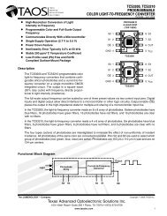
MFRC522 Contactless reader IC - NXP.com
MFRC522 Contactless reader IC - NXP.com
MFRC522 Contactless reader IC - NXP.com

You also want an ePaper? Increase the reach of your titles
YUMPU automatically turns print PDFs into web optimized ePapers that Google loves.
<strong>MFRC522</strong><br />
<strong>Contactless</strong> <strong>reader</strong> <strong>IC</strong><br />
Rev. 3.6 — 14 December 2011<br />
112136<br />
Product data sheet<br />
COMPANY PUBL<strong>IC</strong><br />
1. Introduction<br />
2. General description<br />
This document describes the functionality and electrical specifications of the contactless<br />
<strong>reader</strong>/writer <strong>MFRC522</strong>.<br />
Remark: The <strong>MFRC522</strong> supports all variants of the MIFARE Mini, MIFARE 1K,<br />
MIFARE 4K, MIFARE Ultralight, MIFARE DESFire EV1 and MIFARE Plus RF<br />
identification protocols. To aid readability throughout this data sheet, the MIFARE Mini,<br />
MIFARE 1K, MIFARE 4K, MIFARE Ultralight, MIFARE DESFire EV1 and MIFARE Plus<br />
products and protocols have the generic name MIFARE.<br />
The <strong>MFRC522</strong> is a highly integrated <strong>reader</strong>/writer <strong>IC</strong> for contactless <strong>com</strong>munication<br />
at 13.56 MHz. The <strong>MFRC522</strong> <strong>reader</strong> supports ISO/IEC 14443 A/MIFARE mode.<br />
The <strong>MFRC522</strong>’s internal transmitter is able to drive a <strong>reader</strong>/writer antenna designed to<br />
<strong>com</strong>municate with ISO/IEC 14443 A/MIFARE cards and transponders without additional<br />
active circuitry. The receiver module provides a robust and efficient implementation for<br />
demodulating and decoding signals from ISO/IEC 14443 A/MIFARE <strong>com</strong>patible cards and<br />
transponders. The digital module manages the <strong>com</strong>plete ISO/IEC 14443 A framing and<br />
error detection (parity and CRC) functionality.<br />
The <strong>MFRC522</strong> supports MF1xxS20, MF1xxS70 and MF1xxS50 products. The <strong>MFRC522</strong><br />
supports contactless <strong>com</strong>munication and uses MIFARE higher transfer speeds up to<br />
848 kBd in both directions.<br />
The following host interfaces are provided:<br />
• Serial Peripheral Interface (SPI)<br />
• Serial UART (similar to RS232 with voltage levels dependant on pin voltage supply)<br />
• I 2 C-bus interface<br />
2.1 Differences between version 1.0 and 2.0<br />
The <strong>MFRC522</strong> is available in two versions:<br />
• <strong>MFRC522</strong>01HN1, hereafter referred to version 1.0 and<br />
• <strong>MFRC522</strong>02HN1, hereafter referred to version 2.0.<br />
The <strong>MFRC522</strong> version 2.0 is fully <strong>com</strong>patible to version 1.0 and offers in addition the<br />
following features and improvements:
<strong>NXP</strong> Semiconductors<br />
<strong>MFRC522</strong><br />
<strong>Contactless</strong> <strong>reader</strong> <strong>IC</strong><br />
3. Features and benefits<br />
4. Quick reference data<br />
• Increased stability of the <strong>reader</strong> <strong>IC</strong> in rough conditions<br />
• An additional timer prescaler, see Section 8.5.<br />
• A corrected CRC handling when RX Multiple is set to 1<br />
This data sheet version covers both versions of the <strong>MFRC522</strong> and describes the<br />
differences between the versions if applicable.<br />
• Highly integrated analog circuitry to demodulate and decode responses<br />
• Buffered output drivers for connecting an antenna with the minimum number of<br />
external <strong>com</strong>ponents<br />
• Supports ISO/IEC 14443 A/MIFARE<br />
• Typical operating distance in Read/Write mode up to 50 mm depending on the<br />
antenna size and tuning<br />
• Supports MF1xxS20, MF1xxS70 and MF1xxS50 encryption in Read/Write mode<br />
• Supports ISO/IEC 14443 A higher transfer speed <strong>com</strong>munication up to 848 kBd<br />
• Supports MFIN/MFOUT<br />
• Additional internal power supply to the smart card <strong>IC</strong> connected via MFIN/MFOUT<br />
• Supported host interfaces<br />
SPI up to 10 Mbit/s<br />
I 2 C-bus interface up to 400 kBd in Fast mode, up to 3400 kBd in High-speed mode<br />
RS232 Serial UART up to 1228.8 kBd, with voltage levels dependant on pin<br />
voltage supply<br />
• FIFO buffer handles 64 byte send and receive<br />
• Flexible interrupt modes<br />
• Hard reset with low power function<br />
• Power-down by software mode<br />
• Programmable timer<br />
• Internal oscillator for connection to 27.12 MHz quartz crystal<br />
• 2.5 V to 3.3 V power supply<br />
• CRC coprocessor<br />
• Programmable I/O pins<br />
• Internal self-test<br />
Table 1. Quick reference data<br />
Symbol Parameter Conditions Min Typ Max Unit<br />
V DDA analog supply voltage V DD(PVDD) V DDA = V DDD = V DD(TVDD) ;<br />
[1][2]<br />
2.5 3.3 3.6 V<br />
V DDD digital supply voltage<br />
V SSA =V SSD =V SS(PVSS) =V SS(TVSS) =0V<br />
2.5 3.3 3.6 V<br />
V DD(TVDD) TVDD supply voltage 2.5 3.3 3.6 V<br />
V DD(PVDD) PVDD supply voltage<br />
[3]<br />
1.6 1.8 3.6 V<br />
V DD(SVDD) SVDD supply voltage V SSA =V SSD =V SS(PVSS) =V SS(TVSS) = 0 V 1.6 - 3.6 V<br />
<strong>MFRC522</strong> All information provided in this document is subject to legal disclaimers. © <strong>NXP</strong> B.V. 2011. All rights reserved.<br />
Product data sheet<br />
COMPANY PUBL<strong>IC</strong><br />
Rev. 3.6 — 14 December 2011<br />
112136 2 of 94
<strong>NXP</strong> Semiconductors<br />
<strong>MFRC522</strong><br />
<strong>Contactless</strong> <strong>reader</strong> <strong>IC</strong><br />
Table 1. Quick reference data …continued<br />
Symbol Parameter Conditions Min Typ Max Unit<br />
I pd power-down current V DDA =V DDD = V DD(TVDD) =V DD(PVDD) =3V<br />
hard power-down; pin NRSTPD set LOW<br />
[4]<br />
- - 5 A<br />
soft power-down; RF level detector on<br />
[4]<br />
- - 10 A<br />
I DDD digital supply current pin DVDD; V DDD =3V - 6.5 9 mA<br />
I DDA analog supply current pin AVDD; V DDA = 3 V, CommandReg register’s - 7 10 mA<br />
RcvOff bit = 0<br />
pin AVDD; receiver switched off; V DDA =3V,<br />
- 3 5 mA<br />
CommandReg register’s RcvOff bit = 1<br />
I DD(PVDD) PVDD supply current pin PVDD<br />
[5]<br />
- - 40 mA<br />
I DD(TVDD) TVDD supply current pin TVDD; continuous wave<br />
[6][7][8]<br />
- 60 100 mA<br />
T amb ambient temperature HVQFN32 25 - +85 C<br />
[1] Supply voltages below 3 V reduce the performance in, for example, the achievable operating distance.<br />
[2] V DDA , V DDD and V DD(TVDD) must always be the same voltage.<br />
[3] V DD(PVDD) must always be the same or lower voltage than V DDD .<br />
[4] I pd is the total current for all supplies.<br />
[5] I DD(PVDD) depends on the overall load at the digital pins.<br />
[6] I DD(TVDD) depends on V DD(TVDD) and the external circuit connected to pins TX1 and TX2.<br />
[7] During typical circuit operation, the overall current is below 100 mA.<br />
[8] Typical value using a <strong>com</strong>plementary driver configuration and an antenna matched to 40 between pins TX1 and TX2 at 13.56 MHz.<br />
5. Ordering information<br />
Table 2. Ordering information<br />
Type number<br />
Package<br />
Name Description Version<br />
<strong>MFRC522</strong>01HN1/TRAYB [1] HVQFN32 plastic thermal enhanced very thin quad flat package; no leads; SOT617-1<br />
32 terminal; body 5 5 0.85 mm<br />
<strong>MFRC522</strong>01HN1/TRAYBM [2] HVQFN32 plastic thermal enhanced very thin quad flat package; no leads; SOT617-1<br />
32 terminal; body 5 5 0.85 mm<br />
<strong>MFRC522</strong>02HN1/TRAYB [1] HVQFN32 plastic thermal enhanced very thin quad flat package; no leads; SOT617-1<br />
32 terminal; body 5 5 0.85 mm<br />
<strong>MFRC522</strong>02HN1/TRAYBM [2] HVQFN32 plastic thermal enhanced very thin quad flat package; no leads;<br />
32 terminal; body 5 5 0.85 mm<br />
SOT617-1<br />
[1] Delivered in one tray.<br />
[2] Delivered in five trays.<br />
<strong>MFRC522</strong> All information provided in this document is subject to legal disclaimers. © <strong>NXP</strong> B.V. 2011. All rights reserved.<br />
Product data sheet<br />
COMPANY PUBL<strong>IC</strong><br />
Rev. 3.6 — 14 December 2011<br />
112136 3 of 94
<strong>NXP</strong> Semiconductors<br />
<strong>MFRC522</strong><br />
<strong>Contactless</strong> <strong>reader</strong> <strong>IC</strong><br />
6. Block diagram<br />
The analog interface handles the modulation and demodulation of the analog signals.<br />
The contactless UART manages the protocol requirements for the <strong>com</strong>munication<br />
protocols in cooperation with the host. The FIFO buffer ensures fast and convenient data<br />
transfer to and from the host and the contactless UART and vice versa.<br />
Various host interfaces are implemented to meet different customer requirements.<br />
REGISTER BANK<br />
ANTENNA<br />
ANALOG<br />
INTERFACE<br />
CONTACTLESS<br />
UART<br />
FIFO<br />
BUFFER<br />
SERIAL UART<br />
SPI<br />
I 2 C-BUS<br />
HOST<br />
001aaj627<br />
Fig 1.<br />
Simplified block diagram of the <strong>MFRC522</strong><br />
<strong>MFRC522</strong> All information provided in this document is subject to legal disclaimers. © <strong>NXP</strong> B.V. 2011. All rights reserved.<br />
Product data sheet<br />
COMPANY PUBL<strong>IC</strong><br />
Rev. 3.6 — 14 December 2011<br />
112136 4 of 94
<strong>NXP</strong> Semiconductors<br />
<strong>MFRC522</strong><br />
<strong>Contactless</strong> <strong>reader</strong> <strong>IC</strong><br />
SDA/NSS/RX EA I2C<br />
D6/ADR_0/<br />
D2/ADR_4 D4/ADR_2 MOSI/MX<br />
D5/ADR_1/ D7/SCL/<br />
D1/ADR_5 D3/ADR_3 SCK/DTRQ MISO/TX<br />
PVDD<br />
PVSS<br />
24 32 1<br />
FIFO CONTROL<br />
25 26 27 28 29 30 31<br />
SPI, UART, I 2 C-BUS INTERFACE CONTROL<br />
STATE MACHINE<br />
2<br />
5<br />
VOLTAGE<br />
MONITOR<br />
AND<br />
POWER ON<br />
DETECT<br />
3<br />
4<br />
15<br />
18<br />
DVDD<br />
DVSS<br />
AVDD<br />
AVSS<br />
64-BYTE FIFO<br />
BUFFER<br />
COMMAND REGISTER<br />
RESET<br />
CONTROL<br />
CONTROL REGISTER<br />
BANK<br />
PROGRAMABLE TIMER<br />
INTERRUPT CONTROL<br />
POWER-DOWN<br />
CONTROL<br />
6<br />
23<br />
NRSTPD<br />
IRQ<br />
MIFARE CLASS<strong>IC</strong> UNIT<br />
CRC16<br />
GENERATION AND CHECK<br />
RANDOM NUMBER<br />
GENERATOR<br />
PARALLEL/SERIAL<br />
CONVERTER<br />
BIT COUNTER<br />
PARITY GENERATION AND CHECK<br />
FRAME GENERATION AND CHECK<br />
BIT DECODING<br />
BIT ENCODING<br />
SERIAL DATA SWITCH<br />
7<br />
8<br />
9<br />
MFIN<br />
MFOUT<br />
SVDD<br />
AMPLITUDE<br />
RATING<br />
REFERENCE<br />
VOLTAGE<br />
ANALOG TEST<br />
MULTIPLEXOR<br />
AND<br />
DIGITAL TO<br />
ANALOG<br />
CONVERTER<br />
I-CHANNEL<br />
AMPLIFIER<br />
I-CHANNEL<br />
DEMODULATOR<br />
ANALOG TO DIGITAL<br />
CONVERTER<br />
Q-CHANNEL<br />
AMPLIFIER<br />
Q-CHANNEL<br />
DEMODULATOR<br />
CLOCK<br />
GENERATION,<br />
FILTERING AND<br />
DISTRIBUTION<br />
Q-CLOCK<br />
GENERATION<br />
OSCILLATOR<br />
TEMPERATURE<br />
SENSOR<br />
TRANSMITTER CONTROL<br />
21<br />
22<br />
OSCIN<br />
OSCOUT<br />
16 19 20 17 10, 14 11 13 12<br />
VMID AUX1 AUX2 RX TVSS TX1 TX2 TVDD<br />
001aak602<br />
Fig 2.<br />
Detailed block diagram of the <strong>MFRC522</strong><br />
<strong>MFRC522</strong> All information provided in this document is subject to legal disclaimers. © <strong>NXP</strong> B.V. 2011. All rights reserved.<br />
Product data sheet<br />
COMPANY PUBL<strong>IC</strong><br />
Rev. 3.6 — 14 December 2011<br />
112136 5 of 94
<strong>NXP</strong> Semiconductors<br />
<strong>MFRC522</strong><br />
<strong>Contactless</strong> <strong>reader</strong> <strong>IC</strong><br />
7. Pinning information<br />
EA<br />
D7/SCL/MISO/TX<br />
D6/ADR_0/MOSI/MX<br />
D5/ADR_1/SCK/DTRQ<br />
D4/ADR_2<br />
D3/ADR_3<br />
D2/ADR_4<br />
D1/ADR_5<br />
I2C<br />
PVDD<br />
DVDD<br />
DVSS<br />
PVSS<br />
NRSTPD<br />
MFIN<br />
MFOUT<br />
1 24<br />
2 23<br />
3 22<br />
4 21<br />
<strong>MFRC522</strong><br />
5 20<br />
6 19<br />
7 18<br />
8 17<br />
SDA/NSS/RX<br />
IRQ<br />
OSCOUT<br />
OSCIN<br />
AUX2<br />
AUX1<br />
AVSS<br />
RX<br />
SVDD<br />
TVSS<br />
TX1<br />
TVDD<br />
TX2<br />
TVSS<br />
AVDD<br />
VMID<br />
9<br />
10<br />
11<br />
12<br />
13<br />
14<br />
15<br />
16<br />
32<br />
31<br />
30<br />
29<br />
28<br />
27<br />
26<br />
25<br />
Transparent top view<br />
001aaj819<br />
Fig 3.<br />
Pinning configuration HVQFN32 (SOT617-1)<br />
7.1 Pin description<br />
Table 3. Pin description<br />
Pin Symbol Type [1] Description<br />
1 I2C I I 2 C-bus enable input [2]<br />
2 PVDD P pin power supply<br />
3 DVDD P digital power supply<br />
4 DVSS G digital ground [3]<br />
5 PVSS G pin power supply ground<br />
6 NRSTPD I reset and power-down input:<br />
power-down: enabled when LOW; internal current sinks are switched off, the oscillator<br />
is inhibited and the input pins are disconnected from the outside world<br />
reset: enabled by a positive edge<br />
7 MFIN I MIFARE signal input<br />
8 MFOUT O MIFARE signal output<br />
9 SVDD P MFIN and MFOUT pin power supply<br />
10 TVSS G transmitter output stage 1 ground<br />
11 TX1 O transmitter 1 modulated 13.56 MHz energy carrier output<br />
12 TVDD P transmitter power supply: supplies the output stage of transmitters 1 and 2<br />
13 TX2 O transmitter 2 modulated 13.56 MHz energy carrier output<br />
14 TVSS G transmitter output stage 2 ground<br />
15 AVDD P analog power supply<br />
<strong>MFRC522</strong> All information provided in this document is subject to legal disclaimers. © <strong>NXP</strong> B.V. 2011. All rights reserved.<br />
Product data sheet<br />
COMPANY PUBL<strong>IC</strong><br />
Rev. 3.6 — 14 December 2011<br />
112136 6 of 94
<strong>NXP</strong> Semiconductors<br />
<strong>MFRC522</strong><br />
<strong>Contactless</strong> <strong>reader</strong> <strong>IC</strong><br />
Table 3. Pin description …continued<br />
Pin Symbol Type [1] Description<br />
16 VMID P internal reference voltage<br />
17 RX I RF signal input<br />
18 AVSS G analog ground<br />
19 AUX1 O auxiliary outputs for test purposes<br />
20 AUX2 O auxiliary outputs for test purposes<br />
21 OSCIN I crystal oscillator inverting amplifier input; also the input for an externally generated clock<br />
(f clk = 27.12 MHz)<br />
22 OSCOUT O crystal oscillator inverting amplifier output<br />
23 IRQ O interrupt request output: indicates an interrupt event<br />
24 SDA I/O I 2 C-bus serial data line input/output [2]<br />
NSS I SPI signal input [2]<br />
RX I UART address input [2]<br />
25 D1 I/O test port [2]<br />
ADR_5 I/O I 2 C-bus address 5 input [2]<br />
26 D2 I/O test port<br />
ADR_4 I I 2 C-bus address 4 input [2]<br />
27 D3 I/O test port<br />
ADR_3 I I 2 C-bus address 3 input [2]<br />
28 D4 I/O test port<br />
ADR_2 I I 2 C-bus address 2 input [2]<br />
29 D5 I/O test port<br />
ADR_1 I I 2 C-bus address 1 input [2]<br />
SCK I SPI serial clock input [2]<br />
DTRQ O UART request to send output to microcontroller [2]<br />
30 D6 I/O test port<br />
ADR_0 I I 2 C-bus address 0 input [2]<br />
MOSI I/O SPI master out, slave in [2]<br />
MX O UART output to microcontroller [2]<br />
31 D7 I/O test port<br />
SCL I/O I 2 C-bus clock input/output [2]<br />
MISO I/O SPI master in, slave out [2]<br />
TX O UART data output to microcontroller [2]<br />
32 EA I external address input for coding I 2 C-bus address [2]<br />
[1] Pin types: I = Input, O = Output, I/O = Input/Output, P = Power and G = Ground.<br />
[2] The pin functionality of these pins is explained in Section 8.1 “Digital interfaces”.<br />
[3] Connection of heatsink pad on package bottom side is not necessary. Optional connection to pin DVSS is possible.<br />
<strong>MFRC522</strong> All information provided in this document is subject to legal disclaimers. © <strong>NXP</strong> B.V. 2011. All rights reserved.<br />
Product data sheet<br />
COMPANY PUBL<strong>IC</strong><br />
Rev. 3.6 — 14 December 2011<br />
112136 7 of 94
<strong>NXP</strong> Semiconductors<br />
<strong>MFRC522</strong><br />
<strong>Contactless</strong> <strong>reader</strong> <strong>IC</strong><br />
8. Functional description<br />
The <strong>MFRC522</strong> transmission module supports the Read/Write mode for<br />
ISO/IEC 14443 A/MIFARE using various transfer speeds and modulation protocols.<br />
BATTERY<br />
M<strong>IC</strong>ROCONTROLLER<br />
<strong>reader</strong>/writer<br />
<strong>MFRC522</strong><br />
ISO/IEC 14443 A CARD<br />
contactless card<br />
001aak583<br />
Fig 4.<br />
<strong>MFRC522</strong> Read/Write mode<br />
The physical level <strong>com</strong>munication is shown in Figure 5.<br />
ISO/IEC 14443 A<br />
READER<br />
<strong>MFRC522</strong><br />
(1)<br />
(2)<br />
ISO/IEC 14443 A CARD<br />
001aak584<br />
(1) Reader to card 100 % ASK, Miller encoded, transfer speed 106 kBd to 848 kBd.<br />
(2) Card to <strong>reader</strong> subcarrier load modulation, Manchester encoded or BPSK, transfer speed 106 kBd<br />
to 848 kBd.<br />
Fig 5. ISO/IEC 14443 A/MIFARE Read/Write mode <strong>com</strong>munication diagram<br />
The physical parameters are described in Table 4.<br />
Table 4. Communication overview for ISO/IEC 14443 A/MIFARE <strong>reader</strong>/writer<br />
Communication Signal type Transfer speed<br />
direction<br />
106 kBd 212 kBd 424 kBd 848 kBd<br />
Reader to card (send<br />
data from the<br />
<strong>MFRC522</strong> to a card)<br />
<strong>reader</strong> side<br />
modulation<br />
100 % ASK 100 % ASK 100 % ASK 100 % ASK<br />
Card to <strong>reader</strong><br />
(<strong>MFRC522</strong> receives<br />
data from a card)<br />
bit encoding<br />
modified Miller<br />
encoding<br />
modified Miller<br />
encoding<br />
modified Miller<br />
encoding<br />
modified Miller<br />
encoding<br />
bit length 128 (13.56 s) 64 (13.56 s) 32 (13.56 s) 16 (13.56 s)<br />
card side<br />
modulation<br />
subcarrier<br />
frequency<br />
bit encoding<br />
subcarrier load<br />
modulation<br />
subcarrier load<br />
modulation<br />
subcarrier load<br />
modulation<br />
subcarrier load<br />
modulation<br />
13.56 MHz / 16 13.56 MHz / 16 13.56 MHz / 16 13.56 MHz / 16<br />
Manchester<br />
encoding<br />
BPSK BPSK BPSK<br />
The <strong>MFRC522</strong>’s contactless UART and dedicated external host must manage the<br />
<strong>com</strong>plete ISO/IEC 14443 A/MIFARE protocol. Figure 6 shows the data coding and<br />
framing according to ISO/IEC 14443 A/MIFARE.<br />
<strong>MFRC522</strong> All information provided in this document is subject to legal disclaimers. © <strong>NXP</strong> B.V. 2011. All rights reserved.<br />
Product data sheet<br />
COMPANY PUBL<strong>IC</strong><br />
Rev. 3.6 — 14 December 2011<br />
112136 8 of 94
<strong>NXP</strong> Semiconductors<br />
<strong>MFRC522</strong><br />
<strong>Contactless</strong> <strong>reader</strong> <strong>IC</strong><br />
ISO/IEC 14443 A framing at 106 kBd<br />
start<br />
8-bit data 8-bit data 8-bit data<br />
start bit is 1<br />
odd<br />
parity<br />
odd<br />
parity<br />
odd<br />
parity<br />
ISO/IEC 14443 A framing at 212 kBd, 424 kBd and 848 kBd<br />
start<br />
even<br />
parity<br />
8-bit data 8-bit data 8-bit data<br />
start bit is 0<br />
odd<br />
parity<br />
odd<br />
parity<br />
burst of 32<br />
subcarrier clocks<br />
even parity at the<br />
end of the frame<br />
001aak585<br />
Fig 6.<br />
Data coding and framing according to ISO/IEC 14443 A<br />
The internal CRC coprocessor calculates the CRC value based on ISO/IEC 14443 A<br />
part 3 and handles parity generation internally according to the transfer speed. Automatic<br />
parity generation can be switched off using the MfRxReg register’s ParityDisable bit.<br />
8.1 Digital interfaces<br />
8.1.1 Automatic microcontroller interface detection<br />
The <strong>MFRC522</strong> supports direct interfacing of hosts using SPI, I 2 C-bus or serial UART<br />
interfaces. The <strong>MFRC522</strong> resets its interface and checks the current host interface type<br />
automatically after performing a power-on or hard reset. The <strong>MFRC522</strong> identifies the host<br />
interface by sensing the logic levels on the control pins after the reset phase. This is done<br />
using a <strong>com</strong>bination of fixed pin connections. Table 5 shows the different connection<br />
configurations.<br />
Table 5. Connection protocol for detecting different interface types<br />
Pin<br />
Interface type<br />
UART (input) SPI (output) I 2 C-bus (I/O)<br />
SDA RX NSS SDA<br />
I2C 0 0 1<br />
EA 0 1 EA<br />
D7 TX MISO SCL<br />
D6 MX MOSI ADR_0<br />
D5 DTRQ SCK ADR_1<br />
D4 - - ADR_2<br />
D3 - - ADR_3<br />
D2 - - ADR_4<br />
D1 - - ADR_5<br />
<strong>MFRC522</strong> All information provided in this document is subject to legal disclaimers. © <strong>NXP</strong> B.V. 2011. All rights reserved.<br />
Product data sheet<br />
COMPANY PUBL<strong>IC</strong><br />
Rev. 3.6 — 14 December 2011<br />
112136 9 of 94
<strong>NXP</strong> Semiconductors<br />
<strong>MFRC522</strong><br />
<strong>Contactless</strong> <strong>reader</strong> <strong>IC</strong><br />
8.1.2 Serial Peripheral Interface<br />
A serial peripheral interface (SPI <strong>com</strong>patible) is supported to enable high-speed<br />
<strong>com</strong>munication to the host. The interface can handle data speeds up to 10 Mbit/s. When<br />
<strong>com</strong>municating with a host, the <strong>MFRC522</strong> acts as a slave, receiving data from the<br />
external host for register settings, sending and receiving data relevant for RF interface<br />
<strong>com</strong>munication.<br />
An interface <strong>com</strong>patible with SPI enables high-speed serial <strong>com</strong>munication between the<br />
<strong>MFRC522</strong> and a microcontroller. The implemented interface is in accordance with the SPI<br />
standard.<br />
The timing specification is given in Section 14.1 on page 77.<br />
<strong>MFRC522</strong><br />
SCK<br />
MOSI<br />
MISO<br />
NSS<br />
SCK<br />
MOSI<br />
MISO<br />
NSS<br />
001aak586<br />
Fig 7.<br />
SPI connection to host<br />
The <strong>MFRC522</strong> acts as a slave during SPI <strong>com</strong>munication. The SPI clock signal SCK must<br />
be generated by the master. Data <strong>com</strong>munication from the master to the slave uses the<br />
MOSI line. The MISO line is used to send data from the <strong>MFRC522</strong> to the master.<br />
Data bytes on both MOSI and MISO lines are sent with the MSB first. Data on both MOSI<br />
and MISO lines must be stable on the rising edge of the clock and can be changed on the<br />
falling edge. Data is provided by the <strong>MFRC522</strong> on the falling clock edge and is stable<br />
during the rising clock edge.<br />
8.1.2.1 SPI read data<br />
Reading data using SPI requires the byte order shown in Table 6 to be used. It is possible<br />
to read out up to n-data bytes.<br />
The first byte sent defines both the mode and the address.<br />
Table 6. MOSI and MISO byte order<br />
Line Byte 0 Byte 1 Byte 2 To Byte n Byte n + 1<br />
MOSI address 0 address 1 address 2 ... address n 00<br />
MISO X [1] data 0 data 1 ... data n 1 data n<br />
[1] X = Do not care.<br />
Remark: The MSB must be sent first.<br />
<strong>MFRC522</strong> All information provided in this document is subject to legal disclaimers. © <strong>NXP</strong> B.V. 2011. All rights reserved.<br />
Product data sheet<br />
COMPANY PUBL<strong>IC</strong><br />
Rev. 3.6 — 14 December 2011<br />
112136 10 of 94
<strong>NXP</strong> Semiconductors<br />
<strong>MFRC522</strong><br />
<strong>Contactless</strong> <strong>reader</strong> <strong>IC</strong><br />
8.1.2.2 SPI write data<br />
To write data to the <strong>MFRC522</strong> using SPI requires the byte order shown in Table 7. It is<br />
possible to write up to n data bytes by only sending one address byte.<br />
The first send byte defines both the mode and the address byte.<br />
Table 7. MOSI and MISO byte order<br />
Line Byte 0 Byte 1 Byte 2 To Byte n Byte n + 1<br />
MOSI address 0 data 0 data 1 ... data n 1 data n<br />
MISO X [1] X [1] X [1] ... X [1] X [1]<br />
[1] X = Do not care.<br />
Remark: The MSB must be sent first.<br />
8.1.2.3 SPI address byte<br />
The address byte must meet the following format.<br />
The MSB of the first byte defines the mode used. To read data from the <strong>MFRC522</strong> the<br />
MSB is set to logic 1. To write data to the <strong>MFRC522</strong> the MSB must be set to logic 0. Bits 6<br />
to 1 define the address and the LSB is set to logic 0.<br />
Table 8. Address byte 0 register; address MOSI<br />
7 (MSB) 6 5 4 3 2 1 0 (LSB)<br />
1 = read<br />
0 = write<br />
address 0<br />
8.1.3 UART interface<br />
8.1.3.1 Connection to a host<br />
RX<br />
TX<br />
DTRQ<br />
MX<br />
<strong>MFRC522</strong><br />
RX<br />
TX<br />
DTRQ<br />
MX<br />
001aak587<br />
Fig 8.<br />
UART connection to microcontrollers<br />
Remark: Signals DTRQ and MX can be disabled by clearing TestPinEnReg register’s<br />
RS232LineEn bit.<br />
<strong>MFRC522</strong> All information provided in this document is subject to legal disclaimers. © <strong>NXP</strong> B.V. 2011. All rights reserved.<br />
Product data sheet<br />
COMPANY PUBL<strong>IC</strong><br />
Rev. 3.6 — 14 December 2011<br />
112136 11 of 94
<strong>NXP</strong> Semiconductors<br />
<strong>MFRC522</strong><br />
<strong>Contactless</strong> <strong>reader</strong> <strong>IC</strong><br />
8.1.3.2 Selectable UART transfer speeds<br />
The internal UART interface is <strong>com</strong>patible with an RS232 serial interface.<br />
The default transfer speed is 9.6 kBd. To change the transfer speed, the host controller<br />
must write a value for the new transfer speed to the SerialSpeedReg register. Bits<br />
BR_T0[2:0] and BR_T1[4:0] define the factors for setting the transfer speed in the<br />
SerialSpeedReg register.<br />
The BR_T0[2:0] and BR_T1[4:0] settings are described in Table 9. Examples of different<br />
transfer speeds and the relevant register settings are given in Table 10.<br />
Table 9. BR_T0 and BR_T1 settings<br />
BR_Tn Bit 0 Bit 1 Bit 2 Bit 3 Bit 4 Bit 5 Bit 6 Bit 7<br />
BR_T0 factor 1 1 2 4 8 16 32 64<br />
BR_T1 range 1 to 32 33 to 64 33 to 64 33 to 64 33 to 64 33 to 64 33 to 64 33 to 64<br />
Table 10. Selectable UART transfer speeds<br />
Transfer speed (kBd) SerialSpeedReg value Transfer speed accuracy<br />
Decimal Hexadecimal<br />
(%) [1]<br />
7.2 250 FAh 0.25<br />
9.6 235 EBh 0.32<br />
14.4 218 DAh 0.25<br />
19.2 203 CBh 0.32<br />
38.4 171 ABh 0.32<br />
57.6 154 9Ah 0.25<br />
115.2 122 7Ah 0.25<br />
128 116 74h 0.06<br />
230.4 90 5Ah 0.25<br />
460.8 58 3Ah 0.25<br />
921.6 28 1Ch 1.45<br />
1228.8 21 15h 0.32<br />
[1] The resulting transfer speed error is less than 1.5 % for all described transfer speeds.<br />
The selectable transfer speeds shown in Table 10 are calculated according to the<br />
following equations:<br />
If BR_T0[2:0] = 0:<br />
transfer speed<br />
=<br />
27.12 10 6<br />
-------------------------------<br />
BR_T0 + 1<br />
(1)<br />
If BR_T0[2:0] > 0:<br />
<br />
<br />
27.12 10<br />
transfer speed<br />
6 <br />
= ----------------------------------<br />
<br />
BR_T1 + 33<br />
---------------------------------- <br />
– <br />
2 BR_T0 1<br />
(2)<br />
<strong>MFRC522</strong> All information provided in this document is subject to legal disclaimers. © <strong>NXP</strong> B.V. 2011. All rights reserved.<br />
Product data sheet<br />
COMPANY PUBL<strong>IC</strong><br />
Remark: Transfer speeds above 1228.8 kBd are not supported.<br />
Rev. 3.6 — 14 December 2011<br />
112136 12 of 94
<strong>NXP</strong> Semiconductors<br />
<strong>MFRC522</strong><br />
<strong>Contactless</strong> <strong>reader</strong> <strong>IC</strong><br />
8.1.3.3 UART framing<br />
Table 11.<br />
UART framing<br />
Bit Length Value<br />
Start 1-bit 0<br />
Data 8 bits data<br />
Stop 1-bit 1<br />
Remark: The LSB for data and address bytes must be sent first. No parity bit is used<br />
during transmission.<br />
Read data: To read data using the UART interface, the flow shown in Table 12 must be<br />
used. The first byte sent defines both the mode and the address.<br />
Table 12. Read data byte order<br />
Pin Byte 0 Byte 1<br />
RX (pin 24) address -<br />
TX (pin 31) - data 0<br />
ADDRESS<br />
RX<br />
SA<br />
A0 A1 A2 A3 A4 A5 (1) R/W SO<br />
DATA<br />
TX<br />
SA D0 D1 D2 D3 D4 D5 D6 D7 SO<br />
MX<br />
DTRQ<br />
001aak588<br />
(1) Reserved.<br />
Fig 9. UART read data timing diagram<br />
Write data: To write data to the <strong>MFRC522</strong> using the UART interface, the structure shown<br />
in Table 13 must be used.<br />
The first byte sent defines both the mode and the address.<br />
<strong>MFRC522</strong> All information provided in this document is subject to legal disclaimers. © <strong>NXP</strong> B.V. 2011. All rights reserved.<br />
Product data sheet<br />
COMPANY PUBL<strong>IC</strong><br />
Rev. 3.6 — 14 December 2011<br />
112136 13 of 94
<strong>NXP</strong> Semiconductors<br />
<strong>MFRC522</strong><br />
<strong>Contactless</strong> <strong>reader</strong> <strong>IC</strong><br />
Table 13. Write data byte order<br />
Pin Byte 0 Byte 1<br />
RX (pin 24) address 0 data 0<br />
TX (pin 31) - address 0<br />
<strong>MFRC522</strong> All information provided in this document is subject to legal disclaimers. © <strong>NXP</strong> B.V. 2011. All rights reserved.<br />
Product data sheet<br />
COMPANY PUBL<strong>IC</strong><br />
Rev. 3.6 — 14 December 2011<br />
112136 14 of 94
Product data sheet<br />
COMPANY PUBL<strong>IC</strong><br />
Rev. 3.6 — 14 December 2011<br />
112136 15 of 94<br />
<strong>MFRC522</strong> All information provided in this document is subject to legal disclaimers. © <strong>NXP</strong> B.V. 2011. All rights reserved.<br />
Fig 10.<br />
RX<br />
TX<br />
MX<br />
DTRQ<br />
xxxxxxxxxxxxxxxxxxxxx xxxxxxxxxxxxxxxxxxxxxxxxxx xxxxxxx x x x xxxxxxxxxxxxxxxxxxxxxxxxxxxxxx xxxxxxxxxxxxxxxxxxx xx xx xxxxx<br />
xxxxxxxxxxxxxxxxxxxxxxxxxxx xxxxxxxxxxxxxxxxxxx xxxxxx xxxxxxxxxxxxxxxxxxxxxxxxxxxxxxxxxxx xxxxxxxxxxxx x x<br />
xxxxxxxxxxxxxxxxxxxxx xxxxxxxxxxxxxxxxxxxxxxxxxxxxxx xxxxx xxxxxxxxxxxxxxxxxxxxxxxxxxxxxxxxxxxxxxxxxxxxxxxxxx xxxxxxxx<br />
xxxxxxxxxxxxxxxxxxxxxxxxx xxxxxxxxxxxxxxxxxxxx xxx<br />
(1) Reserved.<br />
SA<br />
ADDRESS<br />
A0 A1 A2 A3 A4 A5 (1) R/W SO SA D0 D1 D2 D3 D4 D5 D6 D7 SO<br />
UART write data timing diagram<br />
ADDRESS<br />
SA A0 A1 A2 A3 A4 A5 (1) R/W SO<br />
Remark: The data byte can be sent directly after the address byte on pin RX.<br />
Address byte: The address byte has to meet the following format:<br />
001aak589<br />
The MSB of the first byte sets the mode used. To read data from the <strong>MFRC522</strong>, the MSB is set to logic 1. To write data to the<br />
<strong>MFRC522</strong> the MSB is set to logic 0. Bit 6 is reserved for future use, and bits 5 to 0 define the address; see Table 14.<br />
DATA<br />
<strong>Contactless</strong> <strong>reader</strong> <strong>IC</strong><br />
<strong>NXP</strong> Semiconductors <strong>MFRC522</strong>
<strong>NXP</strong> Semiconductors<br />
<strong>MFRC522</strong><br />
<strong>Contactless</strong> <strong>reader</strong> <strong>IC</strong><br />
Table 14. Address byte 0 register; address MOSI<br />
7 (MSB) 6 5 4 3 2 1 0 (LSB)<br />
1 = read<br />
0 = write<br />
reserved address<br />
8.1.4 I 2 C-bus interface<br />
An I 2 C-bus (Inter-<strong>IC</strong>) interface is supported to enable a low-cost, low pin count serial bus<br />
interface to the host. The I 2 C-bus interface is implemented according to<br />
<strong>NXP</strong> Semiconductors’ I 2 C-bus interface specification, rev. 2.1, January 2000. The<br />
interface can only act in Slave mode. Therefore the <strong>MFRC522</strong> does not implement clock<br />
generation or access arbitration.<br />
PULL-UP<br />
NETWORK<br />
PULL-UP<br />
NETWORK<br />
SDA<br />
<strong>MFRC522</strong><br />
M<strong>IC</strong>ROCONTROLLER<br />
SCL<br />
CONFIGURATION<br />
WIRING<br />
I2C<br />
EA<br />
ADR_[5:0]<br />
001aak590<br />
Fig 11.<br />
I 2 C-bus interface<br />
The <strong>MFRC522</strong> can act either as a slave receiver or slave transmitter in Standard mode,<br />
Fast mode and High-speed mode.<br />
SDA is a bidirectional line connected to a positive supply voltage using a current source or<br />
a pull-up resistor. Both SDA and SCL lines are set HIGH when data is not transmitted. The<br />
<strong>MFRC522</strong> has a 3-state output stage to perform the wired-AND function. Data on the<br />
I 2 C-bus can be transferred at data rates of up to 100 kBd in Standard mode, up to<br />
400 kBd in Fast mode or up to 3.4 Mbit/s in High-speed mode.<br />
If the I 2 C-bus interface is selected, spike suppression is activated on lines SCL and SDA<br />
as defined in the I 2 C-bus interface specification.<br />
See Table 155 on page 78 for timing requirements.<br />
<strong>MFRC522</strong> All information provided in this document is subject to legal disclaimers. © <strong>NXP</strong> B.V. 2011. All rights reserved.<br />
Product data sheet<br />
COMPANY PUBL<strong>IC</strong><br />
Rev. 3.6 — 14 December 2011<br />
112136 16 of 94
<strong>NXP</strong> Semiconductors<br />
<strong>MFRC522</strong><br />
<strong>Contactless</strong> <strong>reader</strong> <strong>IC</strong><br />
8.1.4.1 Data validity<br />
Data on the SDA line must be stable during the HIGH clock period. The HIGH or LOW<br />
state of the data line must only change when the clock signal on SCL is LOW.<br />
SDA<br />
SCL<br />
data line<br />
stable;<br />
data valid<br />
change<br />
of data<br />
allowed<br />
mbc621<br />
Fig 12.<br />
Bit transfer on the I 2 C-bus<br />
8.1.4.2 START and STOP conditions<br />
To manage the data transfer on the I 2 C-bus, unique START (S) and STOP (P) conditions<br />
are defined.<br />
• A START condition is defined with a HIGH-to-LOW transition on the SDA line while<br />
SCL is HIGH.<br />
• A STOP condition is defined with a LOW-to-HIGH transition on the SDA line while<br />
SCL is HIGH.<br />
The I 2 C-bus master always generates the START and STOP conditions. The bus is busy<br />
after the START condition. The bus is free again a certain time after the STOP condition.<br />
The bus stays busy if a repeated START (Sr) is generated instead of a STOP condition.<br />
The START (S) and repeated START (Sr) conditions are functionally identical. Therefore,<br />
S is used as a generic term to represent both the START (S) and repeated START (Sr)<br />
conditions.<br />
SDA<br />
SDA<br />
SCL<br />
S<br />
P<br />
SCL<br />
START condition<br />
STOP condition<br />
mbc622<br />
Fig 13.<br />
START and STOP conditions<br />
8.1.4.3 Byte format<br />
Each byte must be followed by an acknowledge bit. Data is transferred with the MSB first;<br />
see Figure 16. The number of transmitted bytes during one data transfer is unrestricted<br />
but must meet the read/write cycle format.<br />
<strong>MFRC522</strong> All information provided in this document is subject to legal disclaimers. © <strong>NXP</strong> B.V. 2011. All rights reserved.<br />
Product data sheet<br />
COMPANY PUBL<strong>IC</strong><br />
Rev. 3.6 — 14 December 2011<br />
112136 17 of 94
<strong>NXP</strong> Semiconductors<br />
<strong>MFRC522</strong><br />
<strong>Contactless</strong> <strong>reader</strong> <strong>IC</strong><br />
8.1.4.4 Acknowledge<br />
An acknowledge must be sent at the end of one data byte. The acknowledge-related clock<br />
pulse is generated by the master. The transmitter of data, either master or slave, releases<br />
the SDA line (HIGH) during the acknowledge clock pulse. The receiver pulls down the<br />
SDA line during the acknowledge clock pulse so that it remains stable LOW during the<br />
HIGH period of this clock pulse.<br />
The master can then generate either a STOP (P) condition to stop the transfer or a<br />
repeated START (Sr) condition to start a new transfer.<br />
A master-receiver indicates the end of data to the slave-transmitter by not generating an<br />
acknowledge on the last byte that was clocked out by the slave. The slave-transmitter<br />
releases the data line to allow the master to generate a STOP (P) or repeated START (Sr)<br />
condition.<br />
data output<br />
by transmitter<br />
data output<br />
by receiver<br />
not acknowledge<br />
acknowledge<br />
SCL from<br />
master<br />
S<br />
START<br />
condition<br />
1<br />
2<br />
8<br />
9<br />
clock pulse for<br />
acknowledgement<br />
mbc602<br />
Fig 14.<br />
Acknowledge on the I 2 C-bus<br />
P<br />
SDA<br />
MSB<br />
acknowledgement<br />
signal from slave<br />
acknowledgement<br />
signal from receiver<br />
Sr<br />
byte <strong>com</strong>plete,<br />
interrupt within slave<br />
clock line held LOW while<br />
interrupts are serviced<br />
SCL<br />
S<br />
or<br />
Sr<br />
START or<br />
repeated START<br />
condition<br />
1 2<br />
7 8<br />
9<br />
ACK<br />
1 2 3 - 8 9<br />
ACK<br />
Sr<br />
or<br />
P<br />
STOP or<br />
repeated START<br />
condition<br />
msc608<br />
Fig 15.<br />
Data transfer on the I 2 C-bus<br />
<strong>MFRC522</strong> All information provided in this document is subject to legal disclaimers. © <strong>NXP</strong> B.V. 2011. All rights reserved.<br />
Product data sheet<br />
COMPANY PUBL<strong>IC</strong><br />
Rev. 3.6 — 14 December 2011<br />
112136 18 of 94
<strong>NXP</strong> Semiconductors<br />
<strong>MFRC522</strong><br />
<strong>Contactless</strong> <strong>reader</strong> <strong>IC</strong><br />
8.1.4.5 7-Bit addressing<br />
During the I 2 C-bus address procedure, the first byte after the START condition is used to<br />
determine which slave will be selected by the master.<br />
Several address numbers are reserved. During device configuration, the designer must<br />
ensure that collisions with these reserved addresses cannot occur. Check the I 2 C-bus<br />
specification for a <strong>com</strong>plete list of reserved addresses.<br />
The I 2 C-bus address specification is dependent on the definition of pin EA. Immediately<br />
after releasing pin NRSTPD or after a power-on reset, the device defines the I 2 C-bus<br />
address according to pin EA.<br />
If pin EA is set LOW, the upper 4 bits of the device bus address are reserved by<br />
<strong>NXP</strong> Semiconductors and set to 0101b for all <strong>MFRC522</strong> devices. The remaining 3 bits<br />
(ADR_0, ADR_1, ADR_2) of the slave address can be freely configured by the customer<br />
to prevent collisions with other I 2 C-bus devices.<br />
If pin EA is set HIGH, ADR_0 to ADR_5 can be <strong>com</strong>pletely specified at the external pins<br />
according to Table 5 on page 9. ADR_6 is always set to logic 0.<br />
In both modes, the external address coding is latched immediately after releasing the<br />
reset condition. Further changes at the used pins are not taken into consideration.<br />
Depending on the external wiring, the I 2 C-bus address pins can be used for test signal<br />
outputs.<br />
MSB<br />
LSB<br />
bit 6 bit 5 bit 4 bit 3 bit 2 bit 1 bit 0 R/W<br />
slave address<br />
001aak591<br />
Fig 16.<br />
First byte following the START procedure<br />
8.1.4.6 Register write access<br />
To write data from the host controller using the I 2 C-bus to a specific register in the<br />
<strong>MFRC522</strong> the following frame format must be used.<br />
• The first byte of a frame indicates the device address according to the I 2 C-bus rules.<br />
• The second byte indicates the register address followed by up to n-data bytes.<br />
In one frame all data bytes are written to the same register address. This enables fast<br />
FIFO buffer access. The Read/Write (R/W) bit is set to logic 0.<br />
<strong>MFRC522</strong> All information provided in this document is subject to legal disclaimers. © <strong>NXP</strong> B.V. 2011. All rights reserved.<br />
Product data sheet<br />
COMPANY PUBL<strong>IC</strong><br />
Rev. 3.6 — 14 December 2011<br />
112136 19 of 94
<strong>NXP</strong> Semiconductors<br />
<strong>MFRC522</strong><br />
<strong>Contactless</strong> <strong>reader</strong> <strong>IC</strong><br />
8.1.4.7 Register read access<br />
To read out data from a specific register address in the <strong>MFRC522</strong>, the host controller must<br />
use the following procedure:<br />
• Firstly, a write access to the specific register address must be performed as indicated<br />
in the frame that follows<br />
• The first byte of a frame indicates the device address according to the I 2 C-bus rules<br />
• The second byte indicates the register address. No data bytes are added<br />
• The Read/Write bit is 0<br />
After the write access, read access can start. The host sends the device address of the<br />
<strong>MFRC522</strong>. In response, the <strong>MFRC522</strong> sends the content of the read access register. In<br />
one frame all data bytes can be read from the same register address. This enables fast<br />
FIFO buffer access or register polling.<br />
The Read/Write (R/W) bit is set to logic 1.<br />
write cycle<br />
I 2 C-BUS<br />
0<br />
S SLAVE ADDRESS (W) A 0 0<br />
[A7:A0]<br />
JOINER REGISTER<br />
ADDRESS [A5:A0]<br />
A<br />
[0:n]<br />
DATA<br />
[7:0]<br />
A<br />
P<br />
read cycle<br />
S<br />
I 2 C-BUS<br />
0<br />
SLAVE ADDRESS<br />
A 0 0<br />
JOINER REGISTER<br />
(W)<br />
[A7:A0]<br />
ADDRESS [A5:A0]<br />
A P<br />
optional, if the previous access was on the same register address<br />
[0:n]<br />
S<br />
I 2 C-BUS<br />
SLAVE ADDRESS<br />
[A7:A0]<br />
1<br />
(R)<br />
A<br />
[0:n]<br />
DATA<br />
[7:0]<br />
A<br />
DATA<br />
[7:0]<br />
A<br />
P<br />
sent by master<br />
S<br />
start condition<br />
A<br />
not acknowledge<br />
P<br />
stop condition<br />
W<br />
write cycle<br />
sent by slave<br />
A<br />
acknowledge<br />
R<br />
read cycle<br />
001aak592<br />
Fig 17.<br />
Register read and write access<br />
<strong>MFRC522</strong> All information provided in this document is subject to legal disclaimers. © <strong>NXP</strong> B.V. 2011. All rights reserved.<br />
Product data sheet<br />
COMPANY PUBL<strong>IC</strong><br />
Rev. 3.6 — 14 December 2011<br />
112136 20 of 94
<strong>NXP</strong> Semiconductors<br />
<strong>MFRC522</strong><br />
<strong>Contactless</strong> <strong>reader</strong> <strong>IC</strong><br />
8.1.4.8 High-speed mode<br />
In High-speed mode (HS mode), the device can transfer information at data rates of up to<br />
3.4 Mbit/s, while remaining fully downward-<strong>com</strong>patible with Fast or Standard mode<br />
(F/S mode) for bidirectional <strong>com</strong>munication in a mixed-speed bus system.<br />
8.1.4.9 High-speed transfer<br />
To achieve data rates of up to 3.4 Mbit/s the following improvements have been made to<br />
I 2 C-bus operation.<br />
• The inputs of the device in HS mode incorporate spike suppression, a Schmitt trigger<br />
on the SDA and SCL inputs and different timing constants when <strong>com</strong>pared to<br />
F/S mode<br />
• The output buffers of the device in HS mode incorporate slope control of the falling<br />
edges of the SDA and SCL signals with different fall times <strong>com</strong>pared to F/S mode<br />
8.1.4.10 Serial data transfer format in HS mode<br />
The HS mode serial data transfer format meets the Standard mode I 2 C-bus specification.<br />
HS mode can only start after all of the following conditions (all of which are in F/S mode):<br />
1. START condition (S)<br />
2. 8-bit master code (00001XXXb)<br />
3. Not-acknowledge bit (A)<br />
When HS mode starts, the active master sends a repeated START condition (Sr) followed<br />
by a 7-bit slave address with a R/W bit address and receives an acknowledge bit (A) from<br />
the selected <strong>MFRC522</strong>.<br />
Data transfer continues in HS mode after the next repeated START (Sr), only switching<br />
back to F/S mode after a STOP condition (P). To reduce the overhead of the master code,<br />
a master links a number of HS mode transfers, separated by repeated START conditions<br />
(Sr).<br />
F/S mode HS mode (current-source for SCL HIGH enabled) F/S mode<br />
S<br />
MASTER CODE A Sr SLAVE ADDRESS<br />
R/W<br />
A<br />
DATA<br />
A/A<br />
P<br />
(n-bytes + A)<br />
HS mode continues<br />
Sr<br />
SLAVE ADDRESS<br />
001aak749<br />
Fig 18.<br />
I 2 C-bus HS mode protocol switch<br />
<strong>MFRC522</strong> All information provided in this document is subject to legal disclaimers. © <strong>NXP</strong> B.V. 2011. All rights reserved.<br />
Product data sheet<br />
COMPANY PUBL<strong>IC</strong><br />
Rev. 3.6 — 14 December 2011<br />
112136 21 of 94
<strong>NXP</strong> Semiconductors<br />
<strong>MFRC522</strong><br />
<strong>Contactless</strong> <strong>reader</strong> <strong>IC</strong><br />
S<br />
8-bit master code 0000 1xxx<br />
A<br />
t 1<br />
t H<br />
SDA high<br />
SCL high<br />
1 2 to 5<br />
6 7 8 9<br />
F/S mode<br />
Sr<br />
7-bit SLA R/W A<br />
n + (8-bit data + A/A)<br />
Sr P<br />
SDA high<br />
SCL high<br />
1 2 to 5 6 7 8 9 1 2 to 5 6 7 8 9<br />
t H<br />
= Master current source pull-up<br />
= Resistor pull-up<br />
HS mode<br />
t FS<br />
If P then<br />
F/S mode<br />
If Sr (dotted lines)<br />
then HS mode<br />
msc618<br />
Fig 19.<br />
I 2 C-bus HS mode protocol frame<br />
<strong>MFRC522</strong> All information provided in this document is subject to legal disclaimers. © <strong>NXP</strong> B.V. 2011. All rights reserved.<br />
Product data sheet<br />
COMPANY PUBL<strong>IC</strong><br />
Rev. 3.6 — 14 December 2011<br />
112136 22 of 94
<strong>NXP</strong> Semiconductors<br />
<strong>MFRC522</strong><br />
<strong>Contactless</strong> <strong>reader</strong> <strong>IC</strong><br />
8.1.4.11 Switching between F/S mode and HS mode<br />
After reset and initialization, the <strong>MFRC522</strong> is in Fast mode (which is in effect F/S mode as<br />
Fast mode is downward-<strong>com</strong>patible with Standard mode). The connected <strong>MFRC522</strong><br />
recognizes the “S 00001XXX A” sequence and switches its internal circuitry from the Fast<br />
mode setting to the HS mode setting.<br />
The following actions are taken:<br />
1. Adapt the SDA and SCL input filters according to the spike suppression requirement<br />
in HS mode.<br />
2. Adapt the slope control of the SDA output stages.<br />
It is possible for system configurations that do not have other I 2 C-bus devices involved in<br />
the <strong>com</strong>munication to switch to HS mode permanently. This is implemented by setting<br />
Status2Reg register’s I 2 CForceHS bit to logic 1. In permanent HS mode, the master code<br />
is not required to be sent. This is not defined in the specification and must only be used<br />
when no other devices are connected on the bus. In addition, spikes on the I 2 C-bus lines<br />
must be avoided because of the reduced spike suppression.<br />
8.1.4.12 <strong>MFRC522</strong> at lower speed modes<br />
<strong>MFRC522</strong> is fully downward-<strong>com</strong>patible and can be connected to an F/S mode I 2 C-bus<br />
system. The device stays in F/S mode and <strong>com</strong>municates at F/S mode speeds because a<br />
master code is not transmitted in this configuration.<br />
<strong>MFRC522</strong> All information provided in this document is subject to legal disclaimers. © <strong>NXP</strong> B.V. 2011. All rights reserved.<br />
Product data sheet<br />
COMPANY PUBL<strong>IC</strong><br />
Rev. 3.6 — 14 December 2011<br />
112136 23 of 94
<strong>NXP</strong> Semiconductors<br />
<strong>MFRC522</strong><br />
<strong>Contactless</strong> <strong>reader</strong> <strong>IC</strong><br />
[1] X = Do not care.<br />
8.2 Analog interface and contactless UART<br />
8.2.1 General<br />
The integrated contactless UART supports the external host online with framing and error<br />
checking of the protocol requirements up to 848 kBd. An external circuit can be connected<br />
to the <strong>com</strong>munication interface pins MFIN and MFOUT to modulate and demodulate the<br />
data.<br />
The contactless UART handles the protocol requirements for the <strong>com</strong>munication<br />
protocols in cooperation with the host. Protocol handling generates bit and byte-oriented<br />
framing. In addition, it handles error detection such as parity and CRC, based on the<br />
various supported contactless <strong>com</strong>munication protocols.<br />
Remark: The size and tuning of the antenna and the power supply voltage have an<br />
important impact on the achievable operating distance.<br />
8.2.2 TX p-driver<br />
The signal on pins TX1 and TX2 is the 13.56 MHz energy carrier modulated by an<br />
envelope signal. It can be used to drive an antenna directly using a few passive<br />
<strong>com</strong>ponents for matching and filtering; see Section 15 on page 80. The signal on pins TX1<br />
and TX2 can be configured using the TxControlReg register; see Section 9.3.2.5 on<br />
page 49.<br />
The modulation index can be set by adjusting the impedance of the drivers. The<br />
impedance of the p-driver can be configured using registers CWGsPReg and<br />
ModGsPReg. The impedance of the n-driver can be configured using the GsNReg<br />
register. The modulation index also depends on the antenna design and tuning.<br />
The TxModeReg and TxSelReg registers control the data rate and framing during<br />
transmission and the antenna driver setting to support the different requirements at the<br />
different modes and transfer speeds.<br />
Table 15. Register and bit settings controlling the signal on pin TX1<br />
Bit Bit Bit<br />
Bit<br />
Envelope Pin GSPMos GSNMos Remarks<br />
Tx1RFEn Force<br />
100ASK<br />
InvTx1RFOn InvTx1RFOff<br />
TX1<br />
0 X [1] X [1] X [1] X [1] X [1] X [1] X [1] not specified if RF is<br />
switched off<br />
1 0 0 X [1] 0 RF pMod nMod 100 % ASK: pin TX1<br />
1 RF pCW nCW<br />
pulled to logic 0,<br />
independent of the<br />
0 1 X [1] 0 RF pMod nMod InvTx1RFOff bit<br />
1 RF pCW nCW<br />
1 1 X [1] 0 0 pMod nMod<br />
1 RF_n pCW nCW<br />
<strong>MFRC522</strong> All information provided in this document is subject to legal disclaimers. © <strong>NXP</strong> B.V. 2011. All rights reserved.<br />
Product data sheet<br />
COMPANY PUBL<strong>IC</strong><br />
Rev. 3.6 — 14 December 2011<br />
112136 24 of 94
<strong>NXP</strong> Semiconductors<br />
<strong>MFRC522</strong><br />
<strong>Contactless</strong> <strong>reader</strong> <strong>IC</strong><br />
Table 16. Register and bit settings controlling the signal on pin TX2<br />
Bit Bit Bit Bit<br />
Bit<br />
Envelope Pin GSPMos GSNMos Remarks<br />
Tx1RFEn Force<br />
100ASK<br />
Tx2CW InvTx2RFOn InvTx2RFOff<br />
TX2<br />
0 X [1] X [1] X [1] X [1] X [1] X [1] X [1] X [1] not specified if<br />
RF is switched<br />
off<br />
1 0 0 0 X [1] 0 RF pMod nMod -<br />
1 RF pCW nCW<br />
1 X [1] 0 RF_n pMod nMod<br />
1 RF_n pCW nCW<br />
1 0 X [1] X [1] RF pCW nCW conductance<br />
1 X [1] X [1] RF_n pCW nCW<br />
always CW for<br />
the Tx2CW bit<br />
1 0 0 X [1] 0 0 pMod nMod 100 % ASK: pin<br />
1 RF pCW nCW<br />
TX2 pulled<br />
to logic 0<br />
1 X [1] 0 0 pMod nMod (independent of<br />
1 RF_n pCW nCW the<br />
1 0 X [1] X [1] RF pCW nCW<br />
InvTx2RFOn/Inv<br />
Tx2RFOff bits)<br />
1 X [1] X [1] RF_n pCW nCW<br />
[1] X = Do not care.<br />
The following abbreviations have been used in Table 15 and Table 16:<br />
• RF: 13.56 MHz clock derived from 27.12 MHz quartz crystal oscillator divided by 2<br />
• RF_n: inverted 13.56 MHz clock<br />
• GSPMos: conductance, configuration of the PMOS array<br />
• GSNMos: conductance, configuration of the NMOS array<br />
• pCW: PMOS conductance value for continuous wave defined by the CWGsPReg<br />
register<br />
• pMod: PMOS conductance value for modulation defined by the ModGsPReg register<br />
• nCW: NMOS conductance value for continuous wave defined by the GsNReg<br />
register’s CWGsN[3:0] bits<br />
• nMod: NMOS conductance value for modulation defined by the GsNReg register’s<br />
ModGsN[3:0] bits<br />
• X = do not care.<br />
Remark: If only one driver is switched on, the values for CWGsPReg, ModGsPReg and<br />
GsNReg registers are used for both drivers.<br />
<strong>MFRC522</strong> All information provided in this document is subject to legal disclaimers. © <strong>NXP</strong> B.V. 2011. All rights reserved.<br />
Product data sheet<br />
COMPANY PUBL<strong>IC</strong><br />
Rev. 3.6 — 14 December 2011<br />
112136 25 of 94
<strong>NXP</strong> Semiconductors<br />
<strong>MFRC522</strong><br />
<strong>Contactless</strong> <strong>reader</strong> <strong>IC</strong><br />
8.2.3 Serial data switch<br />
Two main blocks are implemented in the <strong>MFRC522</strong>. The digital block <strong>com</strong>prises the state<br />
machines, encoder/decoder logic. The analog block <strong>com</strong>prises the modulator and<br />
antenna drivers, the receiver and amplifiers. It is possible for the interface between these<br />
two blocks to be configured so that the interfacing signals are routed to pins MFIN and<br />
MFOUT.<br />
This topology allows the analog block of the <strong>MFRC522</strong> to be connected to the digital block<br />
of another device.<br />
The serial signal switch is controlled by the TxSelReg and RxSelReg registers.<br />
Figure 20 shows the serial data switch for p-driver TX1 and TX2.<br />
DriverSel[1:0]<br />
INTERNAL<br />
CODER<br />
MFIN<br />
INVERT IF<br />
InvMod = 1<br />
INVERT IF<br />
PolMFin = 0<br />
envelope<br />
3-state<br />
1<br />
00<br />
01<br />
10<br />
11<br />
to driver TX1 and TX2<br />
0 = impedance = modulated<br />
1 = impedance = CW<br />
001aak593<br />
Fig 20.<br />
Serial data switch for p-driver TX1 and TX2<br />
8.2.4 MFIN and MFOUT interface support<br />
The <strong>MFRC522</strong> is divided into a digital circuit block and an analog circuit block. The digital<br />
block contains state machines, encoder and decoder logic and so on. The analog block<br />
contains the modulator and antenna drivers, receiver and amplifiers. The interface<br />
between these two blocks can be configured so that the interfacing signals can be routed<br />
to pins MFIN and MFOUT; see Figure 21 on page 27. This configuration is implemented<br />
using TxSelReg register’s MFOutSel[3:0] and DriverSel[1:0] bits and RxSelReg register’s<br />
UARTSel[1:0] bits.<br />
This topology allows some parts of the analog block to be connected to the digital block of<br />
another device.<br />
Switch MFOutSel in the TxSelReg register can be used to measure MIFARE and<br />
ISO/IEC14443 A related signals. This is especially important during the design-in phase<br />
or for test purposes as it enables checking of the transmitted and received data.<br />
The most important use of pins MFIN and MFOUT is found in the active antenna concept.<br />
An external active antenna circuit can be connected to the <strong>MFRC522</strong>’s digital block.<br />
Switch MFOutSel must be configured so that the internal Miller encoded signal is sent to<br />
pin MFOUT (MFOutSel = 100b). UARTSel[1:0] must be configured to receive a<br />
Manchester signal with subcarrier from pin MFIN (UARTSel[1:0] = 01).<br />
It is possible to connect a passive antenna to pins TX1, TX2 and RX (using the<br />
appropriate filter and matching circuit) and an active antenna to pins MFOUT and MFIN at<br />
the same time. In this configuration, two RF circuits can be driven (one after another) by a<br />
single host processor.<br />
<strong>MFRC522</strong> All information provided in this document is subject to legal disclaimers. © <strong>NXP</strong> B.V. 2011. All rights reserved.<br />
Product data sheet<br />
COMPANY PUBL<strong>IC</strong><br />
Rev. 3.6 — 14 December 2011<br />
112136 26 of 94
Product data sheet<br />
COMPANY PUBL<strong>IC</strong><br />
Rev. 3.6 — 14 December 2011<br />
112136 27 of 94<br />
<strong>MFRC522</strong> All information provided in this document is subject to legal disclaimers. © <strong>NXP</strong> B.V. 2011. All rights reserved.<br />
Fig 21.<br />
xxxxxxxxxxxxxxxxxxxxx xxxxxxxxxxxxxxxxxxxxxxxxxx xxxxxxx x x x xxxxxxxxxxxxxxxxxxxxxxxxxxxxxx xxxxxxxxxxxxxxxxxxx xx xx xxxxx<br />
xxxxxxxxxxxxxxxxxxxxxxxxxxx xxxxxxxxxxxxxxxxxxx xxxxxx xxxxxxxxxxxxxxxxxxxxxxxxxxxxxxxxxxx xxxxxxxxxxxx x x<br />
xxxxxxxxxxxxxxxxxxxxx xxxxxxxxxxxxxxxxxxxxxxxxxxxxxx xxxxx xxxxxxxxxxxxxxxxxxxxxxxxxxxxxxxxxxxxxxxxxxxxxxxxxx xxxxxxxx<br />
xxxxxxxxxxxxxxxxxxxxxxxxx xxxxxxxxxxxxxxxxxxxx xxx<br />
Remark: Pins MFIN and MFOUT have a dedicated supply on pin SVDD with the ground on pin PVSS. If pin MFIN is not<br />
used it must be connected to either pin SVDD or pin PVSS. If pin SVDD is not used it must be connected to either pin<br />
DVDD, pin PVDD or any other voltage supply pin.<br />
TX bit stream<br />
DIGITAL MODULE<br />
<strong>MFRC522</strong><br />
RX bit stream<br />
MILLER<br />
CODER<br />
MANCHESTER<br />
DECODER<br />
UART<br />
Sel[1:0]<br />
Overview of MFIN and MFOUT signal routing<br />
3-state 0<br />
LOW 1<br />
HIGH 2<br />
test bus 3<br />
internal envelope 4<br />
TX serial data stream 5<br />
reserved 6<br />
RX serial data stream 7<br />
MFOutSel[3:0]<br />
MFOUT<br />
SUBCARRIER<br />
DEMODULATOR<br />
0 LOW<br />
1 Manchester with subcarrier<br />
2 internal modulated<br />
3 NRZ coding without subcarrier (> 106 kBd)<br />
3-state 0<br />
internal envelope 1<br />
envelope from pin MFIN 2<br />
HIGH 3<br />
MFIN<br />
DRIVER<br />
Sel[1:0]<br />
MODULATOR<br />
ANALOG MODULE<br />
<strong>MFRC522</strong><br />
DEMODULATOR<br />
DRIVER<br />
TX2<br />
TX1<br />
RX<br />
001aak594<br />
<strong>Contactless</strong> <strong>reader</strong> <strong>IC</strong><br />
<strong>NXP</strong> Semiconductors <strong>MFRC522</strong>
<strong>NXP</strong> Semiconductors<br />
<strong>MFRC522</strong><br />
<strong>Contactless</strong> <strong>reader</strong> <strong>IC</strong><br />
8.2.5 CRC coprocessor<br />
The following CRC coprocessor parameters can be configured:<br />
• The CRC preset value can be either 0000h, 6363h, A671h or FFFFh depending on<br />
the ModeReg register’s CRCPreset[1:0] bits setting<br />
• The CRC polynomial for the 16-bit CRC is fixed to x 16 +x 12 +x 5 +1<br />
• The CRCResultReg register indicates the result of the CRC calculation. This register<br />
is split into two 8-bit registers representing the higher and lower bytes.<br />
• The ModeReg register’s MSBFirst bit indicates that data will be loaded with the MSB<br />
first.<br />
Table 17. CRC coprocessor parameters<br />
Parameter<br />
Value<br />
CRC register length 16-bit CRC<br />
CRC algorithm<br />
algorithm according to ISO/IEC 14443 A and ITU-T<br />
CRC preset value 0000h, 6363h, A671h or FFFFh depending on the setting of the<br />
ModeReg register’s CRCPreset[1:0] bits<br />
8.3 FIFO buffer<br />
An 8 64 bit FIFO buffer is used in the <strong>MFRC522</strong>. It buffers the input and output data<br />
stream between the host and the <strong>MFRC522</strong>’s internal state machine. This makes it<br />
possible to manage data streams up to 64 bytes long without the need to take timing<br />
constraints into account.<br />
8.3.1 Accessing the FIFO buffer<br />
The FIFO buffer input and output data bus is connected to the FIFODataReg register.<br />
Writing to this register stores one byte in the FIFO buffer and increments the internal FIFO<br />
buffer write pointer. Reading from this register shows the FIFO buffer contents stored in<br />
the FIFO buffer read pointer and decrements the FIFO buffer read pointer. The distance<br />
between the write and read pointer can be obtained by reading the FIFOLevelReg<br />
register.<br />
When the microcontroller starts a <strong>com</strong>mand, the <strong>MFRC522</strong> can, while the <strong>com</strong>mand is in<br />
progress, access the FIFO buffer according to that <strong>com</strong>mand. Only one FIFO buffer has<br />
been implemented which can be used for input and output. The microcontroller must<br />
ensure that there are not any unintentional FIFO buffer accesses.<br />
8.3.2 Controlling the FIFO buffer<br />
The FIFO buffer pointers can be reset by setting FIFOLevelReg register’s FlushBuffer bit<br />
to logic 1. Consequently, the FIFOLevel[6:0] bits are all set to logic 0 and the ErrorReg<br />
register’s BufferOvfl bit is cleared. The bytes stored in the FIFO buffer are no longer<br />
accessible allowing the FIFO buffer to be filled with another 64 bytes.<br />
8.3.3 FIFO buffer status information<br />
The host can get the following FIFO buffer status information:<br />
• Number of bytes stored in the FIFO buffer: FIFOLevelReg register’s FIFOLevel[6:0]<br />
• FIFO buffer almost full warning: Status1Reg register’s HiAlert bit<br />
<strong>MFRC522</strong> All information provided in this document is subject to legal disclaimers. © <strong>NXP</strong> B.V. 2011. All rights reserved.<br />
Product data sheet<br />
COMPANY PUBL<strong>IC</strong><br />
Rev. 3.6 — 14 December 2011<br />
112136 28 of 94
<strong>NXP</strong> Semiconductors<br />
<strong>MFRC522</strong><br />
<strong>Contactless</strong> <strong>reader</strong> <strong>IC</strong><br />
• FIFO buffer almost empty warning: Status1Reg register’s LoAlert bit<br />
• FIFO buffer overflow warning: ErrorReg register’s BufferOvfl bit. The BufferOvfl bit<br />
can only be cleared by setting the FIFOLevelReg register’s FlushBuffer bit.<br />
The <strong>MFRC522</strong> can generate an interrupt signal when:<br />
• ComIEnReg register’s LoAlertIEn bit is set to logic 1. It activates pin IRQ when<br />
Status1Reg register’s LoAlert bit changes to logic 1.<br />
• ComIEnReg register’s HiAlertIEn bit is set to logic 1. It activates pin IRQ when<br />
Status1Reg register’s HiAlert bit changes to logic 1.<br />
If the maximum number of WaterLevel bytes (as set in the WaterLevelReg register) or less<br />
are stored in the FIFO buffer, the HiAlert bit is set to logic 1. It is generated according to<br />
Equation 3:<br />
HiAlert = 64 – FIFOLength WaterLevel<br />
(3)<br />
If the number of WaterLevel bytes (as set in the WaterLevelReg register) or less are<br />
stored in the FIFO buffer, the LoAlert bit is set to logic 1. It is generated according to<br />
Equation 4:<br />
LoAlert = FIFOLength WaterLevel<br />
(4)<br />
8.4 Interrupt request system<br />
The <strong>MFRC522</strong> indicates certain events by setting the Status1Reg register’s IRq bit and, if<br />
activated, by pin IRQ. The signal on pin IRQ can be used to interrupt the host using its<br />
interrupt handling capabilities. This allows the implementation of efficient host software.<br />
8.4.1 Interrupt sources overview<br />
Table 18 shows the available interrupt bits, the corresponding source and the condition for<br />
its activation. The ComIrqReg register’s TimerIRq interrupt bit indicates an interrupt set by<br />
the timer unit which is set when the timer decrements from 1 to 0.<br />
The ComIrqReg register’s TxIRq bit indicates that the transmitter has finished. If the state<br />
changes from sending data to transmitting the end of the frame pattern, the transmitter<br />
unit automatically sets the interrupt bit. The CRC coprocessor sets the DivIrqReg<br />
register’s CRCIRq bit after processing all the FIFO buffer data which is indicated by<br />
CRCReady bit = 1.<br />
The ComIrqReg register’s RxIRq bit indicates an interrupt when the end of the received<br />
data is detected. The ComIrqReg register’s IdleIRq bit is set if a <strong>com</strong>mand finishes and<br />
the Command[3:0] value in the CommandReg register changes to idle (see Table 149 on<br />
page 69).<br />
The ComIrqReg register’s HiAlertIRq bit is set to logic 1 when the Status1Reg register’s<br />
HiAlert bit is set to logic 1 which means that the FIFO buffer has reached the level<br />
indicated by the WaterLevel[5:0] bits.<br />
The ComIrqReg register’s LoAlertIRq bit is set to logic 1 when the Status1Reg register’s<br />
LoAlert bit is set to logic 1 which means that the FIFO buffer has reached the level<br />
indicated by the WaterLevel[5:0] bits.<br />
<strong>MFRC522</strong> All information provided in this document is subject to legal disclaimers. © <strong>NXP</strong> B.V. 2011. All rights reserved.<br />
Product data sheet<br />
COMPANY PUBL<strong>IC</strong><br />
Rev. 3.6 — 14 December 2011<br />
112136 29 of 94
<strong>NXP</strong> Semiconductors<br />
<strong>MFRC522</strong><br />
<strong>Contactless</strong> <strong>reader</strong> <strong>IC</strong><br />
The ComIrqReg register’s ErrIRq bit indicates an error detected by the contactless UART<br />
during send or receive. This is indicated when any bit is set to logic 1 in register ErrorReg.<br />
Table 18. Interrupt sources<br />
Interrupt flag Interrupt source Trigger action<br />
IRq timer unit the timer counts from 1 to 0<br />
TxIRq transmitter a transmitted data stream ends<br />
CRCIRq CRC coprocessor all data from the FIFO buffer has been processed<br />
RxIRq receiver a received data stream ends<br />
IdleIRq ComIrqReg register <strong>com</strong>mand execution finishes<br />
HiAlertIRq FIFO buffer the FIFO buffer is almost full<br />
LoAlertIRq FIFO buffer the FIFO buffer is almost empty<br />
ErrIRq contactless UART an error is detected<br />
8.5 Timer unit<br />
The <strong>MFRC522</strong>A has a timer unit which the external host can use to manage timing tasks.<br />
The timer unit can be used in one of the following timer/counter configurations:<br />
• Timeout counter<br />
• Watchdog counter<br />
• Stop watch<br />
• Programmable one shot<br />
• Periodical trigger<br />
The timer unit can be used to measure the time interval between two events or to indicate<br />
that a specific event occurred after a specific time. The timer can be triggered by events<br />
explained in the paragraphs below. The timer does not influence any internal events, for<br />
example, a time-out during data reception does not automatically influence the reception<br />
process. Furthermore, several timer-related bits can be used to generate an interrupt.<br />
The timer has an input clock of 13.56 MHz derived from the 27.12 MHz quartz crystal<br />
oscillator. The timer consists of two stages: prescaler and counter.<br />
The prescaler (TPrescaler) is a 12-bit counter. The reload values (TReloadVal_Hi[7:0] and<br />
TReloadVal_Lo[7:0]) for TPrescaler can be set between 0 and 4095 in the TModeReg<br />
register’s TPrescaler_Hi[3:0] bits and TPrescalerReg register’s TPrescaler_Lo[7:0] bits.<br />
The reload value for the counter is defined by 16 bits between 0 and 65535 in the<br />
TReloadReg register.<br />
The current value of the timer is indicated in the TCounterValReg register.<br />
When the counter reaches 0, an interrupt is automatically generated, indicated by the<br />
ComIrqReg register’s TimerIRq bit setting. If enabled, this event can be indicated on<br />
pin IRQ. The TimerIRq bit can be set and reset by the host. Depending on the<br />
configuration, the timer will stop at 0 or restart with the value set in the TReloadReg<br />
register.<br />
The timer status is indicated by the Status1Reg register’s TRunning bit.<br />
<strong>MFRC522</strong> All information provided in this document is subject to legal disclaimers. © <strong>NXP</strong> B.V. 2011. All rights reserved.<br />
Product data sheet<br />
COMPANY PUBL<strong>IC</strong><br />
Rev. 3.6 — 14 December 2011<br />
112136 30 of 94
<strong>NXP</strong> Semiconductors<br />
<strong>MFRC522</strong><br />
<strong>Contactless</strong> <strong>reader</strong> <strong>IC</strong><br />
The timer can be started manually using the ControlReg register’s TStartNow bit and<br />
stopped using the ControlReg register’s TStopNow bit.<br />
The timer can also be activated automatically to meet any dedicated protocol<br />
requirements by setting the TModeReg register’s TAuto bit to logic 1.<br />
The delay time of a timer stage is set by the reload value + 1. The total delay time (t d1 ) is<br />
calculated using Equation 5:<br />
TPrescaler 2 + 1 TReloadVal + 1<br />
t d1<br />
= ---------------------------------------------------------------------------------------------------------<br />
13.56 MHz<br />
(5)<br />
An example of calculating total delay time (t d ) is shown in Equation 6, where the<br />
TPrescaler value = 4095 and TReloadVal = 65535:<br />
39.59 s<br />
=<br />
4095 2 + 1 65535 + 1<br />
----------------------------------------------------------------------<br />
13.56 MHz<br />
(6)<br />
Example: To give a delay time of 25 s requires 339 clock cycles to be counted and a<br />
TPrescaler value of 169. This configures the timer to count up to 65535 time-slots for<br />
every 25 s period.<br />
The <strong>MFRC522</strong> version 2.0 offers in addition a second prescaler timer. Due to the fact that<br />
the prescaler counts down to 0 the prescaler period always count an odd number of<br />
clocks (1, 3, 5, ..). This may lead to inaccuracy. The second available prescaler timer<br />
implements the possibility to change the prescaler reload value to odd numbers, which<br />
results in an even prescaler period. This new prescaler can be enabled only in version 2.0<br />
using the register bit DemodeReg, see Table 72. Within this option, the total delay time<br />
(t d2 ) is calculated using Equation 5:<br />
TPrescaler 2 + 2 TReloadVal + 1<br />
t d2<br />
= ---------------------------------------------------------------------------------------------------------<br />
13.56 MHz<br />
(7)<br />
<strong>MFRC522</strong> All information provided in this document is subject to legal disclaimers. © <strong>NXP</strong> B.V. 2011. All rights reserved.<br />
Product data sheet<br />
COMPANY PUBL<strong>IC</strong><br />
Rev. 3.6 — 14 December 2011<br />
112136 31 of 94
<strong>NXP</strong> Semiconductors<br />
<strong>MFRC522</strong><br />
<strong>Contactless</strong> <strong>reader</strong> <strong>IC</strong><br />
8.6 Power reduction modes<br />
8.6.1 Hard power-down<br />
Hard power-down is enabled when pin NRSTPD is LOW. This turns off all internal current<br />
sinks including the oscillator. All digital input buffers are separated from the input pins and<br />
clamped internally (except pin NRSTPD). The output pins are frozen at either a HIGH or<br />
LOW level.<br />
8.6.2 Soft power-down mode<br />
Soft Power-down mode is entered immediately after the CommandReg register’s<br />
PowerDown bit is set to logic 1. All internal current sinks are switched off, including the<br />
oscillator buffer. However, the digital input buffers are not separated from the input pins<br />
and keep their functionality. The digital output pins do not change their state.<br />
During soft power-down, all register values, the FIFO buffer content and the configuration<br />
keep their current contents.<br />
After setting the PowerDown bit to logic 0, it takes 1024 clocks until the Soft power-down<br />
mode is exited indicated by the PowerDown bit. Setting it to logic 0 does not immediately<br />
clear it. It is cleared automatically by the <strong>MFRC522</strong> when Soft power-down mode is<br />
exited.<br />
Remark: If the internal oscillator is used, you must take into account that it is supplied by<br />
pin AVDD and it will take a certain time (t osc ) until the oscillator is stable and the clock<br />
cycles can be detected by the internal logic. It is re<strong>com</strong>mended for the serial UART, to first<br />
send the value 55h to the <strong>MFRC522</strong>. The oscillator must be stable for further access to<br />
the registers. To ensure this, perform a read access to address 0 until the <strong>MFRC522</strong><br />
answers to the last read <strong>com</strong>mand with the register content of address 0. This indicates<br />
that the <strong>MFRC522</strong> is ready.<br />
8.6.3 Transmitter power-down mode<br />
The Transmitter Power-down mode switches off the internal antenna drivers thereby,<br />
turning off the RF field. Transmitter power-down mode is entered by setting either the<br />
TxControlReg register’s Tx1RFEn bit or Tx2RFEn bit to logic 0.<br />
8.7 Oscillator circuit<br />
<strong>MFRC522</strong><br />
OSCOUT<br />
OSCIN<br />
27.12 MHz<br />
001aak595<br />
Fig 22.<br />
Quartz crystal connection<br />
<strong>MFRC522</strong> All information provided in this document is subject to legal disclaimers. © <strong>NXP</strong> B.V. 2011. All rights reserved.<br />
Product data sheet<br />
COMPANY PUBL<strong>IC</strong><br />
Rev. 3.6 — 14 December 2011<br />
112136 32 of 94
<strong>NXP</strong> Semiconductors<br />
<strong>MFRC522</strong><br />
<strong>Contactless</strong> <strong>reader</strong> <strong>IC</strong><br />
The clock applied to the <strong>MFRC522</strong> provides a time basis for the synchronous system’s<br />
encoder and decoder. The stability of the clock frequency, therefore, is an important factor<br />
for correct operation. To obtain optimum performance, clock jitter must be reduced as<br />
much as possible. This is best achieved using the internal oscillator buffer with the<br />
re<strong>com</strong>mended circuitry.<br />
If an external clock source is used, the clock signal must be applied to pin OSCIN. In this<br />
case, special care must be taken with the clock duty cycle and clock jitter and the clock<br />
quality must be verified.<br />
8.8 Reset and oscillator start-up time<br />
8.8.1 Reset timing requirements<br />
The reset signal is filtered by a hysteresis circuit and a spike filter before it enters the<br />
digital circuit. The spike filter rejects signals shorter than 10 ns. In order to perform a reset,<br />
the signal must be LOW for at least 100 ns.<br />
8.8.2 Oscillator start-up time<br />
If the <strong>MFRC522</strong> has been set to a Power-down mode or is powered by a V DDX supply, the<br />
start-up time for the <strong>MFRC522</strong> depends on the oscillator used and is shown in Figure 23.<br />
The time (t startup ) is the start-up time of the crystal oscillator circuit. The crystal oscillator<br />
start-up time is defined by the crystal.<br />
The time (t d ) is the internal delay time of the <strong>MFRC522</strong> when the clock signal is stable<br />
before the <strong>MFRC522</strong> can be addressed.<br />
The delay time is calculated by:<br />
1024<br />
t d<br />
= ------------- = 37.74 s<br />
27 s<br />
(8)<br />
The time (t osc ) is the sum of t d and t startup .<br />
device activation<br />
oscillator<br />
clock stable<br />
clock ready<br />
t startup<br />
t d<br />
t osc<br />
t<br />
001aak596<br />
Fig 23.<br />
Oscillator start-up time<br />
<strong>MFRC522</strong> All information provided in this document is subject to legal disclaimers. © <strong>NXP</strong> B.V. 2011. All rights reserved.<br />
Product data sheet<br />
COMPANY PUBL<strong>IC</strong><br />
Rev. 3.6 — 14 December 2011<br />
112136 33 of 94
<strong>NXP</strong> Semiconductors<br />
<strong>MFRC522</strong><br />
<strong>Contactless</strong> <strong>reader</strong> <strong>IC</strong><br />
9. <strong>MFRC522</strong> registers<br />
9.1 Register bit behavior<br />
Depending on the functionality of a register, the access conditions to the register can vary.<br />
In principle, bits with same behavior are grouped in <strong>com</strong>mon registers. The access<br />
conditions are described in Table 19.<br />
Table 19. Behavior of register bits and their designation<br />
Abbreviation Behavior Description<br />
R/W read and write These bits can be written and read by the microcontroller. Since<br />
they are used only for control purposes, their content is not<br />
influenced by internal state machines, for example the<br />
ComIEnReg register can be written and read by the<br />
microcontroller. It will also be read by internal state machines but<br />
never changed by them.<br />
D dynamic These bits can be written and read by the microcontroller.<br />
Nevertheless, they can also be written automatically by internal<br />
state machines, for example the CommandReg register changes<br />
its value automatically after the execution of the <strong>com</strong>mand.<br />
R read only These register bits hold values which are determined by internal<br />
states only, for example the CRCReady bit cannot be written<br />
externally but shows internal states.<br />
W write only Reading these register bits always returns zero.<br />
reserved - These registers are reserved for future use and must not be<br />
changed. In case of a write access, it is re<strong>com</strong>mended to always<br />
write the value “0”.<br />
RFT - These register bits are reserved for future use or are for<br />
production tests and must not be changed.<br />
<strong>MFRC522</strong> All information provided in this document is subject to legal disclaimers. © <strong>NXP</strong> B.V. 2011. All rights reserved.<br />
Product data sheet<br />
COMPANY PUBL<strong>IC</strong><br />
Rev. 3.6 — 14 December 2011<br />
112136 34 of 94
<strong>NXP</strong> Semiconductors<br />
<strong>MFRC522</strong><br />
<strong>Contactless</strong> <strong>reader</strong> <strong>IC</strong><br />
9.2 Register overview<br />
Table 20. <strong>MFRC522</strong> register overview<br />
Address Register name Function Refer to<br />
(hex)<br />
Page 0: Command and status<br />
00h Reserved reserved for future use Table 21 on page 37<br />
01h CommandReg starts and stops <strong>com</strong>mand execution Table 23 on page 37<br />
02h ComlEnReg enable and disable interrupt request control bits Table 25 on page 37<br />
03h DivlEnReg enable and disable interrupt request control bits Table 27 on page 38<br />
04h ComIrqReg interrupt request bits Table 29 on page 38<br />
05h DivIrqReg interrupt request bits Table 31 on page 39<br />
06h ErrorReg error bits showing the error status of the last <strong>com</strong>mand Table 33 on page 40<br />
executed<br />
07h Status1Reg <strong>com</strong>munication status bits Table 35 on page 41<br />
08h Status2Reg receiver and transmitter status bits Table 37 on page 42<br />
09h FIFODataReg input and output of 64 byte FIFO buffer Table 39 on page 43<br />
0Ah FIFOLevelReg number of bytes stored in the FIFO buffer Table 41 on page 43<br />
0Bh WaterLevelReg level for FIFO underflow and overflow warning Table 43 on page 43<br />
0Ch ControlReg miscellaneous control registers Table 45 on page 44<br />
0Dh BitFramingReg adjustments for bit-oriented frames Table 47 on page 45<br />
0Eh CollReg bit position of the first bit-collision detected on the RF Table 49 on page 45<br />
interface<br />
0Fh Reserved reserved for future use Table 51 on page 46<br />
Page 1: Command<br />
10h Reserved reserved for future use Table 53 on page 46<br />
11h ModeReg defines general modes for transmitting and receiving Table 55 on page 47<br />
12h TxModeReg defines transmission data rate and framing Table 57 on page 47<br />
13h RxModeReg defines reception data rate and framing Table 59 on page 48<br />
14h TxControlReg controls the logical behavior of the antenna driver pins TX1 Table 61 on page 49<br />
and TX2<br />
15h TxASKReg controls the setting of the transmission modulation Table 63 on page 50<br />
16h TxSelReg selects the internal sources for the antenna driver Table 65 on page 50<br />
17h RxSelReg selects internal receiver settings Table 67 on page 51<br />
18h RxThresholdReg selects thresholds for the bit decoder Table 69 on page 52<br />
19h DemodReg defines demodulator settings Table 71 on page 52<br />
1Ah Reserved reserved for future use Table 73 on page 53<br />
1Bh Reserved reserved for future use Table 75 on page 53<br />
1Ch MfTxReg controls some MIFARE <strong>com</strong>munication transmit parameters Table 77 on page 54<br />
1Dh MfRxReg controls some MIFARE <strong>com</strong>munication receive parameters Table 79 on page 54<br />
1Eh Reserved reserved for future use Table 81 on page 54<br />
1Fh SerialSpeedReg selects the speed of the serial UART interface Table 83 on page 54<br />
Page 2: Configuration<br />
20h Reserved reserved for future use Table 85 on page 56<br />
<strong>MFRC522</strong> All information provided in this document is subject to legal disclaimers. © <strong>NXP</strong> B.V. 2011. All rights reserved.<br />
Product data sheet<br />
COMPANY PUBL<strong>IC</strong><br />
Rev. 3.6 — 14 December 2011<br />
112136 35 of 94
<strong>NXP</strong> Semiconductors<br />
<strong>MFRC522</strong><br />
<strong>Contactless</strong> <strong>reader</strong> <strong>IC</strong><br />
Table 20. <strong>MFRC522</strong> register overview …continued<br />
Address<br />
(hex)<br />
Register name Function Refer to<br />
21h CRCResultReg shows the MSB and LSB values of the CRC calculation Table 87 on page 56<br />
22h Table 89 on page 56<br />
23h Reserved reserved for future use Table 91 on page 57<br />
24h ModWidthReg controls the ModWidth setting Table 93 on page 57<br />
25h Reserved reserved for future use Table 95 on page 57<br />
26h RFCfgReg configures the receiver gain Table 97 on page 58<br />
27h GsNReg selects the conductance of the antenna driver pins TX1 and Table 99 on page 58<br />
TX2 for modulation<br />
28h CWGsPReg defines the conductance of the p-driver output during Table 101 on page 59<br />
periods of no modulation<br />
29h ModGsPReg defines the conductance of the p-driver output during Table 103 on page 59<br />
periods of modulation<br />
2Ah TModeReg defines settings for the internal timer Table 105 on page 59<br />
2Bh TPrescalerReg Table 107 on page 60<br />
2Ch TReloadReg defines the 16-bit timer reload value Table 109 on page 61<br />
2Dh Table 111 on page 61<br />
2Eh TCounterValReg shows the 16-bit timer value Table 113 on page 62<br />
2Fh Table 115 on page 62<br />
Page 3: Test register<br />
30h Reserved reserved for future use Table 117 on page 62<br />
31h TestSel1Reg general test signal configuration Table 119 on page 62<br />
32h TestSel2Reg general test signal configuration and PRBS control Table 121 on page 63<br />
33h TestPinEnReg enables pin output driver on pins D1 to D7 Table 123 on page 63<br />
34h TestPinValueReg defines the values for D1 to D7 when it is used as an I/O bus Table 125 on page 64<br />
35h TestBusReg shows the status of the internal test bus Table 127 on page 64<br />
36h AutoTestReg controls the digital self test Table 129 on page 65<br />
37h VersionReg shows the software version Table 131 on page 65<br />
38h AnalogTestReg controls the pins AUX1 and AUX2 Table 133 on page 66<br />
39h TestDAC1Reg defines the test value for TestDAC1 Table 135 on page 67<br />
3Ah TestDAC2Reg defines the test value for TestDAC2 Table 137 on page 67<br />
3Bh TestADCReg shows the value of ADC I and Q channels Table 139 on page 67<br />
3Ch to 3Fh Reserved reserved for production tests Table 141 to Table 147<br />
on page 68<br />
<strong>MFRC522</strong> All information provided in this document is subject to legal disclaimers. © <strong>NXP</strong> B.V. 2011. All rights reserved.<br />
Product data sheet<br />
COMPANY PUBL<strong>IC</strong><br />
Rev. 3.6 — 14 December 2011<br />
112136 36 of 94
<strong>NXP</strong> Semiconductors<br />
<strong>MFRC522</strong><br />
<strong>Contactless</strong> <strong>reader</strong> <strong>IC</strong><br />
9.3 Register descriptions<br />
9.3.1 Page 0: Command and status<br />
9.3.1.1 Reserved register 00h<br />
Functionality is reserved for future use.<br />
Table 21. Reserved register (address 00h); reset value: 00h bit allocation<br />
Bit 7 6 5 4 3 2 1 0<br />
Symbol<br />
reserved<br />
Access -<br />
Table 22. Reserved register bit descriptions<br />
Bit Symbol Description<br />
7 to 0 - reserved<br />
9.3.1.2 CommandReg register<br />
Starts and stops <strong>com</strong>mand execution.<br />
Table 23. CommandReg register (address 01h); reset value: 20h bit allocation<br />
Bit 7 6 5 4 3 2 1 0<br />
Symbol: reserved RcvOff PowerDown Command[3:0]<br />
Access: - R/W D D<br />
Table 24. CommandReg register bit descriptions<br />
Bit Symbol Value Description<br />
7 to 6 reserved - reserved for future use<br />
5 RcvOff 1 analog part of the receiver is switched off<br />
4 PowerDown 1 Soft power-down mode entered<br />
0 <strong>MFRC522</strong> starts the wake up procedure during which this bit is<br />
read as a logic 1; it is read as a logic 0 when the <strong>MFRC522</strong> is<br />
ready; see Section 8.6.2 on page 32<br />
Remark: The PowerDown bit cannot be set when the SoftReset<br />
<strong>com</strong>mand is activated<br />
3 to 0 Command[3:0] - activates a <strong>com</strong>mand based on the Command value; reading this<br />
register shows which <strong>com</strong>mand is executed; see Section 10.3 on<br />
page 69<br />
9.3.1.3 ComIEnReg register<br />
Control bits to enable and disable the passing of interrupt requests.<br />
Table 25. ComIEnReg register (address 02h); reset value: 80h bit allocation<br />
Bit 7 6 5 4 3 2 1 0<br />
Symbol IRqInv TxIEn RxIEn IdleIEn HiAlertIEn LoAlertIEn ErrIEn TimerIEn<br />
Access R/W R/W R/W R/W R/W R/W R/W R/W<br />
<strong>MFRC522</strong> All information provided in this document is subject to legal disclaimers. © <strong>NXP</strong> B.V. 2011. All rights reserved.<br />
Product data sheet<br />
COMPANY PUBL<strong>IC</strong><br />
Rev. 3.6 — 14 December 2011<br />
112136 37 of 94
<strong>NXP</strong> Semiconductors<br />
<strong>MFRC522</strong><br />
<strong>Contactless</strong> <strong>reader</strong> <strong>IC</strong><br />
Table 26.<br />
9.3.1.4 DivIEnReg register<br />
ComIEnReg register bit descriptions<br />
Bit Symbol Value Description<br />
7 IRqInv 1 signal on pin IRQ is inverted with respect to the Status1Reg register’s<br />
IRq bit<br />
0 signal on pin IRQ is equal to the IRq bit; in <strong>com</strong>bination with the<br />
DivIEnReg register’s IRqPushPull bit, the default value of logic 1 ensures<br />
that the output level on pin IRQ is 3-state<br />
6 TxIEn - allows the transmitter interrupt request (TxIRq bit) to be propagated to<br />
pin IRQ<br />
5 RxIEn - allows the receiver interrupt request (RxIRq bit) to be propagated to pin<br />
IRQ<br />
4 IdleIEn - allows the idle interrupt request (IdleIRq bit) to be propagated to pin IRQ<br />
3 HiAlertIEn - allows the high alert interrupt request (HiAlertIRq bit) to be propagated to<br />
pin IRQ<br />
2 LoAlertIEn - allows the low alert interrupt request (LoAlertIRq bit) to be propagated to<br />
pin IRQ<br />
1 ErrIEn - allows the error interrupt request (ErrIRq bit) to be propagated to pin IRQ<br />
0 TimerIEn - allows the timer interrupt request (TimerIRq bit) to be propagated to pin<br />
IRQ<br />
Control bits to enable and disable the passing of interrupt requests.<br />
Table 27. DivIEnReg register (address 03h); reset value: 00h bit allocation<br />
Bit 7 6 5 4 3 2 1 0<br />
Symbol IRQPushPull reserved MfinActIEn reserved CRCIEn reserved<br />
Access R/W - R/W - R/W -<br />
Table 28. DivIEnReg register bit descriptions<br />
Bit Symbol Value Description<br />
7 IRQPushPull 1 pin IRQ is a standard CMOS output pin<br />
0 pin IRQ is an open-drain output pin<br />
6 to 5 reserved - reserved for future use<br />
4 MfinActIEn - allows the MFIN active interrupt request to be propagated to<br />
pin IRQ<br />
3 reserved - reserved for future use<br />
2 CRCIEn - allows the CRC interrupt request, indicated by the DivIrqReg<br />
register’s CRCIRq bit, to be propagated to pin IRQ<br />
1 to 0 reserved - reserved for future use<br />
9.3.1.5 ComIrqReg register<br />
Interrupt request bits.<br />
Table 29. ComIrqReg register (address 04h); reset value: 14h bit allocation<br />
Bit 7 6 5 4 3 2 1 0<br />
Symbol Set1 TxIRq RxIRq IdleIRq HiAlertIRq LoAlertIRq ErrIRq TimerIRq<br />
Access W D D D D D D D<br />
<strong>MFRC522</strong> All information provided in this document is subject to legal disclaimers. © <strong>NXP</strong> B.V. 2011. All rights reserved.<br />
Product data sheet<br />
COMPANY PUBL<strong>IC</strong><br />
Rev. 3.6 — 14 December 2011<br />
112136 38 of 94
<strong>NXP</strong> Semiconductors<br />
<strong>MFRC522</strong><br />
<strong>Contactless</strong> <strong>reader</strong> <strong>IC</strong><br />
Table 30. ComIrqReg register bit descriptions<br />
All bits in the ComIrqReg register are cleared by software.<br />
Bit Symbol Value Description<br />
7 Set1 1 indicates that the marked bits in the ComIrqReg register are set<br />
0 indicates that the marked bits in the ComIrqReg register are cleared<br />
6 TxIRq 1 set immediately after the last bit of the transmitted data was sent out<br />
5 RxIRq 1 receiver has detected the end of a valid data stream<br />
if the RxModeReg register’s RxNoErr bit is set to logic 1, the RxIRq bit is<br />
only set to logic 1 when data bytes are available in the FIFO<br />
4 IdleIRq 1 If a <strong>com</strong>mand terminates, for example, when the CommandReg changes<br />
its value from any <strong>com</strong>mand to the Idle <strong>com</strong>mand (see Table 149 on<br />
page 69)<br />
if an unknown <strong>com</strong>mand is started, the CommandReg register<br />
Command[3:0] value changes to the idle state and the IdleIRq bit is set<br />
The microcontroller starting the Idle <strong>com</strong>mand does not set the IdleIRq<br />
bit<br />
3 HiAlertIRq 1 the Status1Reg register’s HiAlert bit is set<br />
in opposition to the HiAlert bit, the HiAlertIRq bit stores this event and<br />
can only be reset as indicated by the Set1 bit in this register<br />
2 LoAlertIRq 1 Status1Reg register’s LoAlert bit is set<br />
in opposition to the LoAlert bit, the LoAlertIRq bit stores this event and<br />
can only be reset as indicated by the Set1 bit in this register<br />
1 ErrIRq 1 any error bit in the ErrorReg register is set<br />
0 TimerIRq 1 the timer decrements the timer value in register TCounterValReg to zero<br />
9.3.1.6 DivIrqReg register<br />
Interrupt request bits.<br />
Table 31. DivIrqReg register (address 05h); reset value: x0h bit allocation<br />
Bit 7 6 5 4 3 2 1 0<br />
Symbol Set2 reserved MfinActIRq reserved CRCIRq reserved<br />
Access W - D - D -<br />
Table 32. DivIrqReg register bit descriptions<br />
All bits in the DivIrqReg register are cleared by software.<br />
Bit Symbol Value Description<br />
7 Set2 1 indicates that the marked bits in the DivIrqReg register are set<br />
0 indicates that the marked bits in the DivIrqReg register are cleared<br />
6 to 5 reserved - reserved for future use<br />
4 MfinActIRq 1 MFIN is active<br />
this interrupt is set when either a rising or falling signal edge is<br />
detected<br />
3 reserved - reserved for future use<br />
2 CRCIRq 1 the CalcCRC <strong>com</strong>mand is active and all data is processed<br />
1 to 0 reserved - reserved for future use<br />
<strong>MFRC522</strong> All information provided in this document is subject to legal disclaimers. © <strong>NXP</strong> B.V. 2011. All rights reserved.<br />
Product data sheet<br />
COMPANY PUBL<strong>IC</strong><br />
Rev. 3.6 — 14 December 2011<br />
112136 39 of 94
<strong>NXP</strong> Semiconductors<br />
<strong>MFRC522</strong><br />
<strong>Contactless</strong> <strong>reader</strong> <strong>IC</strong><br />
9.3.1.7 ErrorReg register<br />
Error bit register showing the error status of the last <strong>com</strong>mand executed.<br />
Table 33. ErrorReg register (address 06h); reset value: 00h bit allocation<br />
Bit 7 6 5 4 3 2 1 0<br />
Symbol WrErr TempErr reserved BufferOvfl CollErr CRCErr ParityErr ProtocolErr<br />
Access R R - R R R R R<br />
Table 34. ErrorReg register bit descriptions<br />
Bit Symbol Value Description<br />
7 WrErr 1 data is written into the FIFO buffer by the host during the MFAuthent<br />
<strong>com</strong>mand or if data is written into the FIFO buffer by the host during the<br />
time between sending the last bit on the RF interface and receiving the<br />
last bit on the RF interface<br />
6 TempErr [1] 1 internal temperature sensor detects overheating, in which case the<br />
antenna drivers are automatically switched off<br />
5 reserved - reserved for future use<br />
4 BufferOvfl 1 the host or a <strong>MFRC522</strong>’s internal state machine (e.g. receiver) tries to<br />
write data to the FIFO buffer even though it is already full<br />
3 CollErr 1 a bit-collision is detected<br />
cleared automatically at receiver start-up phase<br />
only valid during the bitwise anticollision at 106 kBd<br />
always set to logic 0 during <strong>com</strong>munication protocols at 212 kBd,<br />
424 kBd and 848 kBd<br />
2 CRCErr 1 the RxModeReg register’s RxCRCEn bit is set and the CRC calculation<br />
fails<br />
automatically cleared to logic 0 during receiver start-up phase<br />
1 ParityErr 1 parity check failed<br />
automatically cleared during receiver start-up phase<br />
only valid for ISO/IEC 14443 A/MIFARE <strong>com</strong>munication at 106 kBd<br />
0 ProtocolErr 1 set to logic 1 if the SOF is incorrect<br />
automatically cleared during receiver start-up phase<br />
bit is only valid for 106 kBd<br />
during the MFAuthent <strong>com</strong>mand, the ProtocolErr bit is set to logic 1 if the<br />
number of bytes received in one data stream is incorrect<br />
[1] Command execution clears all error bits except the TempErr bit. Cannot be set by software.<br />
<strong>MFRC522</strong> All information provided in this document is subject to legal disclaimers. © <strong>NXP</strong> B.V. 2011. All rights reserved.<br />
Product data sheet<br />
COMPANY PUBL<strong>IC</strong><br />
Rev. 3.6 — 14 December 2011<br />
112136 40 of 94
<strong>NXP</strong> Semiconductors<br />
<strong>MFRC522</strong><br />
<strong>Contactless</strong> <strong>reader</strong> <strong>IC</strong><br />
9.3.1.8 Status1Reg register<br />
Contains status bits of the CRC, interrupt and FIFO buffer.<br />
Table 35. Status1Reg register (address 07h); reset value: 21h bit allocation<br />
Bit 7 6 5 4 3 2 1 0<br />
Symbol reserved CRCOk CRCReady IRq TRunning reserved HiAlert LoAlert<br />
Access - R R R R - R R<br />
Table 36. Status1Reg register bit descriptions<br />
Bit Symbol Value Description<br />
7 reserved - reserved for future use<br />
6 CRCOk 1 the CRC result is zero<br />
for data transmission and reception, the CRCOk bit is undefined: use the<br />
ErrorReg register’s CRCErr bit<br />
indicates the status of the CRC coprocessor, during calculation the value<br />
changes to logic 0, when the calculation is done correctly the value<br />
changes to logic 1<br />
5 CRCReady 1 the CRC calculation has finished<br />
only valid for the CRC coprocessor calculation using the CalcCRC<br />
<strong>com</strong>mand<br />
4 IRq - indicates if any interrupt source requests attention with respect to the<br />
setting of the interrupt enable bits: see the ComIEnReg and DivIEnReg<br />
registers<br />
3 TRunning 1 <strong>MFRC522</strong>’s timer unit is running, i.e. the timer will decrement the<br />
TCounterValReg register with the next timer clock<br />
Remark: in gated mode, the TRunning bit is set to logic 1 when the<br />
timer is enabled by TModeReg register’s TGated[1:0] bits; this bit is not<br />
influenced by the gated signal<br />
2 reserved - reserved for future use<br />
1 HiAlert 1 the number of bytes stored in the FIFO buffer corresponds to equation:<br />
HiAlert = 64 – FIFOLength<br />
WaterLevel<br />
example:<br />
FIFO length = 60, WaterLevel = 4 HiAlert = 1<br />
FIFO length = 59, WaterLevel = 4 HiAlert = 0<br />
0 LoAlert 1 the number of bytes stored in the FIFO buffer corresponds to equation:<br />
LoAlert = FIFOLength WaterLevel<br />
example:<br />
FIFO length = 4, WaterLevel = 4 LoAlert = 1<br />
FIFO length = 5, WaterLevel = 4 LoAlert = 0<br />
<strong>MFRC522</strong> All information provided in this document is subject to legal disclaimers. © <strong>NXP</strong> B.V. 2011. All rights reserved.<br />
Product data sheet<br />
COMPANY PUBL<strong>IC</strong><br />
Rev. 3.6 — 14 December 2011<br />
112136 41 of 94
<strong>NXP</strong> Semiconductors<br />
<strong>MFRC522</strong><br />
<strong>Contactless</strong> <strong>reader</strong> <strong>IC</strong><br />
9.3.1.9 Status2Reg register<br />
Contains status bits of the receiver, transmitter and data mode detector.<br />
Table 37. Status2Reg register (address 08h); reset value: 00h bit allocation<br />
Bit 7 6 5 4 3 2 1 0<br />
Symbol TempSensClear I 2 CForceHS reserved MFCrypto1On ModemState[2:0]<br />
Access R/W R/W - D R<br />
Table 38.<br />
Status2Reg register bit descriptions<br />
Bit Symbol Value Description<br />
7 TempSensClear 1 clears the temperature error if the temperature is below the<br />
alarm limit of 125 C<br />
6 I 2 CForceHS I 2 C-bus input filter settings:<br />
1 the I 2 C-bus input filter is set to the High-speed mode<br />
independent of the I 2 C-bus protocol<br />
0 the I 2 C-bus input filter is set to the I 2 C-bus protocol used<br />
5 to 4 reserved - reserved<br />
3 MFCrypto1On - indicates that the MIFARE Crypto1 unit is switched on and<br />
therefore all data <strong>com</strong>munication with the card is encrypted<br />
can only be set to logic 1 by a successful execution of the<br />
MFAuthent <strong>com</strong>mand<br />
only valid in Read/Write mode for MIFARE standard cards<br />
this bit is cleared by software<br />
2 to 0 ModemState[2:0] - shows the state of the transmitter and receiver state<br />
machines:<br />
000 idle<br />
001 wait for the BitFramingReg register’s StartSend bit<br />
010 TxWait: wait until RF field is present if the TModeReg<br />
register’s TxWaitRF bit is set to logic 1<br />
the minimum time for TxWait is defined by the TxWaitReg<br />
register<br />
011 transmitting<br />
100 RxWait: wait until RF field is present if the TModeReg<br />
register’s TxWaitRF bit is set to logic 1<br />
the minimum time for RxWait is defined by the<br />
RxWaitReg register<br />
101 wait for data<br />
110 receiving<br />
<strong>MFRC522</strong> All information provided in this document is subject to legal disclaimers. © <strong>NXP</strong> B.V. 2011. All rights reserved.<br />
Product data sheet<br />
COMPANY PUBL<strong>IC</strong><br />
Rev. 3.6 — 14 December 2011<br />
112136 42 of 94
<strong>NXP</strong> Semiconductors<br />
<strong>MFRC522</strong><br />
<strong>Contactless</strong> <strong>reader</strong> <strong>IC</strong><br />
9.3.1.10 FIFODataReg register<br />
Input and output of 64 byte FIFO buffer.<br />
Table 39. FIFODataReg register (address 09h); reset value: xxh bit allocation<br />
Bit 7 6 5 4 3 2 1 0<br />
Symbol<br />
FIFOData[7:0]<br />
Access<br />
D<br />
Table 40. FIFODataReg register bit descriptions<br />
Bit Symbol Description<br />
7 to 0 FIFOData[7:0] data input and output port for the internal 64-byte FIFO buffer<br />
FIFO buffer acts as parallel in/parallel out converter for all serial data<br />
stream inputs and outputs<br />
9.3.1.11 FIFOLevelReg register<br />
Indicates the number of bytes stored in the FIFO.<br />
Table 41. FIFOLevelReg register (address 0Ah); reset value: 00h bit allocation<br />
Bit 7 6 5 4 3 2 1 0<br />
Symbol FlushBuffer FIFOLevel[6:0]<br />
Access W R<br />
Table 42. FIFOLevelReg register bit descriptions<br />
Bit Symbol Value Description<br />
7 FlushBuffer 1 immediately clears the internal FIFO buffer’s read and write pointer<br />
and ErrorReg register’s BufferOvfl bit<br />
reading this bit always returns 0<br />
6 to 0 FIFOLevel<br />
[6:0]<br />
- indicates the number of bytes stored in the FIFO buffer<br />
writing to the FIFODataReg register increments and reading<br />
decrements the FIFOLevel value<br />
9.3.1.12 WaterLevelReg register<br />
Defines the level for FIFO under- and overflow warning.<br />
Table 43. WaterLevelReg register (address 0Bh); reset value: 08h bit allocation<br />
Bit 7 6 5 4 3 2 1 0<br />
Symbol reserved WaterLevel[5:0]<br />
Access - R/W<br />
<strong>MFRC522</strong> All information provided in this document is subject to legal disclaimers. © <strong>NXP</strong> B.V. 2011. All rights reserved.<br />
Product data sheet<br />
COMPANY PUBL<strong>IC</strong><br />
Rev. 3.6 — 14 December 2011<br />
112136 43 of 94
<strong>NXP</strong> Semiconductors<br />
<strong>MFRC522</strong><br />
<strong>Contactless</strong> <strong>reader</strong> <strong>IC</strong><br />
Table 44. WaterLevelReg register bit descriptions<br />
Bit Symbol Description<br />
7 to 6 reserved reserved for future use<br />
5 to 0 WaterLevel<br />
[5:0]<br />
defines a warning level to indicate a FIFO buffer overflow or underflow:<br />
Status1Reg register’s HiAlert bit is set to logic 1 if the remaining<br />
number of bytes in the FIFO buffer space is equal to, or less than the<br />
defined number of WaterLevel bytes<br />
Status1Reg register’s LoAlert bit is set to logic 1 if equal to, or less<br />
than the WaterLevel bytes in the FIFO buffer<br />
Remark: to calculate values for HiAlert and LoAlert see<br />
Section 9.3.1.8 on page 41.<br />
9.3.1.13 ControlReg register<br />
Miscellaneous control bits.<br />
Table 45. ControlReg register (address 0Ch); reset value: 10h bit allocation<br />
Bit 7 6 5 4 3 2 1 0<br />
Symbol TStopNow TStartNow reserved RxLastBits[2:0]<br />
Access W W - R<br />
Table 46. ControlReg register bit descriptions<br />
Bit Symbol Value Description<br />
7 TStopNow 1 timer stops immediately<br />
reading this bit always returns it to logic0<br />
6 TStartNow 1 timer starts immediately<br />
reading this bit always returns it to logic 0<br />
5 to 3 reserved - reserved for future use<br />
2 to 0 RxLastBits[2:0] - indicates the number of valid bits in the last received byte<br />
if this value is 000b, the whole byte is valid<br />
<strong>MFRC522</strong> All information provided in this document is subject to legal disclaimers. © <strong>NXP</strong> B.V. 2011. All rights reserved.<br />
Product data sheet<br />
COMPANY PUBL<strong>IC</strong><br />
Rev. 3.6 — 14 December 2011<br />
112136 44 of 94
<strong>NXP</strong> Semiconductors<br />
<strong>MFRC522</strong><br />
<strong>Contactless</strong> <strong>reader</strong> <strong>IC</strong><br />
9.3.1.14 BitFramingReg register<br />
Adjustments for bit-oriented frames.<br />
Table 47. BitFramingReg register (address 0Dh); reset value: 00h bit allocation<br />
Bit 7 6 5 4 3 2 1 0<br />
Symbol StartSend RxAlign[2:0] reserved TxLastBits[2:0]<br />
Access W R/W - R/W<br />
Table 48. BitFramingReg register bit descriptions<br />
Bit Symbol Value Description<br />
7 StartSend 1 starts the transmission of data<br />
only valid in <strong>com</strong>bination with the Transceive <strong>com</strong>mand<br />
6 to 4 RxAlign[2:0] used for reception of bit-oriented frames: defines the bit<br />
position for the first bit received to be stored in the FIFO buffer<br />
example:<br />
0 LSB of the received bit is stored at bit position 0, the second<br />
received bit is stored at bit position 1<br />
1 LSB of the received bit is stored at bit position 1, the second<br />
received bit is stored at bit position 2<br />
7 LSB of the received bit is stored at bit position 7, the second<br />
received bit is stored in the next byte that follows at bit<br />
position 0<br />
These bits are only to be used for bitwise anticollision at<br />
106 kBd, for all other modes they are set to 0<br />
3 reserved - reserved for future use<br />
2 to 0 TxLastBits[2:0] - used for transmission of bit oriented frames: defines the<br />
number of bits of the last byte that will be transmitted<br />
000b indicates that all bits of the last byte will be transmitted<br />
9.3.1.15 CollReg register<br />
Defines the first bit-collision detected on the RF interface.<br />
Table 49. CollReg register (address 0Eh); reset value: xxh bit allocation<br />
Bit 7 6 5 4 3 2 1 0<br />
Symbol ValuesAfterColl reserved CollPosNotValid CollPos[4:0]<br />
Access R/W - R R<br />
Table 50. CollReg register bit descriptions<br />
Bit Symbol Value Description<br />
7 ValuesAfterColl 0 all received bits will be cleared after a collision<br />
only used during bitwise anticollision at 106 kBd,<br />
otherwise it is set to logic 1<br />
6 reserved - reserved for future use<br />
5 CollPosNotValid 1 no collision detected or the position of the collision is<br />
out of the range of CollPos[4:0]<br />
<strong>MFRC522</strong> All information provided in this document is subject to legal disclaimers. © <strong>NXP</strong> B.V. 2011. All rights reserved.<br />
Product data sheet<br />
COMPANY PUBL<strong>IC</strong><br />
Rev. 3.6 — 14 December 2011<br />
112136 45 of 94
<strong>NXP</strong> Semiconductors<br />
<strong>MFRC522</strong><br />
<strong>Contactless</strong> <strong>reader</strong> <strong>IC</strong><br />
Table 50. CollReg register bit descriptions …continued<br />
Bit Symbol Value Description<br />
4 to 0 CollPos[4:0] - shows the bit position of the first detected collision in a<br />
received frame<br />
only data bits are interpreted<br />
example:<br />
00h indicates a bit-collision in the 32 nd bit<br />
01h indicates a bit-collision in the 1 st bit<br />
08h indicates a bit-collision in the 8 th bit<br />
These bits will only be interpreted if the<br />
CollPosNotValid bit is set to logic 0<br />
9.3.1.16 Reserved register 0Fh<br />
Functionality is reserved for future use.<br />
Table 51. Reserved register (address 0Fh); reset value: 00h bit allocation<br />
Bit 7 6 5 4 3 2 1 0<br />
Symbol<br />
reserved<br />
Access -<br />
Table 52. Reserved register bit descriptions<br />
Bit Symbol Description<br />
7 to 0 reserved reserved for future use<br />
9.3.2 Page 1: Communication<br />
9.3.2.1 Reserved register 10h<br />
Functionality is reserved for future use.<br />
Table 53. Reserved register (address 10h); reset value: 00h bit allocation<br />
Bit 7 6 5 4 3 2 1 0<br />
Symbol<br />
reserved<br />
Access -<br />
Table 54. Reserved register bit descriptions<br />
Bit Symbol Description<br />
7 to 0 reserved reserved for future use<br />
<strong>MFRC522</strong> All information provided in this document is subject to legal disclaimers. © <strong>NXP</strong> B.V. 2011. All rights reserved.<br />
Product data sheet<br />
COMPANY PUBL<strong>IC</strong><br />
Rev. 3.6 — 14 December 2011<br />
112136 46 of 94
<strong>NXP</strong> Semiconductors<br />
<strong>MFRC522</strong><br />
<strong>Contactless</strong> <strong>reader</strong> <strong>IC</strong><br />
9.3.2.2 ModeReg register<br />
Defines general mode settings for transmitting and receiving.<br />
Table 55. ModeReg register (address 11h); reset value: 3Fh bit allocation<br />
Bit 7 6 5 4 3 2 1 0<br />
Symbol MSBFirst reserved TxWaitRF reserved PolMFin reserved CRCPreset[1:0]<br />
Access R/W - R/W - R/W - R/W<br />
Table 56. ModeReg register bit descriptions<br />
Bit Symbol Value Description<br />
7 MSBFirst 1 CRC coprocessor calculates the CRC with MSB first<br />
in the CRCResultReg register the values for the<br />
CRCResultMSB[7:0] bits and the CRCResultLSB[7:0] bits are bit<br />
reversed<br />
Remark: during RF <strong>com</strong>munication this bit is ignored<br />
6 reserved - reserved for future use<br />
5 TxWaitRF 1 transmitter can only be started if an RF field is generated<br />
4 reserved - reserved for future use<br />
3 PolMFin defines the polarity of pin MFIN<br />
Remark: the internal envelope signal is encoded active LOW,<br />
changing this bit generates a MFinActIRq event<br />
1 polarity of pin MFIN is active HIGH<br />
0 polarity of pin MFIN is active LOW<br />
2 reserved - reserved for future use<br />
1 to 0 CRCPreset<br />
[1:0]<br />
9.3.2.3 TxModeReg register<br />
defines the preset value for the CRC coprocessor for the CalcCRC<br />
<strong>com</strong>mand<br />
Remark: during any <strong>com</strong>munication, the preset values are<br />
selected automatically according to the definition of bits in the<br />
RxModeReg and TxModeReg registers<br />
00 0000h<br />
01 6363h<br />
10 A671h<br />
11 FFFFh<br />
Defines the data rate during transmission.<br />
Table 57. TxModeReg register (address 12h); reset value: 00h bit allocation<br />
Bit 7 6 5 4 3 2 1 0<br />
Symbol TxCRCEn TxSpeed[2:0] InvMod reserved<br />
Access R/W D R/W -<br />
<strong>MFRC522</strong> All information provided in this document is subject to legal disclaimers. © <strong>NXP</strong> B.V. 2011. All rights reserved.<br />
Product data sheet<br />
COMPANY PUBL<strong>IC</strong><br />
Rev. 3.6 — 14 December 2011<br />
112136 47 of 94
<strong>NXP</strong> Semiconductors<br />
<strong>MFRC522</strong><br />
<strong>Contactless</strong> <strong>reader</strong> <strong>IC</strong><br />
Table 58.<br />
9.3.2.4 RxModeReg register<br />
TxModeReg register bit descriptions<br />
Bit Symbol Value Description<br />
7 TxCRCEn 1 enables CRC generation during data transmission<br />
Defines the data rate during reception.<br />
Remark: can only be set to logic 0 at 106 kBd<br />
6 to 4 TxSpeed[2:0] defines the bit rate during data transmission<br />
the <strong>MFRC522</strong> handles transfer speeds up to<br />
848 kBd<br />
000 106 kBd<br />
001 212 kBd<br />
010 424 kBd<br />
011 848 kBd<br />
100 reserved<br />
101 reserved<br />
110 reserved<br />
111 reserved<br />
3 InvMod 1 modulation of transmitted data is inverted<br />
2 to 0 reserved - reserved for future use<br />
Table 59. RxModeReg register (address 13h); reset value: 00h bit allocation<br />
Bit 7 6 5 4 3 2 1 0<br />
Symbol RxCRCEn RxSpeed[2:0] RxNoErr RxMultiple reserved<br />
Access R/W D R/W R/W -<br />
Table 60. RxModeReg register bit descriptions<br />
Bit Symbol Value Description<br />
7 RxCRCEn 1 enables the CRC calculation during reception<br />
Remark: can only be set to logic 0 at 106 kBd<br />
6 to 4 RxSpeed[2:0] defines the bit rate while receiving data<br />
the <strong>MFRC522</strong> handles transfer speeds up to 848 kBd<br />
000 106 kBd<br />
001 212 kBd<br />
010 424 kBd<br />
011 848 kBd<br />
100 reserved<br />
101 reserved<br />
110 reserved<br />
111 reserved<br />
3 RxNoErr 1 an invalid received data stream (less than 4 bits received) will<br />
be ignored and the receiver remains active<br />
<strong>MFRC522</strong> All information provided in this document is subject to legal disclaimers. © <strong>NXP</strong> B.V. 2011. All rights reserved.<br />
Product data sheet<br />
COMPANY PUBL<strong>IC</strong><br />
Rev. 3.6 — 14 December 2011<br />
112136 48 of 94
<strong>NXP</strong> Semiconductors<br />
<strong>MFRC522</strong><br />
<strong>Contactless</strong> <strong>reader</strong> <strong>IC</strong><br />
Table 60. RxModeReg register bit descriptions …continued<br />
Bit Symbol Value Description<br />
2 RxMultiple 0 receiver is deactivated after receiving a data frame<br />
9.3.2.5 TxControlReg register<br />
1 able to receive more than one data frame<br />
only valid for data rates above 106 kBd in order to handle the<br />
polling <strong>com</strong>mand<br />
after setting this bit the Receive and Transceive <strong>com</strong>mands will<br />
not terminate automatically. Multiple reception can only be<br />
deactivated by writing any <strong>com</strong>mand (except the Receive<br />
<strong>com</strong>mand) to the CommandReg register, or by the host clearing<br />
the bit<br />
if set to logic 1, an error byte is added to the FIFO buffer at the<br />
end of a received data stream which is a copy of the ErrorReg<br />
register value. For the <strong>MFRC522</strong> version 2.0 the CRC status is<br />
reflected in the signal CRCOk, which indicates the actual status<br />
of the CRC coprocessor. For the <strong>MFRC522</strong> version 1.0 the CRC<br />
status is reflected in the signal CRCErr.<br />
1 to 0 reserved - reserved for future use<br />
Controls the logical behavior of the antenna driver pins TX1 and TX2.<br />
Table 61. TxControlReg register (address 14h); reset value: 80h bit allocation<br />
Bit 7 6 5 4 3 2 1 0<br />
Symbol InvTx2RF InvTx1RF InvTx2RF InvTx1RF Tx2CW reserved Tx2RFEn Tx1RFEn<br />
On On Off Off<br />
Access R/W R/W R/W R/W R/W - R/W R/W<br />
Table 62. TxControlReg register bit descriptions<br />
Bit Symbol Value Description<br />
7 InvTx2RFOn 1 output signal on pin TX2 inverted when driver TX2 is enabled<br />
6 InvTx1RFOn 1 output signal on pin TX1 inverted when driver TX1 is enabled<br />
5 InvTx2RFOff 1 output signal on pin TX2 inverted when driver TX2 is disabled<br />
4 InvTx1RFOff 1 output signal on pin TX1 inverted when driver TX1 is disabled<br />
3 Tx2CW 1 output signal on pin TX2 continuously delivers the unmodulated<br />
13.56 MHz energy carrier<br />
0 Tx2CW bit is enabled to modulate the 13.56 MHz energy carrier<br />
2 reserved - reserved for future use<br />
1 Tx2RFEn 1 output signal on pin TX2 delivers the 13.56 MHz energy carrier<br />
modulated by the transmission data<br />
0 Tx1RFEn 1 output signal on pin TX1 delivers the 13.56 MHz energy carrier<br />
modulated by the transmission data<br />
<strong>MFRC522</strong> All information provided in this document is subject to legal disclaimers. © <strong>NXP</strong> B.V. 2011. All rights reserved.<br />
Product data sheet<br />
COMPANY PUBL<strong>IC</strong><br />
Rev. 3.6 — 14 December 2011<br />
112136 49 of 94
<strong>NXP</strong> Semiconductors<br />
<strong>MFRC522</strong><br />
<strong>Contactless</strong> <strong>reader</strong> <strong>IC</strong><br />
9.3.2.6 TxASKReg register<br />
Controls transmit modulation settings.<br />
Table 63. TxASKReg register (address 15h); reset value: 00h bit allocation<br />
Bit 7 6 5 4 3 2 1 0<br />
Symbol reserved Force100ASK reserved<br />
Access - R/W -<br />
Table 64. TxASKReg register bit descriptions<br />
Bit Symbol Value Description<br />
7 reserved - reserved for future use<br />
6 Force100ASK 1 forces a 100 % ASK modulation independent of the ModGsPReg<br />
register setting<br />
5 to 0 reserved - reserved for future use<br />
9.3.2.7 TxSelReg register<br />
Selects the internal sources for the analog module.<br />
Table 65. TxSelReg register (address 16h); reset value: 10h bit allocation<br />
Bit 7 6 5 4 3 2 1 0<br />
Symbol: reserved DriverSel[1:0] MFOutSel[3:0]<br />
Access: - R/W R/W<br />
Table 66. TxSelReg register bit descriptions<br />
Bit Symbol Value Description<br />
7 to 6 reserved - reserved for future use<br />
5 to 4 DriverSel - selects the input of drivers TX1 and TX2<br />
[1:0]<br />
00 3-state; in soft power-down the drivers are only in 3-state<br />
mode if the DriverSel[1:0] value is set to 3-state mode<br />
01 modulation signal (envelope) from the internal encoder, Miller<br />
pulse encoded<br />
10 modulation signal (envelope) from pin MFIN<br />
11 HIGH; the HIGH level depends on the setting of bits<br />
InvTx1RFOn/InvTx1RFOff and InvTx2RFOn/InvTx2RFOff<br />
<strong>MFRC522</strong> All information provided in this document is subject to legal disclaimers. © <strong>NXP</strong> B.V. 2011. All rights reserved.<br />
Product data sheet<br />
COMPANY PUBL<strong>IC</strong><br />
Rev. 3.6 — 14 December 2011<br />
112136 50 of 94
<strong>NXP</strong> Semiconductors<br />
<strong>MFRC522</strong><br />
<strong>Contactless</strong> <strong>reader</strong> <strong>IC</strong><br />
Table 66. TxSelReg register bit descriptions …continued<br />
Bit Symbol Value Description<br />
3 to 0 MFOutSel<br />
[3:0]<br />
9.3.2.8 RxSelReg register<br />
Selects internal receiver settings.<br />
selects the input for pin MFOUT<br />
0000 3-state<br />
0001 LOW<br />
0010 HIGH<br />
0011 test bus signal as defined by the TestSel1Reg register’s<br />
TstBusBitSel[2:0] value<br />
0100 modulation signal (envelope) from the internal encoder, Miller<br />
pulse encoded<br />
0101 serial data stream to be transmitted, data stream before Miller<br />
encoder<br />
0110 reserved<br />
0111 serial data stream received, data stream after Manchester<br />
decoder<br />
1000 to 1111 reserved<br />
Table 67. RxSelReg register (address 17h); reset value: 84h bit allocation<br />
Bit 7 6 5 4 3 2 1 0<br />
Symbol UARTSel[1:0] RxWait[5:0]<br />
Access R/W R/W<br />
Table 68. RxSelReg register bit descriptions<br />
Bit Symbol Value Description<br />
7 to 6 UARTSel selects the input of the contactless UART<br />
[1:0]<br />
00 constant LOW<br />
01 Manchester with subcarrier from pin MFIN<br />
10 modulated signal from the internal analog module, default<br />
11 NRZ coding without subcarrier from pin MFIN which is only valid<br />
for transfer speeds above 106 kBd<br />
5 to 0 RxWait<br />
[5:0]<br />
- after data transmission the activation of the receiver is delayed for<br />
RxWait bit-clocks, during this ‘frame guard time’ any signal on pin RX<br />
is ignored<br />
this parameter is ignored by the Receive <strong>com</strong>mand<br />
all other <strong>com</strong>mands, such as Transceive, MFAuthent use this<br />
parameter<br />
the counter starts immediately after the external RF field is switched<br />
on<br />
<strong>MFRC522</strong> All information provided in this document is subject to legal disclaimers. © <strong>NXP</strong> B.V. 2011. All rights reserved.<br />
Product data sheet<br />
COMPANY PUBL<strong>IC</strong><br />
Rev. 3.6 — 14 December 2011<br />
112136 51 of 94
<strong>NXP</strong> Semiconductors<br />
<strong>MFRC522</strong><br />
<strong>Contactless</strong> <strong>reader</strong> <strong>IC</strong><br />
9.3.2.9 RxThresholdReg register<br />
Selects thresholds for the bit decoder.<br />
Table 69. RxThresholdReg register (address 18h); reset value: 84h bit allocation<br />
Bit 7 6 5 4 3 2 1 0<br />
Symbol MinLevel[3:0] reserved CollLevel[2:0]<br />
Access R/W - R/W<br />
Table 70. RxThresholdReg register bit descriptions<br />
Bit Symbol Description<br />
7 to 4 MinLevel<br />
[3:0]<br />
3 reserved reserved for future use<br />
2 to 0 CollLevel<br />
[2:0]<br />
9.3.2.10 DemodReg register<br />
Defines demodulator settings.<br />
defines the minimum signal strength at the decoder input that will be<br />
accepted<br />
if the signal strength is below this level it is not evaluated<br />
defines the minimum signal strength at the decoder input that must be<br />
reached by the weaker half-bit of the Manchester encoded signal to<br />
generate a bit-collision relative to the amplitude of the stronger half-bit<br />
Table 71. DemodReg register (address 19h); reset value: 4Dh bit allocation<br />
Bit 7 6 5 4 3 2 1 0<br />
Symbol AddIQ[1:0] FixIQ TPrescal TauRcv[1:0] TauSync[1:0]<br />
Even<br />
Access R/W R/W R/W R/W R/W<br />
Table 72. DemodReg register bit descriptions<br />
Bit Symbol Value Description<br />
7 to 6 AddIQ<br />
[1:0]<br />
- defines the use of I and Q channel during reception<br />
Remark: the FixIQ bit must be set to logic 0 to enable the following<br />
settings:<br />
00 selects the stronger channel<br />
01 selects the stronger channel and freezes the selected channel<br />
during <strong>com</strong>munication<br />
10 reserved<br />
11 reserved<br />
5 FixIQ 1 if AddIQ[1:0] are set to X0b, the reception is fixed to I channel<br />
if AddIQ[1:0] are set to X1b, the reception is fixed to Q channel<br />
<strong>MFRC522</strong> All information provided in this document is subject to legal disclaimers. © <strong>NXP</strong> B.V. 2011. All rights reserved.<br />
Product data sheet<br />
COMPANY PUBL<strong>IC</strong><br />
Rev. 3.6 — 14 December 2011<br />
112136 52 of 94
<strong>NXP</strong> Semiconductors<br />
<strong>MFRC522</strong><br />
<strong>Contactless</strong> <strong>reader</strong> <strong>IC</strong><br />
Table 72. DemodReg register bit descriptions …continued<br />
Bit Symbol Value Description<br />
4 TPrescalEven R/W Available on RC522 version 1.0 and version 2.0:<br />
If set to logic 0 the following formula is used to calculate the timer<br />
frequency of the prescaler:<br />
f timer = 13.56 MHz / (2*TPreScaler+1).<br />
Only available on version 2.0:<br />
If set to logic 1 the following formula is used to calculate the timer<br />
frequency of the prescaler:<br />
f timer = 13.56 MHz / (2*TPreScaler+2).<br />
Default TPrescalEven bit is logic 0, find more information on the<br />
prescaler in Section 8.5.<br />
3 to 2 TauRcv[1:0] - changes the time-constant of the internal PLL during data<br />
reception<br />
Remark: if set to 00b the PLL is frozen during data reception<br />
1 to 0 TauSync[1:0] - changes the time-constant of the internal PLL during burst<br />
9.3.2.11 Reserved register 1Ah<br />
Functionality is reserved for future use.<br />
Table 73. Reserved register (address 1Ah); reset value: 00h bit allocation<br />
Bit 7 6 5 4 3 2 1 0<br />
Symbol<br />
reserved<br />
Access -<br />
Table 74. Reserved register bit descriptions<br />
Bit Symbol Description<br />
7 to 0 reserved reserved for future use<br />
9.3.2.12 Reserved register 1Bh<br />
Functionality is reserved for future use.<br />
Table 75. Reserved register (address 1Bh); reset value: 00h bit allocation<br />
Bit 7 6 5 4 3 2 1 0<br />
Symbol<br />
reserved<br />
Access -<br />
Table 76. Reserved register bit descriptions<br />
Bit Symbol Description<br />
7 to 0 reserved reserved for future use<br />
9.3.2.13 MfTxReg register<br />
Controls some MIFARE <strong>com</strong>munication transmit parameters.<br />
<strong>MFRC522</strong> All information provided in this document is subject to legal disclaimers. © <strong>NXP</strong> B.V. 2011. All rights reserved.<br />
Product data sheet<br />
COMPANY PUBL<strong>IC</strong><br />
Rev. 3.6 — 14 December 2011<br />
112136 53 of 94
<strong>NXP</strong> Semiconductors<br />
<strong>MFRC522</strong><br />
<strong>Contactless</strong> <strong>reader</strong> <strong>IC</strong><br />
Table 77. MfTxReg register (address 1Ch); reset value: 62h bit allocation<br />
Bit 7 6 5 4 3 2 1 0<br />
Symbol reserved TxWait[1:0]<br />
Access - R/W<br />
Table 78. MfTxReg register bit descriptions<br />
Bit Symbol Description<br />
7 to 2 reserved reserved for future use<br />
1 to 0 TxWait defines the additional response time<br />
7 bits are added to the value of the register bit by default<br />
9.3.2.14 MfRxReg register<br />
Table 79. MfRxReg register (address 1Dh); reset value: 00h bit allocation<br />
Bit 7 6 5 4 3 2 1 0<br />
Symbol reserved ParityDisable reserved<br />
Access - R/W -<br />
Table 80. MfRxReg register bit descriptions<br />
Bit Symbol Value Description<br />
7 to 5 reserved - reserved for future use<br />
4 ParityDisable 1 generation of the parity bit for transmission and the parity check for<br />
receiving is switched off<br />
the received parity bit is handled like a data bit<br />
3 to 0 reserved - reserved for future use<br />
9.3.2.15 Reserved register 1Eh<br />
Functionality is reserved for future use.<br />
Table 81. Reserved register (address 1Eh); reset value: 00h bit allocation<br />
Bit 7 6 5 4 3 2 1 0<br />
Symbol<br />
reserved<br />
Access -<br />
Table 82. Reserved register bit descriptions<br />
Bit Symbol Description<br />
7 to 0 reserved reserved for future use<br />
9.3.2.16 SerialSpeedReg register<br />
Selects the speed of the serial UART interface.<br />
Table 83. SerialSpeedReg register (address 1Fh); reset value: EBh bit allocation<br />
Bit 7 6 5 4 3 2 1 0<br />
Symbol BR_T0[2:0] BR_T1[4:0]<br />
Access R/W R/W<br />
<strong>MFRC522</strong> All information provided in this document is subject to legal disclaimers. © <strong>NXP</strong> B.V. 2011. All rights reserved.<br />
Product data sheet<br />
COMPANY PUBL<strong>IC</strong><br />
Rev. 3.6 — 14 December 2011<br />
112136 54 of 94
<strong>NXP</strong> Semiconductors<br />
<strong>MFRC522</strong><br />
<strong>Contactless</strong> <strong>reader</strong> <strong>IC</strong><br />
Table 84. SerialSpeedReg register bit descriptions<br />
Bit Symbol Description<br />
7 to 5 BR_T0[2:0] factor BR_T0 adjusts the transfer speed: for description, see<br />
Section 8.1.3.2 on page 12<br />
4 to 0 BR_T1[4:0] factor BR_T1 adjusts the transfer speed: for description, see<br />
Section 8.1.3.2 on page 12<br />
<strong>MFRC522</strong> All information provided in this document is subject to legal disclaimers. © <strong>NXP</strong> B.V. 2011. All rights reserved.<br />
Product data sheet<br />
COMPANY PUBL<strong>IC</strong><br />
Rev. 3.6 — 14 December 2011<br />
112136 55 of 94
<strong>NXP</strong> Semiconductors<br />
<strong>MFRC522</strong><br />
<strong>Contactless</strong> <strong>reader</strong> <strong>IC</strong><br />
9.3.3 Page 2: Configuration<br />
9.3.3.1 Reserved register 20h<br />
Functionality is reserved for future use.<br />
Table 85. Reserved register (address 20h); reset value: 00h bit allocation<br />
Bit 7 6 5 4 3 2 1 0<br />
Symbol -<br />
Access<br />
reserved<br />
Table 86. Reserved register bit descriptions<br />
Bit Symbol Description<br />
7 to 0 reserved reserved for future use<br />
9.3.3.2 CRCResultReg registers<br />
Shows the MSB and LSB values of the CRC calculation.<br />
Remark: The CRC is split into two 8-bit registers.<br />
Table 87. CRCResultReg (higher bits) register (address 21h); reset value: FFh bit allocation<br />
Bit 7 6 5 4 3 2 1 0<br />
Symbol<br />
CRCResultMSB[7:0]<br />
Access<br />
R<br />
Table 88. CRCResultReg register higher bit descriptions<br />
Bit Symbol Description<br />
7 to 0 CRCResultMSB<br />
[7:0]<br />
shows the value of the CRCResultReg register’s most significant<br />
byte<br />
only valid if Status1Reg register’s CRCReady bit is set to logic 1<br />
Table 89. CRCResultReg (lower bits) register (address 22h); reset value: FFh bit allocation<br />
Bit 7 6 5 4 3 2 1 0<br />
Symbol<br />
CRCResultLSB[7:0]<br />
Access<br />
R<br />
Table 90. CRCResultReg register lower bit descriptions<br />
Bit Symbol Description<br />
7 to 0 CRCResultLSB<br />
[7:0]<br />
shows the value of the least significant byte of the CRCResultReg<br />
register<br />
only valid if Status1Reg register’s CRCReady bit is set to logic 1<br />
<strong>MFRC522</strong> All information provided in this document is subject to legal disclaimers. © <strong>NXP</strong> B.V. 2011. All rights reserved.<br />
Product data sheet<br />
COMPANY PUBL<strong>IC</strong><br />
Rev. 3.6 — 14 December 2011<br />
112136 56 of 94
<strong>NXP</strong> Semiconductors<br />
<strong>MFRC522</strong><br />
<strong>Contactless</strong> <strong>reader</strong> <strong>IC</strong><br />
9.3.3.3 Reserved register 23h<br />
Functionality is reserved for future use.<br />
Table 91. Reserved register (address 23h); reset value: 88h bit allocation<br />
Bit 7 6 5 4 3 2 1 0<br />
Symbol<br />
reserved<br />
Access -<br />
Table 92. Reserved register bit descriptions<br />
Bit Symbol Description<br />
7 to 0 reserved reserved for future use<br />
9.3.3.4 ModWidthReg register<br />
Sets the modulation width.<br />
Table 93. ModWidthReg register (address 24h); reset value: 26h bit allocation<br />
Bit 7 6 5 4 3 2 1 0<br />
Symbol<br />
ModWidth[7:0]<br />
Access<br />
R/W<br />
Table 94. ModWidthReg register bit descriptions<br />
Bit Symbol Description<br />
7 to 0 ModWidth[7:0] defines the width of the Miller modulation as multiples of the carrier<br />
frequency (ModWidth + 1 / f clk )<br />
the maximum value is half the bit period<br />
9.3.3.5 Reserved register 25h<br />
Functionality is reserved for future use.<br />
Table 95. Reserved register (address 25h); reset value: 87h bit allocation<br />
Bit 7 6 5 4 3 2 1 0<br />
Symbol<br />
reserved<br />
Access -<br />
Table 96. Reserved register bit descriptions<br />
Bit Symbol Description<br />
7 to 0 reserved reserved for future use<br />
<strong>MFRC522</strong> All information provided in this document is subject to legal disclaimers. © <strong>NXP</strong> B.V. 2011. All rights reserved.<br />
Product data sheet<br />
COMPANY PUBL<strong>IC</strong><br />
Rev. 3.6 — 14 December 2011<br />
112136 57 of 94
<strong>NXP</strong> Semiconductors<br />
<strong>MFRC522</strong><br />
<strong>Contactless</strong> <strong>reader</strong> <strong>IC</strong><br />
9.3.3.6 RFCfgReg register<br />
Configures the receiver gain.<br />
Table 97. RFCfgReg register (address 26h); reset value: 48h bit allocation<br />
Bit 7 6 5 4 3 2 1 0<br />
Symbol reserved RxGain[2:0] reserved<br />
Access - R/W -<br />
Table 98. RFCfgReg register bit descriptions<br />
Bit Symbol Value Description<br />
7 reserved - reserved for future use<br />
6 to 4 RxGain<br />
defines the receiver’s signal voltage gain factor:<br />
[2:0]<br />
000 18 dB<br />
001 23 dB<br />
010 18 dB<br />
011 23 dB<br />
100 33 dB<br />
101 38 dB<br />
110 43 dB<br />
111 48 dB<br />
3 to 0 reserved - reserved for future use<br />
9.3.3.7 GsNReg register<br />
Defines the conductance of the antenna driver pins TX1 and TX2 for the n-driver when the<br />
driver is switched on.<br />
Table 99. GsNReg register (address 27h); reset value: 88h bit allocation<br />
Bit 7 6 5 4 3 2 1 0<br />
Symbol CWGsN[3:0] ModGsN[3:0]<br />
Access R/W R/W<br />
Table 100. GsNReg register bit descriptions<br />
Bit Symbol Description<br />
7 to 4 CWGsN<br />
[3:0]<br />
3 to 0 ModGsN<br />
[3:0]<br />
defines the conductance of the output n-driver during periods without<br />
modulation which can be used to regulate the output power and<br />
subsequently current consumption and operating distance<br />
Remark: the conductance value is binary-weighted<br />
during soft Power-down mode the highest bit is forced to logic 1<br />
value is only used if driver TX1 or TX2 is switched on<br />
defines the conductance of the output n-driver during periods without<br />
modulation which can be used to regulate the modulation index<br />
Remark: the conductance value is binary weighted<br />
during soft Power-down mode the highest bit is forced to logic 1<br />
value is only used if driver TX1 or TX2 is switched on<br />
<strong>MFRC522</strong> All information provided in this document is subject to legal disclaimers. © <strong>NXP</strong> B.V. 2011. All rights reserved.<br />
Product data sheet<br />
COMPANY PUBL<strong>IC</strong><br />
Rev. 3.6 — 14 December 2011<br />
112136 58 of 94
<strong>NXP</strong> Semiconductors<br />
<strong>MFRC522</strong><br />
<strong>Contactless</strong> <strong>reader</strong> <strong>IC</strong><br />
9.3.3.8 CWGsPReg register<br />
Defines the conductance of the p-driver output during periods of no modulation.<br />
Table 101. CWGsPReg register (address 28h); reset value: 20h bit allocation<br />
Bit 7 6 5 4 3 2 1 0<br />
Symbol reserved CWGsP[5:0]<br />
Access - R/W<br />
Table 102. CWGsPReg register bit descriptions<br />
Bit Symbol Description<br />
7 to 6 reserved reserved for future use<br />
5 to 0 CWGsP[5:0] defines the conductance of the p-driver output which can be used to<br />
regulate the output power and subsequently current consumption and<br />
operating distance<br />
Remark: the conductance value is binary weighted<br />
during soft Power-down mode the highest bit is forced to logic 1<br />
9.3.3.9 ModGsPReg register<br />
Defines the conductance of the p-driver output during modulation.<br />
Table 103. ModGsPReg register (address 29h); reset value: 20h bit allocation<br />
Bit 7 6 5 4 3 2 1 0<br />
Symbol reserved ModGsP[5:0]<br />
Access - R/W<br />
Table 104. ModGsPReg register bit descriptions<br />
Bit Symbol Description<br />
7 to 6 reserved reserved for future use<br />
5 to 0 ModGsP[5:0] defines the conductance of the p-driver output during modulation<br />
which can be used to regulate the modulation index<br />
Remark: the conductance value is binary weighted<br />
during soft Power-down mode the highest bit is forced to logic 1<br />
if the TxASKReg register’s Force100ASK bit is set to logic 1 the value<br />
of ModGsP has no effect<br />
9.3.3.10 TModeReg and TPrescalerReg registers<br />
These registers define the timer settings.<br />
Remark: The TPrescaler setting higher 4 bits are in the TModeReg register and the lower<br />
8 bits are in the TPrescalerReg register.<br />
Table 105. TModeReg register (address 2Ah); reset value: 00h bit allocation<br />
Bit 7 6 5 4 3 2 1 0<br />
Symbol TAuto TGated[1:0] TAutoRestart TPrescaler_Hi[3:0]<br />
Access R/W R/W R/W R/W<br />
<strong>MFRC522</strong> All information provided in this document is subject to legal disclaimers. © <strong>NXP</strong> B.V. 2011. All rights reserved.<br />
Product data sheet<br />
COMPANY PUBL<strong>IC</strong><br />
Rev. 3.6 — 14 December 2011<br />
112136 59 of 94
<strong>NXP</strong> Semiconductors<br />
<strong>MFRC522</strong><br />
<strong>Contactless</strong> <strong>reader</strong> <strong>IC</strong><br />
Table 106. TModeReg register bit descriptions<br />
Bit Symbol Value Description<br />
7 TAuto 1 timer starts automatically at the end of the transmission in<br />
all <strong>com</strong>munication modes at all speeds<br />
if the RxModeReg register’s RxMultiple bit is not set, the<br />
timer stops immediately after receiving the 5th bit (1 start<br />
bit, 4databits)<br />
if the RxMultiple bit is set to logic 1 the timer never stops, in<br />
which case the timer can be stopped by setting the<br />
ControlReg register’s TStopNow bit to logic 1<br />
0 indicates that the timer is not influenced by the protocol<br />
6 to 5 TGated[1:0] internal timer is running in gated mode<br />
Remark: in gated mode, the Status1Reg register’s<br />
TRunning bit is logic 1 when the timer is enabled by the<br />
TModeReg register’s TGated[1:0] bits<br />
this bit does not influence the gating signal<br />
00 non-gated mode<br />
01 gated by pin MFIN<br />
10 gated by pin AUX1<br />
11 -<br />
4 TAutoRestart 1 timer automatically restarts its count-down from the 16-bit<br />
timer reload value instead of counting down to zero<br />
0 timer decrements to 0 and the ComIrqReg register’s<br />
TimerIRq bit is set to logic 1<br />
3 to 0 TPrescaler_Hi[3:0] - defines the higher 4 bits of the TPrescaler value<br />
The following formula is used to calculate the timer<br />
frequency if the DemodReg register’s TPrescalEven bit in<br />
Demot Regis set to logic 0:<br />
f timer = 13.56 MHz / (2*TPreScaler+1).<br />
Where TPreScaler = [TPrescaler_Hi:TPrescaler_Lo]<br />
(TPrescaler value on 12 bits) (Default TPrescalEven<br />
bit is logic 0)<br />
The following formula is used to calculate the timer<br />
frequency if the DemodReg register’s TPrescalEven bit is<br />
set to logic 1:<br />
f timer = 13.56 MHz / (2*TPreScaler+2).<br />
See Section 8.5 “Timer unit”.<br />
Table 107. TPrescalerReg register (address 2Bh); reset value: 00h bit allocation<br />
Bit 7 6 5 4 3 2 1 0<br />
Symbol<br />
TPrescaler_Lo[7:0]<br />
Access<br />
R/W<br />
<strong>MFRC522</strong> All information provided in this document is subject to legal disclaimers. © <strong>NXP</strong> B.V. 2011. All rights reserved.<br />
Product data sheet<br />
COMPANY PUBL<strong>IC</strong><br />
Rev. 3.6 — 14 December 2011<br />
112136 60 of 94
<strong>NXP</strong> Semiconductors<br />
<strong>MFRC522</strong><br />
<strong>Contactless</strong> <strong>reader</strong> <strong>IC</strong><br />
Table 108. TPrescalerReg register bit descriptions<br />
Bit Symbol Description<br />
7 to 0 TPrescaler_Lo[7:0] defines the lower 8 bits of the TPrescaler value<br />
The following formula is used to calculate the timer frequency if the<br />
DemodReg register’s TPrescalEven bit is set to logic 0:<br />
f timer = 13.56 MHz / (2*TPreScaler+1).<br />
Where TPreScaler = [TPrescaler_Hi:TPrescaler_Lo] (TPrescaler<br />
value on 12 bits) (Default TPrescalEven bit is logic 0)<br />
The following formula is used to calculate the timer frequency if the<br />
DemodReg register’s TPrescalEven bit inDemoReg is set to logic 1:<br />
f timer = 13.56 MHz / (2*TPreScaler+2).<br />
See Section 8.5 “Timer unit”.<br />
9.3.3.11 TReloadReg register<br />
Defines the 16-bit timer reload value.<br />
Remark: The reload value bits are contained in two 8-bit registers.<br />
Table 109. TReloadReg (higher bits) register (address 2Ch); reset value: 00h bit allocation<br />
Bit 7 6 5 4 3 2 1 0<br />
Symbol<br />
TReloadVal_Hi[7:0]<br />
Access<br />
R/W<br />
Table 110. TReloadReg register higher bit descriptions<br />
Bit Symbol Description<br />
7 to 0 TReloadVal_Hi[7:0] defines the higher 8 bits of the 16-bit timer reload value<br />
on a start event, the timer loads the timer reload value<br />
changing this register affects the timer only at the next start event<br />
Table 111. TReloadReg (lower bits) register (address 2Dh); reset value: 00h bit allocation<br />
Bit 7 6 5 4 3 2 1 0<br />
Symbol<br />
TReloadVal_Lo[7:0]<br />
Access<br />
R/W<br />
Table 112. TReloadReg register lower bit descriptions<br />
Bit Symbol Description<br />
7 to 0 TReloadVal_Lo[7:0] defines the lower 8 bits of the 16-bit timer reload value<br />
on a start event, the timer loads the timer reload value<br />
changing this register affects the timer only at the next start event<br />
9.3.3.12 TCounterValReg register<br />
Contains the timer value.<br />
Remark: The timer value bits are contained in two 8-bit registers.<br />
<strong>MFRC522</strong> All information provided in this document is subject to legal disclaimers. © <strong>NXP</strong> B.V. 2011. All rights reserved.<br />
Product data sheet<br />
COMPANY PUBL<strong>IC</strong><br />
Rev. 3.6 — 14 December 2011<br />
112136 61 of 94
<strong>NXP</strong> Semiconductors<br />
<strong>MFRC522</strong><br />
<strong>Contactless</strong> <strong>reader</strong> <strong>IC</strong><br />
Table 113. TCounterValReg (higher bits) register (address 2Eh); reset value: xxh bit<br />
allocation<br />
Bit 7 6 5 4 3 2 1 0<br />
Symbol<br />
Access<br />
TCounterVal_Hi[7:0]<br />
R<br />
Table 114. TCounterValReg register higher bit descriptions<br />
Bit Symbol Description<br />
7 to 0 TCounterVal_Hi<br />
[7:0]<br />
timer value higher 8 bits<br />
Table 115. TCounterValReg (lower bits) register (address 2Fh); reset value: xxh bit<br />
allocation<br />
Bit 7 6 5 4 3 2 1 0<br />
Symbol<br />
TCounterVal_Lo[7:0]<br />
Access<br />
R<br />
Table 116. TCounterValReg register lower bit descriptions<br />
Bit Symbol Description<br />
7 to 0 TCounterVal_Lo<br />
[7:0]<br />
timer value lower 8 bits<br />
9.3.4 Page 3: Test<br />
9.3.4.1 Reserved register 30h<br />
Functionality is reserved for future use.<br />
Table 117. Reserved register (address 30h); reset value: 00h bit allocation<br />
Bit 7 6 5 4 3 2 1 0<br />
Symbol<br />
reserved<br />
Access -<br />
Table 118. Reserved register bit descriptions<br />
Bit Symbol Description<br />
7 to 0 reserved reserved for future use<br />
9.3.4.2 TestSel1Reg register<br />
General test signal configuration.<br />
Table 119. TestSel1Reg register (address 31h); reset value: 00h bit allocation<br />
Bit 7 6 5 4 3 2 1 0<br />
Symbol reserved TstBusBitSel[2:0]<br />
Access - R/W<br />
<strong>MFRC522</strong> All information provided in this document is subject to legal disclaimers. © <strong>NXP</strong> B.V. 2011. All rights reserved.<br />
Product data sheet<br />
COMPANY PUBL<strong>IC</strong><br />
Rev. 3.6 — 14 December 2011<br />
112136 62 of 94
<strong>NXP</strong> Semiconductors<br />
<strong>MFRC522</strong><br />
<strong>Contactless</strong> <strong>reader</strong> <strong>IC</strong><br />
Table 120. TestSel1Reg register bit descriptions<br />
Bit Symbol Description<br />
7 to 3 reserved reserved for future use<br />
2 to 0 TstBusBitSel<br />
[2:0]<br />
selects a test bus signal which is output at pin MFOUT<br />
if AnalogSelAux2[3:0] = FFh in AnalogTestReg register, test bus signal<br />
is also output at pins AUX1 or AUX2<br />
9.3.4.3 TestSel2Reg register<br />
General test signal configuration and PRBS control.<br />
Table 121. TestSel2Reg register (address 32h); reset value: 00h bit allocation<br />
Bit 7 6 5 4 3 2 1 0<br />
Symbol TstBusFlip PRBS9 PRBS15 TestBusSel[4:0]<br />
Access R/W R/W R/W R/W<br />
Table 122. TestSel2Reg register bit descriptions<br />
Bit Symbol Value Description<br />
7 TstBusFlip 1 test bus is mapped to the parallel port in the following order:<br />
TstBusBit4,TstBusBit3, TstBusBit2, TstBusBit6, TstBusBit5,<br />
TstBusBit0; see Section 16.1 on page 81<br />
6 PRBS9 - starts and enables the PRBS9 sequence according to ITU-TO150<br />
Remark: all relevant registers to transmit data must be<br />
configured before entering PRBS9 mode<br />
the data transmission of the defined sequence is started by the<br />
Transmit <strong>com</strong>mand<br />
5 PRBS15 - starts and enables the PRBS15 sequence according to<br />
ITU-TO150<br />
Remark: all relevant registers to transmit data must be<br />
configured before entering PRBS15 mode<br />
the data transmission of the defined sequence is started by the<br />
Transmit <strong>com</strong>mand<br />
4 to 0 TestBusSel[4:0] - selects the test bus; see Section 16.1 “Test signals”<br />
9.3.4.4 TestPinEnReg register<br />
Enables the test bus pin output driver.<br />
Table 123. TestPinEnReg register (address 33h); reset value: 80h bit allocation<br />
Bit 7 6 5 4 3 2 1 0<br />
Symbol RS232LineEn TestPinEn[5:0] reserved<br />
Access R/W R/W -<br />
<strong>MFRC522</strong> All information provided in this document is subject to legal disclaimers. © <strong>NXP</strong> B.V. 2011. All rights reserved.<br />
Product data sheet<br />
COMPANY PUBL<strong>IC</strong><br />
Rev. 3.6 — 14 December 2011<br />
112136 63 of 94
<strong>NXP</strong> Semiconductors<br />
<strong>MFRC522</strong><br />
<strong>Contactless</strong> <strong>reader</strong> <strong>IC</strong><br />
Table 124. TestPinEnReg register bit descriptions<br />
Bit Symbol Value Description<br />
7 RS232LineEn 0 serial UART lines MX and DTRQ are disabled<br />
6 to 1 TestPinEn<br />
[5:0]<br />
9.3.4.5 TestPinValueReg register<br />
- enables the output driver on one of the data pins D1 to D7 which<br />
outputs a test signal<br />
Example:<br />
setting bit 1 to logic 1 enables pin D1 output<br />
setting bit 5 to logic 1 enables pin D5 output<br />
Remark: If the SPI is used, only pins D1 to D4 can be used. If the<br />
serial UART interface is used and the RS232LineEn bit is set to<br />
logic 1 only pins D1 to D4 can be used.<br />
0 reserved - reserved for future use<br />
Defines the HIGH and LOW values for the test port D1 to D7 when it is used as I/O.<br />
Table 125. TestPinValueReg register (address 34h); reset value: 00h bit allocation<br />
Bit 7 6 5 4 3 2 1 0<br />
Symbol UseIO TestPinValue[5:0] reserved<br />
Access R/W R/W -<br />
Table 126. TestPinValueReg register bit descriptions<br />
Bit Symbol Value Description<br />
7 UseIO 1 enables the I/O functionality for the test port when one of the serial<br />
interfaces is used<br />
the input/output behavior is defined by value TestPinEn[5:0] in the<br />
TestPinEnReg register<br />
the value for the output behavior is defined by TestPinValue[5:0]<br />
6 to 1 TestPinValue<br />
[5:0]<br />
9.3.4.6 TestBusReg register<br />
- defines the value of the test port when it is used as I/O and each<br />
output must be enabled by TestPinEn[5:0] in the TestPinEnReg<br />
register<br />
Remark: Reading the register indicates the status of pins D6 to D1<br />
if the UseIO bit is set to logic 1. If the UseIO bit is set to logic 0, the<br />
value of the TestPinValueReg register is read back.<br />
0 reserved - reserved for future use<br />
Shows the status of the internal test bus.<br />
Table 127. TestBusReg register (address 35h); reset value: xxh bit allocation<br />
Bit 7 6 5 4 3 2 1 0<br />
Symbol<br />
TestBus[7:0]<br />
Access<br />
R<br />
<strong>MFRC522</strong> All information provided in this document is subject to legal disclaimers. © <strong>NXP</strong> B.V. 2011. All rights reserved.<br />
Product data sheet<br />
COMPANY PUBL<strong>IC</strong><br />
Rev. 3.6 — 14 December 2011<br />
112136 64 of 94
<strong>NXP</strong> Semiconductors<br />
<strong>MFRC522</strong><br />
<strong>Contactless</strong> <strong>reader</strong> <strong>IC</strong><br />
Table 128. TestBusReg register bit descriptions<br />
Bit Symbol Description<br />
7 to 0 TestBus[7:0] shows the status of the internal test bus<br />
the test bus is selected using the TestSel2Reg register; see<br />
Section 16.1 on page 81<br />
9.3.4.7 AutoTestReg register<br />
Controls the digital self-test.<br />
Table 129. AutoTestReg register (address 36h); reset value: 40h bit allocation<br />
Bit 7 6 5 4 3 2 1 0<br />
Symbol reserved AmpRcv RFT SelfTest[3:0]<br />
Access - R/W - R/W<br />
Table 130. AutoTestReg register bit descriptions<br />
Bit Symbol Value Description<br />
7 reserved - reserved for production tests<br />
6 AmpRcv 1 internal signal processing in the receiver chain is performed<br />
non-linearly which increases the operating distance in<br />
<strong>com</strong>munication modes at 106 kBd<br />
Remark: due to non-linearity, the effect of the RxThresholdReg<br />
register’s MinLevel[3:0] and the CollLevel[2:0] values is also<br />
non-linear<br />
5 to 4 RFT - reserved for production tests<br />
3 to 0 SelfTest[3:0] - enables the digital self test<br />
the self test can also be started by the CalcCRC <strong>com</strong>mand; see<br />
Section 10.3.1.4 on page 70<br />
the self test is enabled by value 1001b<br />
Remark: for default operation the self test must be disabled<br />
by value 0000b<br />
9.3.4.8 VersionReg register<br />
Shows the <strong>MFRC522</strong> software version.<br />
Table 131. VersionReg register (address 37h); reset value: xxh bit allocation<br />
Bit 7 6 5 4 3 2 1 0<br />
Symbol<br />
Version[7:0]<br />
Access<br />
R<br />
Table 132. VersionReg register bit descriptions<br />
Bit Symbol Description<br />
7 to 4 Chiptype ‘9’ stands for <strong>MFRC522</strong><br />
3 to 0 Version ‘1’ stands for <strong>MFRC522</strong> version 1.0 and ‘2’ stands for <strong>MFRC522</strong><br />
version 2.0.<br />
<strong>MFRC522</strong> version 1.0 software version is: 91h.<br />
<strong>MFRC522</strong> version 2.0 software version is: 92h.<br />
<strong>MFRC522</strong> All information provided in this document is subject to legal disclaimers. © <strong>NXP</strong> B.V. 2011. All rights reserved.<br />
Product data sheet<br />
COMPANY PUBL<strong>IC</strong><br />
Rev. 3.6 — 14 December 2011<br />
112136 65 of 94
<strong>NXP</strong> Semiconductors<br />
<strong>MFRC522</strong><br />
<strong>Contactless</strong> <strong>reader</strong> <strong>IC</strong><br />
9.3.4.9 AnalogTestReg register<br />
Determines the analog output test signal at, and status of, pins AUX1 and AUX2.<br />
Table 133. AnalogTestReg register (address 38h); reset value: 00h bit allocation<br />
Bit 7 6 5 4 3 2 1 0<br />
Symbol AnalogSelAux1[3:0] AnalogSelAux2[3:0]<br />
Access R/W R/W<br />
Table 134. AnalogTestReg register bit descriptions<br />
Bit Symbol Value Description<br />
7 to 4 AnalogSelAux1 controls pin AUX1<br />
[3:0]<br />
0000 3-state<br />
0001 output of TestDAC1 (AUX1), output of TestDAC2 (AUX2) [1]<br />
0010 test signal Corr1 [1]<br />
0011 reserved<br />
0100 DAC: test signal MinLevel [1]<br />
0101 DAC: test signal ADC_I [1]<br />
0110 DAC: test signal ADC_Q [1]<br />
0111 reserved<br />
1000 reserved, test signal for production test [1]<br />
1001 reserved<br />
1010 HIGH<br />
1011 LOW<br />
1100 TxActive:<br />
at 106 kBd: HIGH during Start bit, Data bit, Parity and CRC<br />
at 212 kBd: 424 kBd and 848 kBd: HIGH during data and<br />
CRC<br />
1101 RxActive:<br />
at 106 kBd: HIGH during Data bit, Parity and CRC<br />
at 212 kBd: 424 kBd and 848 kBd: HIGH during data and<br />
CRC<br />
1110 subcarrier detected:<br />
106 kBd: not applicable<br />
212 kBd: 424 kBd and 848 kBd: HIGH during last part of<br />
data and CRC<br />
1111 test bus bit as defined by the TestSel1Reg register’s<br />
TstBusBitSel[2:0] bits<br />
Remark: all test signals are described in Section 16.1 on<br />
page 81<br />
3 to 0 AnalogSelAux2<br />
[3:0]<br />
- controls pin AUX2 (see bit descriptions for AUX1)<br />
[1] Remark: Current source output; the use of 1 k pull-down resistor on AUXn is re<strong>com</strong>mended.<br />
<strong>MFRC522</strong> All information provided in this document is subject to legal disclaimers. © <strong>NXP</strong> B.V. 2011. All rights reserved.<br />
Product data sheet<br />
COMPANY PUBL<strong>IC</strong><br />
Rev. 3.6 — 14 December 2011<br />
112136 66 of 94
<strong>NXP</strong> Semiconductors<br />
<strong>MFRC522</strong><br />
<strong>Contactless</strong> <strong>reader</strong> <strong>IC</strong><br />
9.3.4.10 TestDAC1Reg register<br />
Defines the test value for TestDAC1.<br />
Table 135. TestDAC1Reg register (address 39h); reset value: xxh bit allocation<br />
Bit 7 6 5 4 3 2 1 0<br />
Symbol reserved TestDAC1[5:0]<br />
Access - R/W<br />
Table 136. TestDAC1Reg register bit descriptions<br />
Bit Symbol Description<br />
7 reserved reserved for production tests<br />
6 reserved reserved for future use<br />
5 to 0 TestDAC1[5:0] defines the test value for TestDAC1<br />
output of DAC1 can be routed to AUX1 by setting value<br />
AnalogSelAux1[3:0] to 0001b in the AnalogTestReg register<br />
9.3.4.11 TestDAC2Reg register<br />
Defines the test value for TestDAC2.<br />
Table 137. TestDAC2Reg register (address 3Ah); reset value: xxh bit allocation<br />
Bit 7 6 5 4 3 2 1 0<br />
Symbol reserved TestDAC2[5:0]<br />
Access - R/W<br />
Table 138. TestDAC2Reg register bit descriptions<br />
Bit Symbol Description<br />
7 to 6 reserved reserved for future use<br />
5 to 0 TestDAC2[5:0] defines the test value for TestDAC2<br />
output of DAC2 can be routed to AUX2 by setting value<br />
AnalogSelAux2[3:0] to 0001b in the AnalogTestReg register<br />
9.3.4.12 TestADCReg register<br />
Shows the values of ADC I and Q channels.<br />
Table 139. TestADCReg register (address 3Bh); reset value: xxh bit allocation<br />
Bit 7 6 5 4 3 2 1 0<br />
Symbol ADC_I[3:0] ADC_Q[3:0]<br />
Access R R<br />
Table 140. TestADCReg register bit descriptions<br />
Bit Symbol Description<br />
7 to 4 ADC_I[3:0] ADC I channel value<br />
3 to 0 ADC_Q[3:0] ADC Q channel value<br />
9.3.4.13 Reserved register 3Ch<br />
Functionality reserved for production test.<br />
<strong>MFRC522</strong> All information provided in this document is subject to legal disclaimers. © <strong>NXP</strong> B.V. 2011. All rights reserved.<br />
Product data sheet<br />
COMPANY PUBL<strong>IC</strong><br />
Rev. 3.6 — 14 December 2011<br />
112136 67 of 94
<strong>NXP</strong> Semiconductors<br />
<strong>MFRC522</strong><br />
<strong>Contactless</strong> <strong>reader</strong> <strong>IC</strong><br />
Table 141. Reserved register (address 3Ch); reset value: FFh bit allocation<br />
Bit 7 6 5 4 3 2 1 0<br />
Symbol<br />
RFT<br />
Access -<br />
Table 142. Reserved register bit descriptions<br />
Bit Symbol Description<br />
7 to 0 reserved reserved for production tests<br />
Table 143. Reserved register (address 3Dh); reset value: 00h bit allocation<br />
Bit 7 6 5 4 3 2 1 0<br />
Symbol<br />
RFT<br />
Access -<br />
Table 144. Reserved register bit descriptions<br />
Bit Symbol Description<br />
7 to 0 reserved reserved for production tests<br />
Table 145. Reserved register (address 3Eh); reset value: 03h bit allocation<br />
Bit 7 6 5 4 3 2 1 0<br />
Symbol<br />
RFT<br />
Access -<br />
Table 146. Reserved register bit descriptions<br />
Bit Symbol Description<br />
7 to 0 reserved reserved for production tests<br />
Table 147. Reserved register (address 3Fh); reset value: 00h bit allocation<br />
Bit 7 6 5 4 3 2 1 0<br />
Symbol<br />
reserved<br />
Access -<br />
Table 148. Reserved register bit descriptions<br />
Bit Symbol Description<br />
7 to 0 reserved reserved for production tests<br />
<strong>MFRC522</strong> All information provided in this document is subject to legal disclaimers. © <strong>NXP</strong> B.V. 2011. All rights reserved.<br />
Product data sheet<br />
COMPANY PUBL<strong>IC</strong><br />
Rev. 3.6 — 14 December 2011<br />
112136 68 of 94
<strong>NXP</strong> Semiconductors<br />
<strong>MFRC522</strong><br />
<strong>Contactless</strong> <strong>reader</strong> <strong>IC</strong><br />
10. <strong>MFRC522</strong> <strong>com</strong>mand set<br />
10.1 General description<br />
The <strong>MFRC522</strong> operation is determined by a state machine capable of performing a set of<br />
<strong>com</strong>mands. A <strong>com</strong>mand is executed by writing a <strong>com</strong>mand code (see Table 149) to the<br />
CommandReg register.<br />
Arguments and/or data necessary to process a <strong>com</strong>mand are exchanged via the FIFO<br />
buffer.<br />
10.2 General behavior<br />
• Each <strong>com</strong>mand that needs a data bit stream (or data byte stream) as an input<br />
immediately processes any data in the FIFO buffer. An exception to this rule is the<br />
Transceive <strong>com</strong>mand. Using this <strong>com</strong>mand, transmission is started with the<br />
BitFramingReg register’s StartSend bit.<br />
• Each <strong>com</strong>mand that needs a certain number of arguments, starts processing only<br />
when it has received the correct number of arguments from the FIFO buffer.<br />
• The FIFO buffer is not automatically cleared when <strong>com</strong>mands start. This makes it<br />
possible to write <strong>com</strong>mand arguments and/or the data bytes to the FIFO buffer and<br />
then start the <strong>com</strong>mand.<br />
• Each <strong>com</strong>mand can be interrupted by the host writing a new <strong>com</strong>mand code to the<br />
CommandReg register, for example, the Idle <strong>com</strong>mand.<br />
10.3 <strong>MFRC522</strong> <strong>com</strong>mand overview<br />
Table 149. Command overview<br />
Command<br />
Command Action<br />
code<br />
Idle 0000 no action, cancels current <strong>com</strong>mand execution<br />
Mem 0001 stores 25 bytes into the internal buffer<br />
Generate RandomID 0010 generates a 10-byte random ID number<br />
CalcCRC 0011 activates the CRC coprocessor or performs a self test<br />
Transmit 0100 transmits data from the FIFO buffer<br />
NoCmdChange 0111 no <strong>com</strong>mand change, can be used to modify the<br />
CommandReg register bits without affecting the <strong>com</strong>mand,<br />
for example, the PowerDown bit<br />
Receive 1000 activates the receiver circuits<br />
Transceive 1100 transmits data from FIFO buffer to antenna and automatically<br />
activates the receiver after transmission<br />
- 1101 reserved for future use<br />
MFAuthent 1110 performs the MIFARE standard authentication as a <strong>reader</strong><br />
SoftReset 1111 resets the <strong>MFRC522</strong><br />
<strong>MFRC522</strong> All information provided in this document is subject to legal disclaimers. © <strong>NXP</strong> B.V. 2011. All rights reserved.<br />
Product data sheet<br />
COMPANY PUBL<strong>IC</strong><br />
Rev. 3.6 — 14 December 2011<br />
112136 69 of 94
<strong>NXP</strong> Semiconductors<br />
<strong>MFRC522</strong><br />
<strong>Contactless</strong> <strong>reader</strong> <strong>IC</strong><br />
10.3.1 <strong>MFRC522</strong> <strong>com</strong>mand descriptions<br />
10.3.1.1 Idle<br />
10.3.1.2 Mem<br />
Places the <strong>MFRC522</strong> in Idle mode. The Idle <strong>com</strong>mand also terminates itself.<br />
Transfers 25 bytes from the FIFO buffer to the internal buffer.<br />
To read out the 25 bytes from the internal buffer the Mem <strong>com</strong>mand must be started with<br />
an empty FIFO buffer. In this case, the 25 bytes are transferred from the internal buffer to<br />
the FIFO.<br />
During a hard power-down (using pin NRSTPD), the 25 bytes in the internal buffer remain<br />
unchanged and are only lost if the power supply is removed from the <strong>MFRC522</strong>.<br />
This <strong>com</strong>mand automatically terminates when finished and the Idle <strong>com</strong>mand be<strong>com</strong>es<br />
active.<br />
10.3.1.3 Generate RandomID<br />
This <strong>com</strong>mand generates a 10-byte random number which is initially stored in the internal<br />
buffer. This then overwrites the 10 bytes in the internal 25-byte buffer. This <strong>com</strong>mand<br />
automatically terminates when finished and the <strong>MFRC522</strong> returns to Idle mode.<br />
10.3.1.4 CalcCRC<br />
The FIFO buffer content is transferred to the CRC coprocessor and the CRC calculation is<br />
started. The calculation result is stored in the CRCResultReg register. The CRC<br />
calculation is not limited to a dedicated number of bytes. The calculation is not stopped<br />
when the FIFO buffer is empty during the data stream. The next byte written to the FIFO<br />
buffer is added to the calculation.<br />
The CRC preset value is controlled by the ModeReg register’s CRCPreset[1:0] bits. The<br />
value is loaded in to the CRC coprocessor when the <strong>com</strong>mand starts.<br />
This <strong>com</strong>mand must be terminated by writing a <strong>com</strong>mand to the CommandReg register,<br />
such as, the Idle <strong>com</strong>mand.<br />
If the AutoTestReg register’s SelfTest[3:0] bits are set correctly, the <strong>MFRC522</strong> enters Self<br />
Test mode. Starting the CalcCRC <strong>com</strong>mand initiates a digital self test. The result of the<br />
self test is written to the FIFO buffer.<br />
10.3.1.5 Transmit<br />
The FIFO buffer content is immediately transmitted after starting this <strong>com</strong>mand. Before<br />
transmitting the FIFO buffer content, all relevant registers must be set for data<br />
transmission.<br />
This <strong>com</strong>mand automatically terminates when the FIFO buffer is empty. It can be<br />
terminated by another <strong>com</strong>mand written to the CommandReg register.<br />
10.3.1.6 NoCmdChange<br />
This <strong>com</strong>mand does not influence any running <strong>com</strong>mand in the CommandReg register. It<br />
can be used to manipulate any bit except the CommandReg register Command[3:0] bits,<br />
for example, the RcvOff bit or the PowerDown bit.<br />
<strong>MFRC522</strong> All information provided in this document is subject to legal disclaimers. © <strong>NXP</strong> B.V. 2011. All rights reserved.<br />
Product data sheet<br />
COMPANY PUBL<strong>IC</strong><br />
Rev. 3.6 — 14 December 2011<br />
112136 70 of 94
<strong>NXP</strong> Semiconductors<br />
<strong>MFRC522</strong><br />
<strong>Contactless</strong> <strong>reader</strong> <strong>IC</strong><br />
10.3.1.7 Receive<br />
The <strong>MFRC522</strong> activates the receiver path and waits for a data stream to be received. The<br />
correct settings must be chosen before starting this <strong>com</strong>mand.<br />
This <strong>com</strong>mand automatically terminates when the data stream ends. This is indicated<br />
either by the end of frame pattern or by the length byte depending on the selected frame<br />
type and speed.<br />
Remark: If the RxModeReg register’s RxMultiple bit is set to logic 1, the Receive<br />
<strong>com</strong>mand will not automatically terminate. It must be terminated by starting another<br />
<strong>com</strong>mand in the CommandReg register.<br />
10.3.1.8 Transceive<br />
This <strong>com</strong>mand continuously repeats the transmission of data from the FIFO buffer and the<br />
reception of data from the RF field. The first action is transmit and after transmission the<br />
<strong>com</strong>mand is changed to receive a data stream.<br />
Each transmit process must be started by setting the BitFramingReg register’s StartSend<br />
bit to logic 1. This <strong>com</strong>mand must be cleared by writing any <strong>com</strong>mand to the<br />
CommandReg register.<br />
Remark: If the RxModeReg register’s RxMultiple bit is set to logic 1, the Transceive<br />
<strong>com</strong>mand never leaves the receive state because this state cannot be cancelled<br />
automatically.<br />
10.3.1.9 MFAuthent<br />
This <strong>com</strong>mand manages MIFARE authentication to enable a secure <strong>com</strong>munication to<br />
any MIFARE Mini, MIFARE 1K and MIFARE 4K card. The following data is written to the<br />
FIFO buffer before the <strong>com</strong>mand can be activated:<br />
• Authentication <strong>com</strong>mand code (60h, 61h)<br />
• Block address<br />
• Sector key byte 0<br />
• Sector key byte 1<br />
• Sector key byte 2<br />
• Sector key byte 3<br />
• Sector key byte 4<br />
• Sector key byte 5<br />
• Card serial number byte 0<br />
• Card serial number byte 1<br />
• Card serial number byte 2<br />
• Card serial number byte 3<br />
In total 12 bytes are written to the FIFO.<br />
Remark: When the MFAuthent <strong>com</strong>mand is active all access to the FIFO buffer is<br />
blocked. However, if there is access to the FIFO buffer, the ErrorReg register’s WrErr bit is<br />
set.<br />
<strong>MFRC522</strong> All information provided in this document is subject to legal disclaimers. © <strong>NXP</strong> B.V. 2011. All rights reserved.<br />
Product data sheet<br />
COMPANY PUBL<strong>IC</strong><br />
Rev. 3.6 — 14 December 2011<br />
112136 71 of 94
<strong>NXP</strong> Semiconductors<br />
<strong>MFRC522</strong><br />
<strong>Contactless</strong> <strong>reader</strong> <strong>IC</strong><br />
This <strong>com</strong>mand automatically terminates when the MIFARE card is authenticated and the<br />
Status2Reg register’s MFCrypto1On bit is set to logic 1.<br />
This <strong>com</strong>mand does not terminate automatically if the card does not answer, so the timer<br />
must be initialized to automatic mode. In this case, in addition to the IdleIRq bit, the<br />
TimerIRq bit can be used as the termination criteria. During authentication processing, the<br />
RxIRq bit and TxIRq bit are blocked. The Crypto1On bit is only valid after termination of<br />
the MFAuthent <strong>com</strong>mand, either after processing the protocol or writing Idle to the<br />
CommandReg register.<br />
If an error occurs during authentication, the ErrorReg register’s ProtocolErr bit is set to<br />
logic 1 and the Status2Reg register’s Crypto1On bit is set to logic 0.<br />
10.3.1.10 SoftReset<br />
This <strong>com</strong>mand performs a reset of the device. The configuration data of the internal buffer<br />
remains unchanged. All registers are set to the reset values. This <strong>com</strong>mand automatically<br />
terminates when finished.<br />
Remark: The SerialSpeedReg register is reset and therefore the serial data rate is set to<br />
9.6 kBd.<br />
<strong>MFRC522</strong> All information provided in this document is subject to legal disclaimers. © <strong>NXP</strong> B.V. 2011. All rights reserved.<br />
Product data sheet<br />
COMPANY PUBL<strong>IC</strong><br />
Rev. 3.6 — 14 December 2011<br />
112136 72 of 94
<strong>NXP</strong> Semiconductors<br />
<strong>MFRC522</strong><br />
<strong>Contactless</strong> <strong>reader</strong> <strong>IC</strong><br />
11. Limiting values<br />
Table 150. Limiting values<br />
In accordance with the Absolute Maximum Rating System (IEC 60134).<br />
Symbol Parameter Conditions Min Max Unit<br />
V DDA analog supply voltage 0.5 +4.0 V<br />
V DDD digital supply voltage 0.5 +4.0 V<br />
V DD(PVDD) PVDD supply voltage 0.5 +4.0 V<br />
V DD(TVDD) TVDD supply voltage 0.5 +4.0 V<br />
V DD(SVDD) SVDD supply voltage 0.5 +4.0 V<br />
V I input voltage all input pins except pins MFIN and V SS(PVSS) 0.5 V DD(PVDD) + 0.5 V<br />
RX<br />
pin MFIN V SS(PVSS) 0.5 V DD(SVDD) + 0.5 V<br />
P tot total power dissipation per package; and V DDD in shortcut - 200 mW<br />
mode<br />
T j junction temperature - 100 C<br />
V ESD electrostatic discharge voltage HBM; 1500 , 100 pF;<br />
- 2000 V<br />
JESD22-A114-B<br />
MM; 0.75 H, 200 pF;<br />
JESD22-A114-A<br />
- 200 V<br />
12. Re<strong>com</strong>mended operating conditions<br />
Table 151. Operating conditions<br />
Symbol Parameter Conditions Min Typ Max Unit<br />
V DDA analog supply voltage V DD(PVDD) V DDA = V DDD = V DD(TVDD) ;<br />
[1][2]<br />
2.5 3.3 3.6 V<br />
V SSA =V SSD =V SS(PVSS) =V SS(TVSS) =0V<br />
V DDD digital supply voltage V DD(PVDD) V DDA = V DDD = V DD(TVDD) ;<br />
[1][2]<br />
2.5 3.3 3.6 V<br />
V SSA =V SSD =V SS(PVSS) =V SS(TVSS) =0V<br />
V DD(TVDD) TVDD supply voltage V DD(PVDD) V DDA = V DDD = V DD(TVDD) ;<br />
[1][2]<br />
2.5 3.3 3.6 V<br />
V SSA =V SSD =V SS(PVSS) =V SS(TVSS) =0V<br />
V DD(PVDD) PVDD supply voltage V DD(PVDD) V DDA = V DDD = V DD(TVDD) ;<br />
[3]<br />
1.6 1.8 3.6 V<br />
V SSA =V SSD =V SS(PVSS) =V SS(TVSS) =0V<br />
V DD(SVDD) SVDD supply voltage V SSA =V SSD =V SS(PVSS) =V SS(TVSS) =0V 1.6 - 3.6 V<br />
T amb ambient temperature HVQFN32 25 - +85 C<br />
[1] Supply voltages below 3 V reduce the performance (the achievable operating distance).<br />
[2] V DDA , V DDD and V DD(TVDD) must always be the same voltage.<br />
[3] V DD(PVDD) must always be the same or lower voltage than V DDD .<br />
13. Thermal characteristics<br />
Table 152. Thermal characteristics<br />
Symbol Parameter Conditions Package Typ Unit<br />
R th(j-a) thermal resistance from junction to<br />
ambient<br />
in still air with exposed pin soldered on a<br />
4 layer JEDEC PCB<br />
HVQFN32 40 K/W<br />
<strong>MFRC522</strong> All information provided in this document is subject to legal disclaimers. © <strong>NXP</strong> B.V. 2011. All rights reserved.<br />
Product data sheet<br />
COMPANY PUBL<strong>IC</strong><br />
Rev. 3.6 — 14 December 2011<br />
112136 73 of 94
<strong>NXP</strong> Semiconductors<br />
<strong>MFRC522</strong><br />
<strong>Contactless</strong> <strong>reader</strong> <strong>IC</strong><br />
14. Characteristics<br />
Table 153. Characteristics<br />
Symbol Parameter Conditions Min Typ Max Unit<br />
Input characteristics<br />
Pins EA, I2C and NRSTPD<br />
I LI input leakage current 1 - +1 A<br />
V IH HIGH-level input voltage 0.7V DD(PVDD) - - V<br />
V IL LOW-level input voltage - - 0.3V DD(PVDD) V<br />
Pin MFIN<br />
I LI input leakage current 1 - +1 A<br />
V IH HIGH-level input voltage 0.7V DD(SVDD) - - V<br />
V IL LOW-level input voltage - - 0.3V DD(SVDD) V<br />
Pin SDA<br />
I LI input leakage current 1 - +1 A<br />
V IH HIGH-level input voltage 0.7V DD(PVDD) - - V<br />
V IL LOW-level input voltage - - 0.3V DD(PVDD) V<br />
Pin RX [1]<br />
V i input voltage 1 - V DDA +1 V<br />
C i input capacitance V DDA = 3 V; receiver active; - 10 - pF<br />
V RX(p-p) = 1V; 1.5V (DC)<br />
offset<br />
R i input resistance V DDA = 3 V; receiver active; - 350 - <br />
V RX(p-p) =1V; 1.5V (DC)<br />
offset<br />
Input voltage range; see Figure 24<br />
V i(p-p)(min) minimum peak-to-peak input<br />
voltage<br />
Manchester encoded;<br />
V DDA =3V<br />
- 100 - mV<br />
V i(p-p)(max) maximum peak-to-peak input<br />
voltage<br />
Input sensitivity; see Figure 24<br />
Manchester encoded;<br />
V DDA =3V<br />
- 4 - V<br />
V mod modulation voltage minimum Manchester<br />
- 5 - mV<br />
encoded; V DDA =3V;<br />
RxGain[2:0] = 111b (48 dB)<br />
Pin OSCIN<br />
I LI input leakage current 1 - +1 A<br />
V IH HIGH-level input voltage 0.7V DDA - - V<br />
V IL LOW-level input voltage - - 0.3V DDA V<br />
C i input capacitance V DDA = 2.8 V; DC = 0.65 V; - 2 - pF<br />
AC = 1 V (p-p)<br />
Input/output characteristics<br />
pins D1, D2, D3, D4, D5, D6 and D7<br />
I LI input leakage current 1 - +1 A<br />
V IH HIGH-level input voltage 0.7V DD(PVDD) - - V<br />
V IL LOW-level input voltage - - 0.3V DD(PVDD) V<br />
<strong>MFRC522</strong> All information provided in this document is subject to legal disclaimers. © <strong>NXP</strong> B.V. 2011. All rights reserved.<br />
Product data sheet<br />
COMPANY PUBL<strong>IC</strong><br />
Rev. 3.6 — 14 December 2011<br />
112136 74 of 94
<strong>NXP</strong> Semiconductors<br />
<strong>MFRC522</strong><br />
<strong>Contactless</strong> <strong>reader</strong> <strong>IC</strong><br />
Table 153. Characteristics …continued<br />
Symbol Parameter Conditions Min Typ Max Unit<br />
V OH HIGH-level output voltage V DD(PVDD) =3V; I O =4mA V DD(PVDD) - V DD(PVDD) V<br />
0.4<br />
V OL LOW-level output voltage V DD(PVDD) =3V; I O =4mA V SS(PVSS) - V SS(PVSS) + V<br />
0.4<br />
I OH HIGH-level output current V DD(PVDD) =3V - - 4 mA<br />
I OL LOW-level output current V DD(PVDD) =3V - - 4 mA<br />
Output characteristics<br />
Pin MFOUT<br />
V OH HIGH-level output voltage V DD(SVDD) =3V; I O =4mA V DD(SVDD) - V DD(SVDD) V<br />
0.4<br />
V OL LOW-level output voltage V DD(SVDD) =3V; I O =4mA V SS(PVSS) - V SS(PVSS) + V<br />
0.4<br />
I OL LOW-level output current V DD(SVDD) =3V - - 4 mA<br />
I OH HIGH-level output current V DD(SVDD) =3V - - 4 mA<br />
Pin IRQ<br />
V OH HIGH-level output voltage V DD(PVDD) =3V; I O =4mA V DD(PVDD) - V DD(PVDD) V<br />
0.4<br />
V OL LOW-level output voltage V DD(PVDD) =3V; I O =4mA V SS(PVSS) - V SS(PVSS) + V<br />
0.4<br />
I OL LOW-level output current V DD(PVDD) =3V - - 4 mA<br />
I OH HIGH-level output current V DD(PVDD) =3V - - 4 mA<br />
Pins AUX1 and AUX2<br />
V OH HIGH-level output voltage V DDD =3V; I O =4mA V DDD 0.4 - V DDD V<br />
V OL LOW-level output voltage V DDD =3V; I O =4mA V SS(PVSS) - V SS(PVSS) + V<br />
0.4<br />
I OL LOW-level output current V DDD =3V - - 4 mA<br />
I OH HIGH-level output current V DDD =3V - - 4 mA<br />
Pins TX1 and TX2<br />
V OH HIGH-level output voltage V DD(TVDD) =3V;<br />
I DD(TVDD) =32mA;<br />
CWGsP[5:0] = 3Fh<br />
V DD(TVDD) =3V;<br />
I DD(TVDD) =80mA;<br />
CWGsP[5:0] = 3Fh<br />
V DD(TVDD) = 2.5 V;<br />
I DD(TVDD) =32mA;<br />
CWGsP[5:0] = 3Fh<br />
V DD(TVDD) = 2.5 V;<br />
I DD(TVDD) =80mA;<br />
CWGsP[5:0] = 3Fh<br />
V DD(TVDD) <br />
0.15<br />
V DD(TVDD) <br />
0.4<br />
V DD(TVDD) <br />
0.24<br />
V DD(TVDD) <br />
0.64<br />
- - V<br />
- - V<br />
- - V<br />
- - V<br />
<strong>MFRC522</strong> All information provided in this document is subject to legal disclaimers. © <strong>NXP</strong> B.V. 2011. All rights reserved.<br />
Product data sheet<br />
COMPANY PUBL<strong>IC</strong><br />
Rev. 3.6 — 14 December 2011<br />
112136 75 of 94
<strong>NXP</strong> Semiconductors<br />
<strong>MFRC522</strong><br />
<strong>Contactless</strong> <strong>reader</strong> <strong>IC</strong><br />
Table 153. Characteristics …continued<br />
Symbol Parameter Conditions Min Typ Max Unit<br />
V OL LOW-level output voltage V DD(TVDD) =3V;<br />
- - 0.15 V<br />
I DD(TVDD) =32mA;<br />
CWGsP[5:0] = 0Fh<br />
V DD(TVDD) =3V;<br />
- - 0.4 V<br />
I DD(TVDD) =80mA;<br />
CWGsP[5:0] = 0Fh<br />
V DD(TVDD) = 2.5 V;<br />
- - 0.24 V<br />
I DD(TVDD) =32mA;<br />
CWGsP[5:0] = 0Fh<br />
V DD(TVDD) = 2.5 V;<br />
- - 0.64 V<br />
I DD(TVDD) =80mA;<br />
CWGsP[5:0] = 0Fh<br />
Current consumption<br />
I pd power-down current V DDA =V DDD = V DD(TVDD) =<br />
V DD(PVDD) =3V<br />
hard power-down; pin<br />
[2]<br />
- - 5 A<br />
NRSTPD set LOW<br />
soft power-down; RF<br />
[2]<br />
- - 10 A<br />
level detector on<br />
I DDD digital supply current pin DVDD; V DDD =3V - 6.5 9 mA<br />
I DDA analog supply current pin AVDD; V DDA =3V;<br />
- 7 10 mA<br />
CommandReg register’s<br />
bit RcvOff = 0<br />
pin AVDD; receiver<br />
- 3 5 mA<br />
switched off; V DDA =3V;<br />
CommandReg register’s<br />
bit RcvOff = 1<br />
I DD(PVDD) PVDD supply current pin PVDD<br />
[3]<br />
- - 40 mA<br />
I DD(TVDD) TVDD supply current pin TVDD; continuous wave [4][5][6] - 60 100 mA<br />
I DD(SVDD) SVDD supply current pin SVDD<br />
[7]<br />
- - 4 mA<br />
Clock frequency<br />
f clk clock frequency - 27.12 - MHz<br />
clk clock duty cycle 40 50 60 %<br />
t jit jitter time RMS - - 10 ps<br />
Crystal oscillator<br />
V OH HIGH-level output voltage pin OSCOUT - 1.1 - V<br />
V OL LOW-level output voltage pin OSCOUT - 0.2 - V<br />
C i input capacitance pin OSCOUT - 2 - pF<br />
pin OSCIN - 2 - pF<br />
Typical input requirements<br />
f xtal crystal frequency - 27.12 - MHz<br />
ESR equivalent series resistance - - 100 <br />
C L load capacitance - 10 - pF<br />
P xtal crystal power dissipation - 50 100 mW<br />
[1] The voltage on pin RX is clamped by internal diodes to pins AVSS and AVDD.<br />
<strong>MFRC522</strong> All information provided in this document is subject to legal disclaimers. © <strong>NXP</strong> B.V. 2011. All rights reserved.<br />
Product data sheet<br />
COMPANY PUBL<strong>IC</strong><br />
Rev. 3.6 — 14 December 2011<br />
112136 76 of 94
<strong>NXP</strong> Semiconductors<br />
<strong>MFRC522</strong><br />
<strong>Contactless</strong> <strong>reader</strong> <strong>IC</strong><br />
[2] I pd is the total current for all supplies.<br />
[3] I DD(PVDD) depends on the overall load at the digital pins.<br />
[4] I DD(TVDD) depends on V DD(TVDD) and the external circuit connected to pins TX1 and TX2.<br />
[5] During typical circuit operation, the overall current is below 100 mA.<br />
[6] Typical value using a <strong>com</strong>plementary driver configuration and an antenna matched to 40 between pins TX1 and TX2 at 13.56 MHz.<br />
[7] I DD(SVDD) depends on the load at pin MFOUT.<br />
V DDA + 1 V<br />
V mod<br />
VMID<br />
V i(p-p)(max)<br />
V i(p-p)(min)<br />
13.56 MHz<br />
carrier<br />
0 V<br />
−1 V<br />
001aak012<br />
Fig 24.<br />
Pin RX input voltage range<br />
14.1 Timing characteristics<br />
Table 154. SPI timing characteristics<br />
Symbol Parameter Conditions Min Typ Max Unit<br />
t WL pulse width LOW line SCK 50 - - ns<br />
t WH pulse width HIGH line SCK 50 - - ns<br />
t h(SCKH-D) SCK HIGH to data input<br />
hold time<br />
SCK to changing<br />
MOSI<br />
25 - - ns<br />
t su(D-SCKH)<br />
t h(SCKL-Q)<br />
t (SCKL-NSSH)<br />
t NHNL<br />
data input to SCK HIGH<br />
set-up time<br />
SCK LOW to data output<br />
hold time<br />
SCK LOW to NSS HIGH<br />
time<br />
NSS high before<br />
<strong>com</strong>munication<br />
changing MOSI to<br />
SCK<br />
SCK to changing<br />
MISO<br />
25 - - ns<br />
- - 25 ns<br />
0 - - ns<br />
50 - - ns<br />
<strong>MFRC522</strong> All information provided in this document is subject to legal disclaimers. © <strong>NXP</strong> B.V. 2011. All rights reserved.<br />
Product data sheet<br />
COMPANY PUBL<strong>IC</strong><br />
Rev. 3.6 — 14 December 2011<br />
112136 77 of 94
<strong>NXP</strong> Semiconductors<br />
<strong>MFRC522</strong><br />
<strong>Contactless</strong> <strong>reader</strong> <strong>IC</strong><br />
Table 155. I 2 C-bus timing in Fast mode<br />
Symbol Parameter Conditions Fast mode High-speed Unit<br />
mode<br />
Min Max Min Max<br />
f SCL SCL clock frequency 0 400 0 3400 kHz<br />
t HD;STA<br />
t SU;STA<br />
hold time (repeated) START<br />
condition<br />
after this period,<br />
the first clock pulse<br />
is generated<br />
600 - 160 - ns<br />
set-up time for a repeated<br />
600 - 160 - ns<br />
START condition<br />
t SU;STO set-up time for STOP condition 600 - 160 - ns<br />
t LOW LOW period of the SCL clock 1300 - 160 - ns<br />
t HIGH HIGH period of the SCL clock 600 - 60 - ns<br />
t HD;DAT data hold time 0 900 0 70 ns<br />
t SU;DAT data set-up time 100 - 10 - ns<br />
t r rise time SCL signal 20 300 10 40 ns<br />
t f fall time SCL signal 20 300 10 40 ns<br />
t r rise time SDA and SCL 20 300 10 80 ns<br />
signals<br />
t f fall time SDA and SCL 20 300 10 80 ns<br />
signals<br />
t BUF bus free time between a STOP<br />
and START condition<br />
1.3 - 1.3 - s<br />
t SCKL t SCKH t SCKL<br />
SCK<br />
t SLDX<br />
t DXSH t SHDX t DXSH<br />
MOSI<br />
MSB<br />
LSB<br />
MISO<br />
MSB<br />
LSB<br />
t SLNH<br />
NSS<br />
001aaj634<br />
Fig 25.<br />
Remark: The signal NSS must be LOW to be able to send several bytes in one data stream.<br />
To send more than one data stream NSS must be set HIGH between the data streams.<br />
Timing diagram for SPI<br />
<strong>MFRC522</strong> All information provided in this document is subject to legal disclaimers. © <strong>NXP</strong> B.V. 2011. All rights reserved.<br />
Product data sheet<br />
COMPANY PUBL<strong>IC</strong><br />
Rev. 3.6 — 14 December 2011<br />
112136 78 of 94
<strong>NXP</strong> Semiconductors<br />
<strong>MFRC522</strong><br />
<strong>Contactless</strong> <strong>reader</strong> <strong>IC</strong><br />
SDA<br />
SCL<br />
Fig 26.<br />
t SP t r<br />
t HD;STA<br />
t<br />
t HD;DAT<br />
t f<br />
t SU;DAT<br />
t LOW t f BUF<br />
t HD;STA t SU;STA<br />
t r<br />
t HIGH<br />
t SU;STO<br />
S Sr P S<br />
001aaj635<br />
Timing for Fast and Standard mode devices on the I 2 C-bus<br />
<strong>MFRC522</strong> All information provided in this document is subject to legal disclaimers. © <strong>NXP</strong> B.V. 2011. All rights reserved.<br />
Product data sheet<br />
COMPANY PUBL<strong>IC</strong><br />
Rev. 3.6 — 14 December 2011<br />
112136 79 of 94
<strong>NXP</strong> Semiconductors<br />
<strong>MFRC522</strong><br />
<strong>Contactless</strong> <strong>reader</strong> <strong>IC</strong><br />
15. Application information<br />
A typical application diagram using a <strong>com</strong>plementary antenna connection to the<br />
<strong>MFRC522</strong> is shown in Figure 27.<br />
The antenna tuning and RF part matching is described in the application note Ref. 1 and<br />
Ref. 2.<br />
supply<br />
DVDD AVDD TVDD<br />
3 15 12<br />
PVDD 2<br />
PVSS<br />
5<br />
17<br />
RX<br />
16<br />
VMID<br />
CRx<br />
R1 Cvmid<br />
R2<br />
M<strong>IC</strong>RO-<br />
PROCESSOR<br />
NRSTPD<br />
host<br />
interface<br />
IRQ<br />
6<br />
23<br />
11<br />
<strong>MFRC522</strong><br />
10, 14<br />
13<br />
TX1<br />
TVSS<br />
TX2<br />
L0 C1 Ra<br />
C0<br />
C2<br />
C0<br />
C2<br />
L0<br />
C1 Ra<br />
antenna<br />
Lant<br />
AVSS<br />
18<br />
4<br />
DVSS<br />
21 22<br />
OSCIN OSCOUT<br />
27.12 MHz<br />
001aaj636<br />
Fig 27.<br />
Typical application diagram<br />
<strong>MFRC522</strong> All information provided in this document is subject to legal disclaimers. © <strong>NXP</strong> B.V. 2011. All rights reserved.<br />
Product data sheet<br />
COMPANY PUBL<strong>IC</strong><br />
Rev. 3.6 — 14 December 2011<br />
112136 80 of 94
<strong>NXP</strong> Semiconductors<br />
<strong>MFRC522</strong><br />
<strong>Contactless</strong> <strong>reader</strong> <strong>IC</strong><br />
16. Test information<br />
16.1 Test signals<br />
16.1.1 Self test<br />
The <strong>MFRC522</strong> has the capability to perform a digital self test. The self test is started by<br />
using the following procedure:<br />
1. Perform a soft reset.<br />
2. Clear the internal buffer by writing 25 bytes of 00h and implement the Config<br />
<strong>com</strong>mand.<br />
3. Enable the self test by writing 09h to the AutoTestReg register.<br />
4. Write 00h to the FIFO buffer.<br />
5. Start the self test with the CalcCRC <strong>com</strong>mand.<br />
6. The self test is initiated.<br />
7. When the self test has <strong>com</strong>pleted, the FIFO buffer contains the following 64 bytes:<br />
FIFO buffer byte values for <strong>MFRC522</strong> version 1.0:<br />
00h, C6h, 37h, D5h, 32h, B7h, 57h, 5Ch,<br />
C2h, D8h, 7Ch, 4Dh, D9h, 70h, C7h, 73h,<br />
10h, E6h, D2h, AAh, 5Eh, A1h, 3Eh, 5Ah,<br />
14h, AFh, 30h, 61h, C9h, 70h, DBh, 2Eh,<br />
64h, 22h, 72h, B5h, BDh, 65h, F4h, ECh,<br />
22h, BCh, D3h, 72h, 35h, CDh, AAh, 41h,<br />
1Fh, A7h, F3h, 53h, 14h, DEh, 7Eh, 02h,<br />
D9h, 0Fh, B5h, 5Eh, 25h, 1Dh, 29h, 79h<br />
FIFO buffer byte values for <strong>MFRC522</strong> version 2.0:<br />
00h, EBh, 66h, BAh, 57h, BFh, 23h, 95h,<br />
D0h, E3h, 0Dh, 3Dh, 27h, 89h, 5Ch, DEh,<br />
9Dh, 3Bh, A7h, 00h, 21h, 5Bh, 89h, 82h,<br />
51h, 3Ah, EBh, 02h, 0Ch, A5h, 00h, 49h,<br />
7Ch, 84h, 4Dh, B3h, CCh, D2h, 1Bh, 81h,<br />
5Dh, 48h, 76h, D5h, 71h, 061h, 21h, A9h,<br />
86h, 96h, 83h, 38h, CFh, 9Dh, 5Bh, 6Dh,<br />
DCh, 15h, BAh, 3Eh, 7Dh, 95h, 03Bh, 2Fh<br />
16.1.2 Test bus<br />
The test bus is used for production tests. The following configuration can be used to<br />
improve the design of a system using the <strong>MFRC522</strong>. The test bus allows internal signals<br />
to be routed to the digital interface. The test bus <strong>com</strong>prises two sets of test signals which<br />
are selected using their subaddress specified in the TestSel2Reg register’s<br />
TestBusSel[4:0] bits. The test signals and their related digital output pins are described in<br />
Table 156 and Table 157.<br />
<strong>MFRC522</strong> All information provided in this document is subject to legal disclaimers. © <strong>NXP</strong> B.V. 2011. All rights reserved.<br />
Product data sheet<br />
COMPANY PUBL<strong>IC</strong><br />
Rev. 3.6 — 14 December 2011<br />
112136 81 of 94
<strong>NXP</strong> Semiconductors<br />
<strong>MFRC522</strong><br />
<strong>Contactless</strong> <strong>reader</strong> <strong>IC</strong><br />
Table 156. Test bus signals: TestBusSel[4:0] = 07h<br />
Pins Internal Description<br />
signal name<br />
D6 s_data received data stream<br />
D5 s_coll bit-collision detected (106 kBd only)<br />
D4 s_valid s_data and s_coll signals are valid<br />
D3 s_over receiver has detected a stop condition<br />
D2 RCV_reset receiver is reset<br />
D1 - reserved<br />
Table 157. Test bus signals: TestBusSel[4:0] = 0Dh<br />
Pins Internal test Description<br />
signal name<br />
D6 clkstable oscillator output signal<br />
D5 clk27/8 oscillator output signal divided by 8<br />
D4 to D3 - reserved<br />
D2 clk27 oscillator output signal<br />
D1 - reserved<br />
16.1.3 Test signals on pins AUX1 or AUX2<br />
The <strong>MFRC522</strong> allows the user to select internal signals for measurement on pins AUX1 or<br />
AUX2. These measurements can be helpful during the design-in phase to optimize the<br />
design or used for test purposes.<br />
Table 158 shows the signals that can be switched to pin AUX1 or AUX2 by setting<br />
AnalogSelAux1[3:0] or AnalogSelAux2[3:0] in the AnalogTestReg register.<br />
Remark: The DAC has a current output, therefore it is re<strong>com</strong>mended that a 1 k<br />
pull-down resistor is connected to pin AUX1 or AUX2.<br />
Table 158. Test signal descriptions<br />
AnalogSelAux1[3:0] Signal on pin AUX1 or pin AUX2<br />
or<br />
AnalogSelAux2[3:0]<br />
value<br />
0000 3-state<br />
0001 DAC: register TestDAC1 or TestDAC2<br />
0010 DAC: test signal Corr1<br />
0011 reserved<br />
0100 DAC: test signal MinLevel<br />
0101 DAC: test signal ADC_I<br />
0110 DAC: test signal ADC_Q<br />
0111 to 1001 reserved<br />
1010 HIGH<br />
1011 LOW<br />
1100 TxActive<br />
<strong>MFRC522</strong> All information provided in this document is subject to legal disclaimers. © <strong>NXP</strong> B.V. 2011. All rights reserved.<br />
Product data sheet<br />
COMPANY PUBL<strong>IC</strong><br />
Rev. 3.6 — 14 December 2011<br />
112136 82 of 94
<strong>NXP</strong> Semiconductors<br />
<strong>MFRC522</strong><br />
<strong>Contactless</strong> <strong>reader</strong> <strong>IC</strong><br />
Table 158. Test signal descriptions …continued<br />
AnalogSelAux1[3:0] Signal on pin AUX1 or pin AUX2<br />
or<br />
AnalogSelAux2[3:0]<br />
value<br />
1101 RxActive<br />
1110 subcarrier detected<br />
1111 TstBusBit<br />
16.1.3.1 Example: Output test signals TestDAC1 and TestDAC2<br />
The AnalogTestReg register is set to 11h. The output on pin AUX1 has the test signal<br />
TestDAC1 and the output on pin AUX2 has the test signal TestDAC2. The signal values of<br />
TestDAC1 and TestDAC2 are controlled by the TestDAC1Reg and TestDAC2Reg<br />
registers.<br />
Figure 28 shows test signal TestDAC1 on pin AUX1 and TestDAC2 on pin AUX2 when the<br />
TestDAC1Reg register is programmed with a slope defined by values 00h to 3Fh and the<br />
TestDAC2Reg register is programmed with a rectangular signal defined by values 00h<br />
and 3Fh.<br />
001aak597<br />
(1)<br />
(2)<br />
100 ms/div<br />
(1) TestDAC1 (500 mV/div) on pin AUX1.<br />
(2) TestDAC2 (500 mV/div) on pin AUX2.<br />
Fig 28. Output test signals TestDAC1 on pin AUX1 and TestDAC2 on pin AUX2<br />
16.1.3.2 Example: Output test signals Corr1 and MinLevel<br />
Figure 29 shows test signals Corr1 and MinLevel on pins AUX1 and AUX2, respectively.<br />
The AnalogTestReg register is set to 24h.<br />
<strong>MFRC522</strong> All information provided in this document is subject to legal disclaimers. © <strong>NXP</strong> B.V. 2011. All rights reserved.<br />
Product data sheet<br />
COMPANY PUBL<strong>IC</strong><br />
Rev. 3.6 — 14 December 2011<br />
112136 83 of 94
<strong>NXP</strong> Semiconductors<br />
<strong>MFRC522</strong><br />
<strong>Contactless</strong> <strong>reader</strong> <strong>IC</strong><br />
001aak598<br />
(1)<br />
(2)<br />
(3)<br />
10 μs/div<br />
(1) MinLevel (1 V/div) on pin AUX2.<br />
(2) Corr1 (1 V/div) on pin AUX1.<br />
(3) RF field.<br />
Fig 29. Output test signals Corr1 on pin AUX1 and MinLevel on pin AUX2<br />
16.1.3.3 Example: Output test signals ADC channel I and ADC channel Q<br />
Figure 30 shows the channel behavior test signals ADC_I and ADC_Q on pins AUX1 and<br />
AUX2, respectively. The AnalogTestReg register is set to 56h.<br />
001aak599<br />
(1)<br />
(2)<br />
(3)<br />
5 μs/div<br />
(1) ADC_I (1 V/div) on pin AUX1.<br />
(2) ADC_Q (500 mV/div) on pin AUX2.<br />
(3) RF field.<br />
Fig 30. Output ADC channel I on pin AUX1 and ADC channel Q on pin AUX2<br />
<strong>MFRC522</strong> All information provided in this document is subject to legal disclaimers. © <strong>NXP</strong> B.V. 2011. All rights reserved.<br />
Product data sheet<br />
COMPANY PUBL<strong>IC</strong><br />
Rev. 3.6 — 14 December 2011<br />
112136 84 of 94
<strong>NXP</strong> Semiconductors<br />
<strong>MFRC522</strong><br />
<strong>Contactless</strong> <strong>reader</strong> <strong>IC</strong><br />
16.1.3.4 Example: Output test signals RxActive and TxActive<br />
Figure 31 shows the RxActive and TxActive test signals relating to RF <strong>com</strong>munication.<br />
The AnalogTestReg register is set to CDh.<br />
• At 106 kBd, RxActive is HIGH during data bits, parity and CRC reception. Start bits<br />
are not included<br />
• At 106 kBd, TxActive is HIGH during start bits, data bits, parity and CRC transmission<br />
• At 212 kBd, 424 kBd and 848 kBd, RxActive is HIGH during data bits and CRC<br />
reception. Start bits are not included<br />
• At 212 kBd, 424 kBd and 848 kBd, TxActive is HIGH during data bits and CRC<br />
transmission<br />
(1)<br />
001aak600<br />
(2)<br />
(3)<br />
10 μs/div<br />
(1) RxActive (2 V/div) on pin AUX1.<br />
(2) TxActive (2 V/div) on pin AUX2.<br />
(3) RF field.<br />
Fig 31. Output RxActive on pin AUX1 and TxActive on pin AUX2<br />
<strong>MFRC522</strong> All information provided in this document is subject to legal disclaimers. © <strong>NXP</strong> B.V. 2011. All rights reserved.<br />
Product data sheet<br />
COMPANY PUBL<strong>IC</strong><br />
Rev. 3.6 — 14 December 2011<br />
112136 85 of 94
<strong>NXP</strong> Semiconductors<br />
<strong>MFRC522</strong><br />
<strong>Contactless</strong> <strong>reader</strong> <strong>IC</strong><br />
16.1.3.5 Example: Output test signal RX data stream<br />
Figure 32 shows the data stream that is currently being received. The TestSel2Reg<br />
register’s TestBusSel[4:0] bits are set to 07h to enable test bus signals on pins D1 to D6;<br />
see Section 16.1.2 on page 81. The TestSel1Reg register’s TstBusBitSel[2:0] bits are set<br />
to 06h (pin D6 = s_data) and AnalogTestReg register is set to FFh (TstBusBit) which<br />
outputs the received data stream on pins AUX1 and AUX2.<br />
001aak601<br />
(1)<br />
(2)<br />
20 μs/div<br />
16.1.3.6 PRBS<br />
(1) s_data (received data stream) (2 V/div).<br />
(2) RF field.<br />
Fig 32. Received data stream on pins AUX1 and AUX2<br />
The pseudo-random binary sequences PRBS9 and PRBS15 are based on ITU-TO150<br />
and are defined with the TestSel2Reg register. Transmission of either data stream is<br />
started by the Transmit <strong>com</strong>mand. The preamble/sync byte/start bit/parity bit are<br />
automatically generated depending on the mode selected.<br />
Remark: All relevant registers for transmitting data must be configured in accordance with<br />
ITU-TO150 before selecting PRBS transmission.<br />
<strong>MFRC522</strong> All information provided in this document is subject to legal disclaimers. © <strong>NXP</strong> B.V. 2011. All rights reserved.<br />
Product data sheet<br />
COMPANY PUBL<strong>IC</strong><br />
Rev. 3.6 — 14 December 2011<br />
112136 86 of 94
<strong>NXP</strong> Semiconductors<br />
<strong>MFRC522</strong><br />
<strong>Contactless</strong> <strong>reader</strong> <strong>IC</strong><br />
17. Package outline<br />
HVQFN32: plastic thermal enhanced very thin quad flat package; no leads;<br />
32 terminals; body 5 x 5 x 0.85 mm<br />
SOT617-1<br />
D<br />
B<br />
A<br />
terminal 1<br />
index area<br />
E<br />
A<br />
A 1<br />
c<br />
detail X<br />
e 1<br />
C<br />
L<br />
8<br />
e<br />
1/2 e b<br />
v M C A<br />
9 16 w M C<br />
E h<br />
D h<br />
e<br />
17<br />
e 2<br />
B<br />
y 1 C<br />
y<br />
1/2 e<br />
terminal 1<br />
index area<br />
1<br />
32 25<br />
24<br />
X<br />
0 2.5 5 mm<br />
DIMENSIONS (mm are the original dimensions)<br />
scale<br />
UNIT<br />
mm<br />
A (1)<br />
max.<br />
1<br />
A1<br />
0.05<br />
0.00<br />
b<br />
0.30<br />
0.18<br />
c<br />
0.2<br />
D (1)<br />
5.1<br />
4.9<br />
D h<br />
3.25<br />
2.95<br />
E (1)<br />
5.1<br />
4.9<br />
Eh<br />
3.25<br />
2.95<br />
e<br />
0.5<br />
e1<br />
3.5<br />
e2<br />
3.5<br />
L<br />
0.5<br />
0.3<br />
v<br />
0.1<br />
w<br />
0.05<br />
y<br />
y 1<br />
0.05 0.1<br />
Note<br />
1. Plastic or metal protrusions of 0.075 mm maximum per side are not included.<br />
OUTLINE<br />
VERSION<br />
SOT617-1<br />
REFERENCES<br />
IEC JEDEC JEITA<br />
- - - MO-220<br />
- - -<br />
EUROPEAN<br />
PROJECTION<br />
ISSUE DATE<br />
01-08-08<br />
02-10-18<br />
Fig 33.<br />
Package outline SOT617-1 (HVQFN32)<br />
<strong>MFRC522</strong> All information provided in this document is subject to legal disclaimers. © <strong>NXP</strong> B.V. 2011. All rights reserved.<br />
Product data sheet<br />
COMPANY PUBL<strong>IC</strong><br />
Rev. 3.6 — 14 December 2011<br />
112136 87 of 94
<strong>NXP</strong> Semiconductors<br />
<strong>MFRC522</strong><br />
<strong>Contactless</strong> <strong>reader</strong> <strong>IC</strong><br />
18. Handling information<br />
Detailed package information can be found at:<br />
http://www.nxp.<strong>com</strong>/package/SOT617-1.html.<br />
Moisture Sensitivity Level (MSL) evaluation has been performed according to<br />
SNW-FQ-225B rev.04/07/07 (JEDEC J-STD-020C). MSL for this package is level 1 which<br />
means 260 C convection reflow temperature.<br />
Dry pack is not required.<br />
19. Packing information<br />
Unlimited out-of-pack floor life at maximum ambient 30 C/85 % RH.<br />
The straps around the package of<br />
stacked trays inside the piano-box<br />
have sufficient pre-tension to avoid<br />
loosening of the trays.<br />
strap 46 mm from corner<br />
tray<br />
ESD warning preprinted<br />
chamfer<br />
PIN 1<br />
barcode label (permanent)<br />
barcode label (peel-off)<br />
chamfer<br />
PIN 1<br />
QA seal<br />
Hyatt patent preprinted<br />
printed piano box<br />
In the traystack (2 trays)<br />
only ONE tray type* allowed<br />
*one supplier and one revision number.<br />
001aaj740<br />
Fig 34.<br />
Packing information 1 tray<br />
<strong>MFRC522</strong> All information provided in this document is subject to legal disclaimers. © <strong>NXP</strong> B.V. 2011. All rights reserved.<br />
Product data sheet<br />
COMPANY PUBL<strong>IC</strong><br />
Rev. 3.6 — 14 December 2011<br />
112136 88 of 94
<strong>NXP</strong> Semiconductors<br />
<strong>MFRC522</strong><br />
<strong>Contactless</strong> <strong>reader</strong> <strong>IC</strong><br />
20. Abbreviations<br />
21. References<br />
Table 159. Abbreviations<br />
Acronym Description<br />
ADC<br />
Analog-to-Digital Converter<br />
BPSK<br />
Binary Phase Shift Keying<br />
CRC<br />
Cyclic Redundancy Check<br />
CW<br />
Continuous Wave<br />
DAC<br />
Digital-to-Analog Converter<br />
HBM<br />
Human Body Model<br />
I 2 C<br />
Inter-integrated Circuit<br />
LSB<br />
Least Significant Bit<br />
MISO<br />
Master In Slave Out<br />
MM<br />
Machine Model<br />
MOSI<br />
Master Out Slave In<br />
MSB<br />
Most Significant Bit<br />
NRZ<br />
Not Return to Zero<br />
NSS<br />
Not Slave Select<br />
PLL<br />
Phase-Locked Loop<br />
PRBS<br />
Pseudo-Random Bit Sequence<br />
RX<br />
Receiver<br />
SOF<br />
Start Of Frame<br />
SPI<br />
Serial Peripheral Interface<br />
TX<br />
Transmitter<br />
UART<br />
Universal Asynchronous Receiver Transmitter<br />
[1] Application note — MFRC52x Reader <strong>IC</strong> Family Directly Matched Antenna<br />
Design<br />
[2] Application note — MIFARE (ISO/IEC 14443 A) 13.56 MHz RFID Proximity<br />
Antennas<br />
<strong>MFRC522</strong> All information provided in this document is subject to legal disclaimers. © <strong>NXP</strong> B.V. 2011. All rights reserved.<br />
Product data sheet<br />
COMPANY PUBL<strong>IC</strong><br />
Rev. 3.6 — 14 December 2011<br />
112136 89 of 94
<strong>NXP</strong> Semiconductors<br />
<strong>MFRC522</strong><br />
<strong>Contactless</strong> <strong>reader</strong> <strong>IC</strong><br />
22. Revision history<br />
Table 160. Revision history<br />
Document ID Release date Data sheet status Change notice Supersedes<br />
<strong>MFRC522</strong> v.3.6 20111214 Product data sheet - <strong>MFRC522</strong>_35<br />
Modifications:<br />
• Section 2.1 “Differences between version 1.0 and 2.0” on page 1: added<br />
• Table 2 “Ordering information” on page 3: updated<br />
• Section 9.3.2.10 “DemodReg register” on page 52: register updated and add reference to<br />
Timer unit<br />
• Section 8.5 “Timer unit” on page 30: Pre Scaler Information for version 2.0 added<br />
• Section 9.3.4.8 “VersionReg register” on page 65: version information structured in chip<br />
information and version information updated, including version 1.0 and 2.0<br />
• Section 16.1 “Test signals” on page 81: selftest result including values for version 1.0 and<br />
2.0<br />
<strong>MFRC522</strong>_35 20100621 Product data sheet <strong>MFRC522</strong>_34<br />
Modifications:<br />
• Section 9.3.2.10 “DemodReg register” on page 52: register updated<br />
• Section 9.3.3.10 “TModeReg and TPrescalerReg registers” on page 59: register updated<br />
• Section 8.5 “Timer unit” on page 30: timer calculation updated<br />
• Section 9.3.4.8 “VersionReg register” on page 65: version B2h updated<br />
• Section 16.1 “Test signals” on page 81: selftest result updated<br />
<strong>MFRC522</strong>_34 20100305 Product data sheet <strong>MFRC522</strong>_33<br />
Modifications:<br />
• Section 8.5 “Timer unit”: information added<br />
• Table 106 “TModeReg register bit descriptions”: bit 7 updated<br />
• Table 154 “SPI timing characteristics”: row added<br />
<strong>MFRC522</strong>_33 20091026 Product data sheet - 112132<br />
<strong>MFRC522</strong> All information provided in this document is subject to legal disclaimers. © <strong>NXP</strong> B.V. 2011. All rights reserved.<br />
Product data sheet<br />
COMPANY PUBL<strong>IC</strong><br />
Rev. 3.6 — 14 December 2011<br />
112136 90 of 94
<strong>NXP</strong> Semiconductors<br />
<strong>MFRC522</strong><br />
<strong>Contactless</strong> <strong>reader</strong> <strong>IC</strong><br />
23. Legal information<br />
23.1 Data sheet status<br />
Document status [1][2] Product status [3] Definition<br />
Objective [short] data sheet Development This document contains data from the objective specification for product development.<br />
Preliminary [short] data sheet Qualification This document contains data from the preliminary specification.<br />
Product [short] data sheet Production This document contains the product specification.<br />
[1] Please consult the most recently issued document before initiating or <strong>com</strong>pleting a design.<br />
[2] The term ‘short data sheet’ is explained in section “Definitions”.<br />
[3] The product status of device(s) described in this document may have changed since this document was published and may differ in case of multiple devices. The latest product status<br />
information is available on the Internet at URL http://www.nxp.<strong>com</strong>.<br />
23.2 Definitions<br />
Draft — The document is a draft version only. The content is still under<br />
internal review and subject to formal approval, which may result in<br />
modifications or additions. <strong>NXP</strong> Semiconductors does not give any<br />
representations or warranties as to the accuracy or <strong>com</strong>pleteness of<br />
information included herein and shall have no liability for the consequences of<br />
use of such information.<br />
Short data sheet — A short data sheet is an extract from a full data sheet<br />
with the same product type number(s) and title. A short data sheet is intended<br />
for quick reference only and should not be relied upon to contain detailed and<br />
full information. For detailed and full information see the relevant full data<br />
sheet, which is available on request via the local <strong>NXP</strong> Semiconductors sales<br />
office. In case of any inconsistency or conflict with the short data sheet, the<br />
full data sheet shall prevail.<br />
Product specification — The information and data provided in a Product<br />
data sheet shall define the specification of the product as agreed between<br />
<strong>NXP</strong> Semiconductors and its customer, unless <strong>NXP</strong> Semiconductors and<br />
customer have explicitly agreed otherwise in writing. In no event however,<br />
shall an agreement be valid in which the <strong>NXP</strong> Semiconductors product is<br />
deemed to offer functions and qualities beyond those described in the<br />
Product data sheet.<br />
23.3 Disclaimers<br />
Limited warranty and liability — Information in this document is believed to<br />
be accurate and reliable. However, <strong>NXP</strong> Semiconductors does not give any<br />
representations or warranties, expressed or implied, as to the accuracy or<br />
<strong>com</strong>pleteness of such information and shall have no liability for the<br />
consequences of use of such information.<br />
In no event shall <strong>NXP</strong> Semiconductors be liable for any indirect, incidental,<br />
punitive, special or consequential damages (including - without limitation - lost<br />
profits, lost savings, business interruption, costs related to the removal or<br />
replacement of any products or rework charges) whether or not such<br />
damages are based on tort (including negligence), warranty, breach of<br />
contract or any other legal theory.<br />
Notwithstanding any damages that customer might incur for any reason<br />
whatsoever, <strong>NXP</strong> Semiconductors’ aggregate and cumulative liability towards<br />
customer for the products described herein shall be limited in accordance<br />
with the Terms and conditions of <strong>com</strong>mercial sale of <strong>NXP</strong> Semiconductors.<br />
Right to make changes — <strong>NXP</strong> Semiconductors reserves the right to make<br />
changes to information published in this document, including without<br />
limitation specifications and product descriptions, at any time and without<br />
notice. This document supersedes and replaces all information supplied prior<br />
to the publication hereof.<br />
Suitability for use — <strong>NXP</strong> Semiconductors products are not designed,<br />
authorized or warranted to be suitable for use in life support, life-critical or<br />
safety-critical systems or equipment, nor in applications where failure or<br />
malfunction of an <strong>NXP</strong> Semiconductors product can reasonably be expected<br />
to result in personal injury, death or severe property or environmental<br />
damage. <strong>NXP</strong> Semiconductors accepts no liability for inclusion and/or use of<br />
<strong>NXP</strong> Semiconductors products in such equipment or applications and<br />
therefore such inclusion and/or use is at the customer’s own risk.<br />
Applications — Applications that are described herein for any of these<br />
products are for illustrative purposes only. <strong>NXP</strong> Semiconductors makes no<br />
representation or warranty that such applications will be suitable for the<br />
specified use without further testing or modification.<br />
Customers are responsible for the design and operation of their applications<br />
and products using <strong>NXP</strong> Semiconductors products, and <strong>NXP</strong> Semiconductors<br />
accepts no liability for any assistance with applications or customer product<br />
design. It is customer’s sole responsibility to determine whether the <strong>NXP</strong><br />
Semiconductors product is suitable and fit for the customer’s applications and<br />
products planned, as well as for the planned application and use of<br />
customer’s third party customer(s). Customers should provide appropriate<br />
design and operating safeguards to minimize the risks associated with their<br />
applications and products.<br />
<strong>NXP</strong> Semiconductors does not accept any liability related to any default,<br />
damage, costs or problem which is based on any weakness or default in the<br />
customer’s applications or products, or the application or use by customer’s<br />
third party customer(s). Customer is responsible for doing all necessary<br />
testing for the customer’s applications and products using <strong>NXP</strong><br />
Semiconductors products in order to avoid a default of the applications and<br />
the products or of the application or use by customer’s third party<br />
customer(s). <strong>NXP</strong> does not accept any liability in this respect.<br />
Limiting values — Stress above one or more limiting values (as defined in<br />
the Absolute Maximum Ratings System of IEC 60134) will cause permanent<br />
damage to the device. Limiting values are stress ratings only and (proper)<br />
operation of the device at these or any other conditions above those given in<br />
the Re<strong>com</strong>mended operating conditions section (if present) or the<br />
Characteristics sections of this document is not warranted. Constant or<br />
repeated exposure to limiting values will permanently and irreversibly affect<br />
the quality and reliability of the device.<br />
Terms and conditions of <strong>com</strong>mercial sale — <strong>NXP</strong> Semiconductors<br />
products are sold subject to the general terms and conditions of <strong>com</strong>mercial<br />
sale, as published at http://www.nxp.<strong>com</strong>/profile/terms, unless otherwise<br />
agreed in a valid written individual agreement. In case an individual<br />
agreement is concluded only the terms and conditions of the respective<br />
agreement shall apply. <strong>NXP</strong> Semiconductors hereby expressly objects to<br />
applying the customer’s general terms and conditions with regard to the<br />
purchase of <strong>NXP</strong> Semiconductors products by customer.<br />
No offer to sell or license — Nothing in this document may be interpreted or<br />
construed as an offer to sell products that is open for acceptance or the grant,<br />
conveyance or implication of any license under any copyrights, patents or<br />
other industrial or intellectual property rights.<br />
Export control — This document as well as the item(s) described herein<br />
may be subject to export control regulations. Export might require a prior<br />
authorization from <strong>com</strong>petent authorities.<br />
<strong>MFRC522</strong> All information provided in this document is subject to legal disclaimers. © <strong>NXP</strong> B.V. 2011. All rights reserved.<br />
Product data sheet<br />
COMPANY PUBL<strong>IC</strong><br />
Rev. 3.6 — 14 December 2011<br />
112136 91 of 94
<strong>NXP</strong> Semiconductors<br />
<strong>MFRC522</strong><br />
<strong>Contactless</strong> <strong>reader</strong> <strong>IC</strong><br />
Quick reference data — The Quick reference data is an extract of the<br />
product data given in the Limiting values and Characteristics sections of this<br />
document, and as such is not <strong>com</strong>plete, exhaustive or legally binding.<br />
Non-automotive qualified products — Unless this data sheet expressly<br />
states that this specific <strong>NXP</strong> Semiconductors product is automotive qualified,<br />
the product is not suitable for automotive use. It is neither qualified nor tested<br />
in accordance with automotive testing or application requirements. <strong>NXP</strong><br />
Semiconductors accepts no liability for inclusion and/or use of<br />
non-automotive qualified products in automotive equipment or applications.<br />
In the event that customer uses the product for design-in and use in<br />
automotive applications to automotive specifications and standards, customer<br />
(a) shall use the product without <strong>NXP</strong> Semiconductors’ warranty of the<br />
product for such automotive applications, use and specifications, and (b)<br />
whenever customer uses the product for automotive applications beyond<br />
<strong>NXP</strong> Semiconductors’ specifications such use shall be solely at customer’s<br />
own risk, and (c) customer fully indemnifies <strong>NXP</strong> Semiconductors for any<br />
liability, damages or failed product claims resulting from customer design and<br />
use of the product for automotive applications beyond <strong>NXP</strong> Semiconductors’<br />
standard warranty and <strong>NXP</strong> Semiconductors’ product specifications.<br />
23.4 Licenses<br />
Purchase of <strong>NXP</strong> <strong>IC</strong>s with ISO/IEC 14443 type B functionality<br />
This <strong>NXP</strong> Semiconductors <strong>IC</strong> is ISO/IEC 14443 Type B<br />
software enabled and is licensed under Innovatron’s<br />
<strong>Contactless</strong> Card patents license for ISO/IEC 14443 B.<br />
The license includes the right to use the <strong>IC</strong> in systems<br />
and/or end-user equipment.<br />
RATP/Innovatron<br />
Technology<br />
23.5 Trademarks<br />
Notice: All referenced brands, product names, service names and trademarks<br />
are the property of their respective owners.<br />
I 2 C-bus — logo is a trademark of <strong>NXP</strong> B.V.<br />
MIFARE — is a trademark of <strong>NXP</strong> B.V.<br />
24. Contact information<br />
For more information, please visit: http://www.nxp.<strong>com</strong><br />
For sales office addresses, please send an email to: salesaddresses@nxp.<strong>com</strong><br />
<strong>MFRC522</strong> All information provided in this document is subject to legal disclaimers. © <strong>NXP</strong> B.V. 2011. All rights reserved.<br />
Product data sheet<br />
COMPANY PUBL<strong>IC</strong><br />
Rev. 3.6 — 14 December 2011<br />
112136 92 of 94
<strong>NXP</strong> Semiconductors<br />
<strong>MFRC522</strong><br />
<strong>Contactless</strong> <strong>reader</strong> <strong>IC</strong><br />
25. Contents<br />
1 Introduction . . . . . . . . . . . . . . . . . . . . . . . . . . . . 1<br />
2 General description . . . . . . . . . . . . . . . . . . . . . . 1<br />
2.1 Differences between version 1.0 and 2.0 . . . . . 1<br />
3 Features and benefits . . . . . . . . . . . . . . . . . . . . 2<br />
4 Quick reference data . . . . . . . . . . . . . . . . . . . . . 2<br />
5 Ordering information. . . . . . . . . . . . . . . . . . . . . 3<br />
6 Block diagram . . . . . . . . . . . . . . . . . . . . . . . . . . 4<br />
7 Pinning information. . . . . . . . . . . . . . . . . . . . . . 6<br />
7.1 Pin description . . . . . . . . . . . . . . . . . . . . . . . . . 6<br />
8 Functional description . . . . . . . . . . . . . . . . . . . 8<br />
8.1 Digital interfaces . . . . . . . . . . . . . . . . . . . . . . . . 9<br />
8.1.1 Automatic microcontroller interface detection. . 9<br />
8.1.2 Serial Peripheral Interface . . . . . . . . . . . . . . . 10<br />
8.1.2.1 SPI read data . . . . . . . . . . . . . . . . . . . . . . . . . 10<br />
8.1.2.2 SPI write data . . . . . . . . . . . . . . . . . . . . . . . . . 11<br />
8.1.2.3 SPI address byte . . . . . . . . . . . . . . . . . . . . . . 11<br />
8.1.3 UART interface . . . . . . . . . . . . . . . . . . . . . . . . 11<br />
8.1.3.1 Connection to a host. . . . . . . . . . . . . . . . . . . . 11<br />
8.1.3.2 Selectable UART transfer speeds . . . . . . . . . 12<br />
8.1.3.3 UART framing . . . . . . . . . . . . . . . . . . . . . . . . . 13<br />
8.1.4 I 2 C-bus interface. . . . . . . . . . . . . . . . . . . . . . . 16<br />
8.1.4.1 Data validity . . . . . . . . . . . . . . . . . . . . . . . . . . 17<br />
8.1.4.2 START and STOP conditions . . . . . . . . . . . . . 17<br />
8.1.4.3 Byte format . . . . . . . . . . . . . . . . . . . . . . . . . . . 17<br />
8.1.4.4 Acknowledge . . . . . . . . . . . . . . . . . . . . . . . . . 18<br />
8.1.4.5 7-Bit addressing . . . . . . . . . . . . . . . . . . . . . . . 19<br />
8.1.4.6 Register write access . . . . . . . . . . . . . . . . . . . 19<br />
8.1.4.7 Register read access . . . . . . . . . . . . . . . . . . . 20<br />
8.1.4.8 High-speed mode . . . . . . . . . . . . . . . . . . . . . . 21<br />
8.1.4.9 High-speed transfer . . . . . . . . . . . . . . . . . . . . 21<br />
8.1.4.10 Serial data transfer format in HS mode . . . . . 21<br />
8.1.4.11 Switching between F/S mode and HS mode . 23<br />
8.1.4.12 <strong>MFRC522</strong> at lower speed modes . . . . . . . . . . 23<br />
8.2 Analog interface and contactless UART . . . . . 24<br />
8.2.1 General. . . . . . . . . . . . . . . . . . . . . . . . . . . . . . 24<br />
8.2.2 TX p-driver . . . . . . . . . . . . . . . . . . . . . . . . . . . 24<br />
8.2.3 Serial data switch . . . . . . . . . . . . . . . . . . . . . . 26<br />
8.2.4 MFIN and MFOUT interface support . . . . . . . 26<br />
8.2.5 CRC coprocessor . . . . . . . . . . . . . . . . . . . . . . 28<br />
8.3 FIFO buffer . . . . . . . . . . . . . . . . . . . . . . . . . . . 28<br />
8.3.1 Accessing the FIFO buffer . . . . . . . . . . . . . . . 28<br />
8.3.2 Controlling the FIFO buffer . . . . . . . . . . . . . . . 28<br />
8.3.3 FIFO buffer status information . . . . . . . . . . . . 28<br />
8.4 Interrupt request system. . . . . . . . . . . . . . . . . 29<br />
8.4.1 Interrupt sources overview . . . . . . . . . . . . . . . 29<br />
8.5 Timer unit . . . . . . . . . . . . . . . . . . . . . . . . . . . . 30<br />
8.6 Power reduction modes . . . . . . . . . . . . . . . . . 32<br />
8.6.1 Hard power-down. . . . . . . . . . . . . . . . . . . . . . 32<br />
8.6.2 Soft power-down mode . . . . . . . . . . . . . . . . . 32<br />
8.6.3 Transmitter power-down mode . . . . . . . . . . . 32<br />
8.7 Oscillator circuit . . . . . . . . . . . . . . . . . . . . . . . 32<br />
8.8 Reset and oscillator start-up time . . . . . . . . . 33<br />
8.8.1 Reset timing requirements . . . . . . . . . . . . . . . 33<br />
8.8.2 Oscillator start-up time . . . . . . . . . . . . . . . . . . 33<br />
9 <strong>MFRC522</strong> registers . . . . . . . . . . . . . . . . . . . . . 34<br />
9.1 Register bit behavior . . . . . . . . . . . . . . . . . . . 34<br />
9.2 Register overview . . . . . . . . . . . . . . . . . . . . . 35<br />
9.3 Register descriptions . . . . . . . . . . . . . . . . . . . 37<br />
9.3.1 Page 0: Command and status . . . . . . . . . . . . 37<br />
9.3.1.1 Reserved register 00h . . . . . . . . . . . . . . . . . . 37<br />
9.3.1.2 CommandReg register. . . . . . . . . . . . . . . . . . 37<br />
9.3.1.3 ComIEnReg register . . . . . . . . . . . . . . . . . . . 37<br />
9.3.1.4 DivIEnReg register. . . . . . . . . . . . . . . . . . . . . 38<br />
9.3.1.5 ComIrqReg register . . . . . . . . . . . . . . . . . . . . 38<br />
9.3.1.6 DivIrqReg register . . . . . . . . . . . . . . . . . . . . . 39<br />
9.3.1.7 ErrorReg register . . . . . . . . . . . . . . . . . . . . . . 40<br />
9.3.1.8 Status1Reg register . . . . . . . . . . . . . . . . . . . . 41<br />
9.3.1.9 Status2Reg register . . . . . . . . . . . . . . . . . . . . 42<br />
9.3.1.10 FIFODataReg register . . . . . . . . . . . . . . . . . . 43<br />
9.3.1.11 FIFOLevelReg register. . . . . . . . . . . . . . . . . . 43<br />
9.3.1.12 WaterLevelReg register . . . . . . . . . . . . . . . . . 43<br />
9.3.1.13 ControlReg register . . . . . . . . . . . . . . . . . . . . 44<br />
9.3.1.14 BitFramingReg register . . . . . . . . . . . . . . . . . 45<br />
9.3.1.15 CollReg register . . . . . . . . . . . . . . . . . . . . . . . 45<br />
9.3.1.16 Reserved register 0Fh . . . . . . . . . . . . . . . . . . 46<br />
9.3.2 Page 1: Communication. . . . . . . . . . . . . . . . . 46<br />
9.3.2.1 Reserved register 10h . . . . . . . . . . . . . . . . . . 46<br />
9.3.2.2 ModeReg register . . . . . . . . . . . . . . . . . . . . . 47<br />
9.3.2.3 TxModeReg register . . . . . . . . . . . . . . . . . . . 47<br />
9.3.2.4 RxModeReg register . . . . . . . . . . . . . . . . . . . 48<br />
9.3.2.5 TxControlReg register . . . . . . . . . . . . . . . . . . 49<br />
9.3.2.6 TxASKReg register . . . . . . . . . . . . . . . . . . . . 50<br />
9.3.2.7 TxSelReg register . . . . . . . . . . . . . . . . . . . . . 50<br />
9.3.2.8 RxSelReg register . . . . . . . . . . . . . . . . . . . . . 51<br />
9.3.2.9 RxThresholdReg register . . . . . . . . . . . . . . . . 52<br />
9.3.2.10 DemodReg register . . . . . . . . . . . . . . . . . . . . 52<br />
9.3.2.11 Reserved register 1Ah . . . . . . . . . . . . . . . . . . 53<br />
9.3.2.12 Reserved register 1Bh . . . . . . . . . . . . . . . . . . 53<br />
9.3.2.13 MfTxReg register . . . . . . . . . . . . . . . . . . . . . . 53<br />
9.3.2.14 MfRxReg register . . . . . . . . . . . . . . . . . . . . . . 54<br />
9.3.2.15 Reserved register 1Eh . . . . . . . . . . . . . . . . . . 54<br />
9.3.2.16 SerialSpeedReg register . . . . . . . . . . . . . . . . 54<br />
9.3.3 Page 2: Configuration . . . . . . . . . . . . . . . . . . 56<br />
9.3.3.1 Reserved register 20h . . . . . . . . . . . . . . . . . . 56<br />
continued >><br />
<strong>MFRC522</strong> All information provided in this document is subject to legal disclaimers. © <strong>NXP</strong> B.V. 2011. All rights reserved.<br />
Product data sheet<br />
COMPANY PUBL<strong>IC</strong><br />
Rev. 3.6 — 14 December 2011<br />
112136 93 of 94
<strong>NXP</strong> Semiconductors<br />
<strong>MFRC522</strong><br />
<strong>Contactless</strong> <strong>reader</strong> <strong>IC</strong><br />
9.3.3.2 CRCResultReg registers . . . . . . . . . . . . . . . . 56<br />
9.3.3.3 Reserved register 23h . . . . . . . . . . . . . . . . . . 57<br />
9.3.3.4 ModWidthReg register . . . . . . . . . . . . . . . . . . 57<br />
9.3.3.5 Reserved register 25h . . . . . . . . . . . . . . . . . . 57<br />
9.3.3.6 RFCfgReg register . . . . . . . . . . . . . . . . . . . . . 58<br />
9.3.3.7 GsNReg register. . . . . . . . . . . . . . . . . . . . . . . 58<br />
9.3.3.8 CWGsPReg register . . . . . . . . . . . . . . . . . . . . 59<br />
9.3.3.9 ModGsPReg register . . . . . . . . . . . . . . . . . . . 59<br />
9.3.3.10 TModeReg and TPrescalerReg registers . . . . 59<br />
9.3.3.11 TReloadReg register . . . . . . . . . . . . . . . . . . . 61<br />
9.3.3.12 TCounterValReg register . . . . . . . . . . . . . . . . 61<br />
9.3.4 Page 3: Test . . . . . . . . . . . . . . . . . . . . . . . . . . 62<br />
9.3.4.1 Reserved register 30h . . . . . . . . . . . . . . . . . . 62<br />
9.3.4.2 TestSel1Reg register . . . . . . . . . . . . . . . . . . . 62<br />
9.3.4.3 TestSel2Reg register . . . . . . . . . . . . . . . . . . . 63<br />
9.3.4.4 TestPinEnReg register . . . . . . . . . . . . . . . . . . 63<br />
9.3.4.5 TestPinValueReg register . . . . . . . . . . . . . . . . 64<br />
9.3.4.6 TestBusReg register . . . . . . . . . . . . . . . . . . . . 64<br />
9.3.4.7 AutoTestReg register . . . . . . . . . . . . . . . . . . . 65<br />
9.3.4.8 VersionReg register . . . . . . . . . . . . . . . . . . . . 65<br />
9.3.4.9 AnalogTestReg register . . . . . . . . . . . . . . . . . 66<br />
9.3.4.10 TestDAC1Reg register . . . . . . . . . . . . . . . . . . 67<br />
9.3.4.11 TestDAC2Reg register . . . . . . . . . . . . . . . . . . 67<br />
9.3.4.12 TestADCReg register . . . . . . . . . . . . . . . . . . . 67<br />
9.3.4.13 Reserved register 3Ch . . . . . . . . . . . . . . . . . . 67<br />
10 <strong>MFRC522</strong> <strong>com</strong>mand set . . . . . . . . . . . . . . . . . 69<br />
10.1 General description . . . . . . . . . . . . . . . . . . . . 69<br />
10.2 General behavior . . . . . . . . . . . . . . . . . . . . . . 69<br />
10.3 <strong>MFRC522</strong> <strong>com</strong>mand overview . . . . . . . . . . . . 69<br />
10.3.1 <strong>MFRC522</strong> <strong>com</strong>mand descriptions . . . . . . . . . 70<br />
10.3.1.1 Idle . . . . . . . . . . . . . . . . . . . . . . . . . . . . . . . . . 70<br />
10.3.1.2 Mem . . . . . . . . . . . . . . . . . . . . . . . . . . . . . . . . 70<br />
10.3.1.3 Generate RandomID . . . . . . . . . . . . . . . . . . . 70<br />
10.3.1.4 CalcCRC. . . . . . . . . . . . . . . . . . . . . . . . . . . . . 70<br />
10.3.1.5 Transmit . . . . . . . . . . . . . . . . . . . . . . . . . . . . . 70<br />
10.3.1.6 NoCmdChange. . . . . . . . . . . . . . . . . . . . . . . . 70<br />
10.3.1.7 Receive. . . . . . . . . . . . . . . . . . . . . . . . . . . . . . 71<br />
10.3.1.8 Transceive . . . . . . . . . . . . . . . . . . . . . . . . . . . 71<br />
10.3.1.9 MFAuthent . . . . . . . . . . . . . . . . . . . . . . . . . . . 71<br />
10.3.1.10 SoftReset . . . . . . . . . . . . . . . . . . . . . . . . . . . . 72<br />
11 Limiting values. . . . . . . . . . . . . . . . . . . . . . . . . 73<br />
12 Re<strong>com</strong>mended operating conditions. . . . . . . 73<br />
13 Thermal characteristics . . . . . . . . . . . . . . . . . 73<br />
14 Characteristics. . . . . . . . . . . . . . . . . . . . . . . . . 74<br />
14.1 Timing characteristics . . . . . . . . . . . . . . . . . . . 77<br />
15 Application information. . . . . . . . . . . . . . . . . . 80<br />
16 Test information . . . . . . . . . . . . . . . . . . . . . . . . 81<br />
16.1 Test signals. . . . . . . . . . . . . . . . . . . . . . . . . . . 81<br />
16.1.1 Self test. . . . . . . . . . . . . . . . . . . . . . . . . . . . . . 81<br />
16.1.2 Test bus . . . . . . . . . . . . . . . . . . . . . . . . . . . . . 81<br />
16.1.3 Test signals on pins AUX1 or AUX2. . . . . . . . 82<br />
16.1.3.1 Example: Output test signals TestDAC1<br />
and TestDAC2 . . . . . . . . . . . . . . . . . . . . . . . . 83<br />
16.1.3.2 Example: Output test signals Corr1 and<br />
MinLevel. . . . . . . . . . . . . . . . . . . . . . . . . . . . . 83<br />
16.1.3.3 Example: Output test signals ADC channel<br />
I and ADC channel Q . . . . . . . . . . . . . . . . . . . 84<br />
16.1.3.4 Example: Output test signals RxActive and<br />
TxActive . . . . . . . . . . . . . . . . . . . . . . . . . . . . . 85<br />
16.1.3.5 Example: Output test signal RX data stream . 86<br />
16.1.3.6 PRBS . . . . . . . . . . . . . . . . . . . . . . . . . . . . . . . 86<br />
17 Package outline. . . . . . . . . . . . . . . . . . . . . . . . 87<br />
18 Handling information . . . . . . . . . . . . . . . . . . . 88<br />
19 Packing information . . . . . . . . . . . . . . . . . . . . 88<br />
20 Abbreviations . . . . . . . . . . . . . . . . . . . . . . . . . 89<br />
21 References. . . . . . . . . . . . . . . . . . . . . . . . . . . . 89<br />
22 Revision history . . . . . . . . . . . . . . . . . . . . . . . 90<br />
23 Legal information . . . . . . . . . . . . . . . . . . . . . . 91<br />
23.1 Data sheet status . . . . . . . . . . . . . . . . . . . . . . 91<br />
23.2 Definitions . . . . . . . . . . . . . . . . . . . . . . . . . . . 91<br />
23.3 Disclaimers . . . . . . . . . . . . . . . . . . . . . . . . . . 91<br />
23.4 Licenses. . . . . . . . . . . . . . . . . . . . . . . . . . . . . 92<br />
23.5 Trademarks . . . . . . . . . . . . . . . . . . . . . . . . . . 92<br />
24 Contact information . . . . . . . . . . . . . . . . . . . . 92<br />
25 Contents. . . . . . . . . . . . . . . . . . . . . . . . . . . . . . 93<br />
Please be aware that important notices concerning this document and the product(s)<br />
described herein, have been included in section ‘Legal information’.<br />
© <strong>NXP</strong> B.V. 2011. All rights reserved.<br />
For more information, please visit: http://www.nxp.<strong>com</strong><br />
For sales office addresses, please send an email to: salesaddresses@nxp.<strong>com</strong><br />
Date of release: 14 December 2011<br />
112136