

Electronics & Communication 2004 lectronics ... - GATE Academy
Electronics & Communication 2004 lectronics ... - GATE Academy
Electronics & Communication 2004 lectronics ... - GATE Academy

Create successful ePaper yourself
Turn your PDF publications into a flip-book with our unique Google optimized e-Paper software.
<strong>E<strong>lectronics</strong></strong> & <strong>Communication</strong> <strong>2004</strong><br />
Q.1 to Q.25 carry one mark each<br />
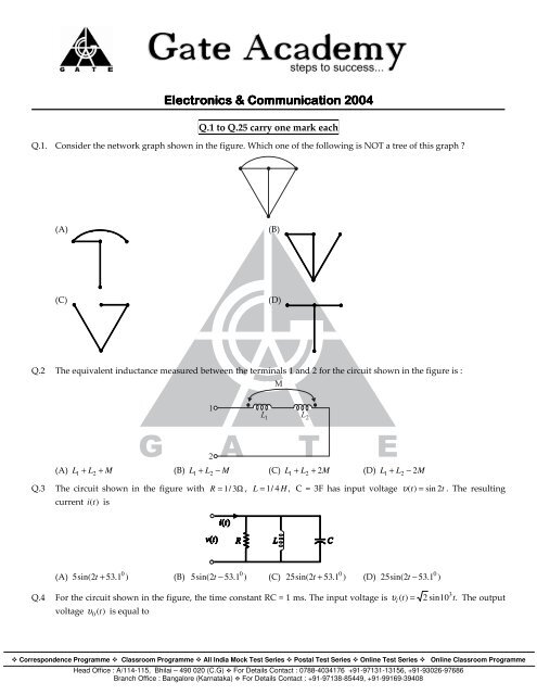
Q.1. Consider the network graph shown in the figure. Which one of the following is NOT a tree of this graph <br />
(A)<br />
(B)<br />
(C)<br />
(D)<br />
Q.2 The equivalent inductance measured between the terminals 1 and 2 for the circuit shown in the figure is :<br />
(A)<br />
L 1 + L 2 + M<br />
(B) L 1 + L 2 − M (C) L1 + L2<br />
+ 2M<br />
(D) L1 + L2<br />
− 2M<br />
Q.3 The circuit shown in the figure with R = 1/ 3Ω<br />
, L = 1/<br />
4 H,<br />
C = 3F has input voltage υ ( t)<br />
= sin 2t<br />
. The resulting<br />
current i (t)<br />
is<br />
0<br />
0<br />
(A) 5sin(2t + 53.1 )<br />
(B) 5sin(2t − 53.1 ) (C) 25sin(2t + 53.1 ) (D) 25sin(2t<br />
− 53.1 )<br />
Q.4 For the circuit shown in the figure, the time constant RC = 1 ms. The input voltage is υ ( t)<br />
2 sin10 . The output<br />
voltage υ ( ) is equal to<br />
0 t<br />
0<br />
i =<br />
0<br />
3 t<br />
Correspondence Programme Classroom Programme All India Mock Test Series Postal Test Series Online Test Series Online Classroom Programme<br />
Head Office : A/114-115, Bhilai – 490 020 (C.G) For Details Contact : 0788-4034176 +91-97131-13156, +91-93026-97686<br />
Branch Office : Bangalore (Karnataka) For Details Contact : +91-97138-85449, +91-99169-39408
EC – <strong>2004</strong> www.gateacademy.co.in<br />
3 −<br />
0<br />
3 +<br />
0<br />
(A) sin(10 t 45 )<br />
(B) sin(10 t 45 ) (C) sin(10 t 53 ) (D) sin(10 t 53 )<br />
Q.5 For the R-L circuit shown in the figure, the input voltage υ ( t)<br />
u(<br />
t)<br />
. The current i (t)<br />
is<br />
i =<br />
3 −<br />
0<br />
3 +<br />
0<br />
(A)<br />
(B)<br />
(C)<br />
(D)<br />
Q.6 The impurity commonly used for realizing the base region of a silicon n-p-n transistor is<br />
(A) Gallium (B) Indium (C) Boron (D) Phosphorus<br />
Q.7 If for a silicon n-p-n transistor, the base-to-emitter voltage ( V EE ) is 0.7V and the collector-to-base voltage ( V CE ) is<br />
0.2V, then the transistor is operating in the<br />
(A) normal active mode (B) saturation mode (C) inverse active mode (D) cutoff mode<br />
Q.8 Consider the following statements S1 and S2.<br />
S1 : The β of a bipolar transistor reduces if the base width is increased.<br />
S2: The β of a bipolar transistor increases if the doping concentration in the base is increased.<br />
Which one of the following is correct<br />
(A) S1 is FALSE and S2 is TRUE<br />
(C) Both S1 and S2 are FALSE<br />
Q.9 An ideal op-amp is an ideal<br />
(A) Voltage controlled current source<br />
(C) Current controlled current source<br />
Q.10 Voltage series feedback (also called series-shunt feedback) results in<br />
(A) increase in both input and output impedances<br />
(B) decrease in both input and output impedances<br />
(C) increase in input impedance and decrease in output impedance<br />
(B) Both S1 and S2 are TRUE<br />
(D) S1 is TRUE and S2 is FALSE<br />
(B) Voltage controlled voltage source<br />
(D) Current controlled voltage source<br />
Correspondence Programme Classroom Programme All India Mock Test Series Postal Test Series Online Test Series Online Classroom Programme<br />
Head Office : A/114-115, Bhilai – 490 020 (C.G) For Details Contact : 0788-4034176 +91-97131-13156, +91-93026-97686<br />
Branch Office : Bangalore (Karnataka) For Details Contact : +91-97138-85449, +91-99169-39408
EC – <strong>2004</strong> www.gateacademy.co.in<br />
(D) decrease in input impedance and increase in output impedance<br />
Q.11 The circuit in the given figure is a<br />
(A) Low-pass filter (B) High-pass filter (C) Band-pass filter (D) Band-reject filter<br />
Q.12 Assuming V CEsat = 0. 2V<br />
and β = 50,<br />
the minimum base current I ) required to drive the transistor in the given<br />
figure to saturation is<br />
( B<br />
(A)<br />
56 µ A<br />
(B) 140mA (C) 60 µ A<br />
(D) 3 mA<br />
Q.13 A master-slave flip-flop has the characteristic that<br />
(A) Change in the input is immediately reflected in the output<br />
(B) Change in the output occurs when the state of the master is affected<br />
(C) Change in the output occurs when the state of the slave is affected.<br />
(D) Both the master and the slave states are affected at the same time<br />
Q.14 The range of signed decimal numbers that can be represented by 6-bit 1's complement numbers is<br />
(A) -31 to +31 (B) -63 to +64 (C) -64 to +63 (D) -32 to +31<br />
Q.15 A digital system is required to amplify a binary-encoded audio signal. The user should be able to control the gain of<br />
the amplifier from a minimum to a maximum in 100 increments. The minimum number of bits required to encode,<br />
in straight binary, is<br />
(A) 8 (B) 6 (C) 5 (D) 7<br />
Q.16 Choose the correct one from among the alternatives A, B, C, D after matching an item from Group 1 with the most<br />
appropriate item in Group 2.<br />
Group 1 Group 2<br />
P: Shift register 1: Frequency division<br />
Q: Counter 2: Addressing in memory chips<br />
R: Decoder 3: Serial to parallel data conversion<br />
(A) P-3, Q-2, R-1 (B) P – 3, Q – 1, R – 2<br />
(C) P – 2, Q – 1, R – 3 (D) P – 1, Q – 2, R – 2<br />
Q.17 Figure given below shows the internal schematic of TTL AND-Or-Invert (AOI) gate. For the inputs shown in the<br />
figure, the output Y is<br />
Correspondence Programme Classroom Programme All India Mock Test Series Postal Test Series Online Test Series Online Classroom Programme<br />
Head Office : A/114-115, Bhilai – 490 020 (C.G) For Details Contact : 0788-4034176 +91-97131-13156, +91-93026-97686<br />
Branch Office : Bangalore (Karnataka) For Details Contact : +91-97138-85449, +91-99169-39408
EC – <strong>2004</strong> www.gateacademy.co.in<br />
(A) 0 (B) 1 (C) AB (D) AB<br />
Q.18 Given Figure is the voltage transfer characteristic of<br />
(A) an NMOS inverter with enhancement mode transistor as load<br />
(B) An NMOS inverter with depletion mode transistor as load<br />
(C) A CMOS inverter<br />
(D) A BJT inverter<br />
Q.19 The impulse response h(n) of a linear time-invariant system is given by<br />
h [ n]<br />
= u[<br />
n + 3] + u[<br />
n − 2] − 2u[<br />
n − 7]<br />
When u [n]<br />
is the unit step sequence. The above system is<br />
(A) Stable but not causal (B) Stable and causal<br />
(C) Causal but unstable<br />
(D) unstable and not causal<br />
Q.20 The distribution function F x (x)<br />
of a random variable X is shown in the figure. The probability that X = 1 is<br />
(A) Zero (B) 0.25 (C) 0.55 (D) 0.30<br />
Q.21 The z-transform of a system is<br />
z<br />
H ( z)<br />
= z − 0.2<br />
If the ROC is | z | < 0.2,<br />
then the impulse response of the system is<br />
n<br />
(A) ( 0.2) u[<br />
n]<br />
(B) ( 0.2) u[<br />
−n −1]<br />
n<br />
n<br />
(C) − ( 0.2) u[<br />
n]<br />
(D) − ( 0.2) u[<br />
−n<br />
−1]<br />
n<br />
Q.22 The fourier transform of a conjugate symmetric function is always.<br />
(A) imaginary<br />
(C) Real<br />
(B) conjugate anti-symmetric<br />
(D) Conjugate symmetric<br />
Q.23 The gain margin for the system with open-loop transfer function<br />
Correspondence Programme Classroom Programme All India Mock Test Series Postal Test Series Online Test Series Online Classroom Programme<br />
Head Office : A/114-115, Bhilai – 490 020 (C.G) For Details Contact : 0788-4034176 +91-97131-13156, +91-93026-97686<br />
Branch Office : Bangalore (Karnataka) For Details Contact : +91-97138-85449, +91-99169-39408
EC – <strong>2004</strong> www.gateacademy.co.in<br />
Q.24 Given<br />
2(1 + s)<br />
G(<br />
s)<br />
H ( s)<br />
= , is<br />
2<br />
s<br />
(A) ∞ (B) 0 (C) 1 (D) −∞<br />
K<br />
G ( s)<br />
H ( s)<br />
=<br />
s(<br />
s + 1)( s + 3)<br />
The point of intersection of the asymptotes of the root loci with the real axis is<br />
(A) - 4 (B) 1.33 (C) -1.33 (D) 4<br />
Q.25 In a PCM system, if the code word length is increased from 6 to 8 bits, the signal to quantization noise ratio<br />
improves by the factor<br />
(A) 8/6 (B) 12 (C) 16 (D) 8<br />
Q.26 An AM signal is detected using an envelope detector. The carrier frequency and modulating signal frequency are 1<br />
MHz and 2 kHz respectively. An appropriate value for the time constant of the envelope detector is<br />
(A)<br />
500µ sec<br />
(B) 20µ sec<br />
(C) 0 .2µ sec<br />
(D) 1µ sec<br />
Q.27 An AM signal and a narrow-band FM signal with identical carriers, modulating signals and modulation indices of<br />
0.1 are added together. The resultant signal can be closely approximated by<br />
(A) Broadband FM (B) SSB with carrier (C) DSB-SC (D) SSB without carrier<br />
Q.28 In the output of a DM speech encoder, the consecutive pulses are of opposite polarity during time interval t1 ≤ t ≤ t2<br />
. This indicates that during this interval<br />
(A) the input to the modulator is essentially constant<br />
(B) the modulator is going through slope overload<br />
(C) the accumulator is in saturation<br />
(D) the speech signal is being sampled at the Nyquist rate<br />
Q.29 The phase velocity of an electromagnetic wave propagating in a hollow metallic rectangular waveguide in the TE 10<br />
mode is<br />
(A) equal to its group velocity<br />
(B) less than the velocity of light in free space<br />
(C) equal to the velocity of light in free space<br />
(D) Greater than the velocity of light in free space<br />
Q.30 Consider a lossless antenna with a directive gain of +6 dB. If 1mW of power is fed to it the total power radiated by<br />
the antenna will be<br />
(A) 4 mW (B) 1 mW (C) 7 mW (D) 1/4 mW<br />
Q.31 to Q.90 carry two marks each<br />
Q.31 For the lattice circuit shown in the figure, Z = 2Ω<br />
and Z = 2Ω<br />
. The values of the open circuit impedance<br />
⎡Z<br />
⎤<br />
parameters =<br />
11 Z<br />
Z<br />
12<br />
⎢<br />
⎣<br />
⎥<br />
are<br />
Z21<br />
Z22<br />
⎦<br />
0 j<br />
b<br />
Correspondence Programme Classroom Programme All India Mock Test Series Postal Test Series Online Test Series Online Classroom Programme<br />
Head Office : A/114-115, Bhilai – 490 020 (C.G) For Details Contact : 0788-4034176 +91-97131-13156, +91-93026-97686<br />
Branch Office : Bangalore (Karnataka) For Details Contact : +91-97138-85449, +91-99169-39408
EC – <strong>2004</strong> www.gateacademy.co.in<br />
(A)<br />
⎡1<br />
− j<br />
⎢⎣ 1+<br />
j<br />
1+<br />
j⎤<br />
1+<br />
j⎥⎦<br />
(B)<br />
⎡ 1−<br />
j<br />
⎢⎣ −1+<br />
j<br />
1+<br />
j⎤<br />
1−<br />
j⎥⎦<br />
(C)<br />
⎡1<br />
+ j<br />
⎢⎣ 1−<br />
j<br />
1+<br />
j⎤<br />
1−<br />
j⎥⎦<br />
(D)<br />
⎡ 1−<br />
j<br />
⎢⎣ −1−<br />
j<br />
−1+<br />
j⎤<br />
1−<br />
j ⎥⎦<br />
Q.32 The circuit shown in the figure has initial current i L ( 0 ) = 1A<br />
−<br />
−<br />
through the inductor and an initial voltage<br />
υ C ( 0 ) = −1V<br />
across the capacitor. For input υ ( t ) = u(<br />
t)<br />
, the Laplace transform of the current i (t)<br />
for t > 0 is<br />
(A)<br />
s<br />
2<br />
s<br />
(B)<br />
+ s + 1<br />
s<br />
s + 2<br />
2<br />
+ s + 1<br />
(C)<br />
s<br />
2<br />
s −1<br />
+ s + 1<br />
(D)<br />
s<br />
s − 2<br />
2<br />
+ s + 1<br />
Q.33 Consider the Bode magnitude plot shown in the given figure. The transfer function H(s) is<br />
(A)<br />
( s + 10)<br />
( s + 1) ( s + 100)<br />
(B)<br />
10( s + 1)<br />
( s + 10) ( s + 100)<br />
(C)<br />
( 1)<br />
( +10 2 s +<br />
s 10) ( s + 100)<br />
(D)<br />
10 3 ( s + 100)<br />
( s + 1) ( s + 10)<br />
Q.34 The transfer function<br />
V0<br />
( s)<br />
H ( s)<br />
= of an R-L-C circuit is given by<br />
V ( s)<br />
i<br />
H ( s)<br />
=<br />
s<br />
2<br />
10<br />
6<br />
+ 20s<br />
+ 10<br />
The Quality factor (Q-factor) of this circuit is<br />
(A) 25 (B) 50 (C) 100 (D) 5000<br />
Q.35 For the circuit shown in the figure,the initial conditions are zero. Its transfer function H ( s)<br />
= V ( s) / V ( s)<br />
is<br />
6<br />
C<br />
i<br />
Correspondence Programme Classroom Programme All India Mock Test Series Postal Test Series Online Test Series Online Classroom Programme<br />
Head Office : A/114-115, Bhilai – 490 020 (C.G) For Details Contact : 0788-4034176 +91-97131-13156, +91-93026-97686<br />
Branch Office : Bangalore (Karnataka) For Details Contact : +91-97138-85449, +91-99169-39408
EC – <strong>2004</strong> www.gateacademy.co.in<br />
(A)<br />
s<br />
2<br />
1<br />
3<br />
+ 10 s + 10<br />
6<br />
(B)<br />
s<br />
2<br />
10<br />
3<br />
6<br />
+ 10 s + 10<br />
6<br />
(C)<br />
s<br />
2<br />
10<br />
3<br />
3<br />
+ 10 s + 10<br />
6<br />
(D)<br />
s<br />
2<br />
10<br />
6<br />
6<br />
+ 10 s + 10<br />
6<br />
Q.36 A system described by the following differential equation<br />
2<br />
d y dy<br />
+ 3 + 2y<br />
= x(<br />
t)<br />
2<br />
dt dt<br />
is initially at rest. For input x ( t)<br />
= 2u(<br />
t),<br />
the output y(t) is<br />
− t<br />
+<br />
−2t<br />
(A) (1 − 2e<br />
e ) u(<br />
t)<br />
(B) (1 + 2e<br />
− e ) u(<br />
t)<br />
− t<br />
+<br />
−2t<br />
(C) (0.5 + e 1.5e<br />
) u(<br />
t)<br />
(D) (0.5 + 2e<br />
2e<br />
) u(<br />
t)<br />
Q.37 Consider the following statements S1 and S2.<br />
S1 : At the resonant frequency the impedance of a series R-L-C circuit is zero.<br />
S2: In a parallel G-L-C circuit, increasing the conductance G results in increase in its Q factor.<br />
Which one of the following is correct <br />
− t<br />
− t<br />
+<br />
−2t<br />
−2t<br />
(A) S1 is FALSE and S2 is TRUE<br />
(C) S1 is TRUE and S2 is FALSE<br />
(B) Both S1 and S2 are TRUE<br />
(D) Both S1 and S2 are FALSE<br />
Q.38 In an abrupt p-n junction, doping concentrations on the p-side and n-side are<br />
N<br />
A<br />
= 9× 10 /cm and N = 1×<br />
10 /cm<br />
16 3 16 3<br />
D<br />
respectively. The p-n junction is reverse biased and the total depletion width is 3µ m.<br />
The depletion width on the p-<br />
side is<br />
(A)<br />
2 .7µ m<br />
(B) 0 .3µ m<br />
(C) 2 .25µ m (D) 0 .75µ m<br />
Q.39 The resistivity of a uniformly doped n-type silicon sampled is 0.5Ω − cm.<br />
If the electron mobility µ ) is 1250<br />
2<br />
cm / V − sec and the charge of an electron is<br />
sample is<br />
−19<br />
1.6× 10 coulomb, the donor impurity concentration N ) in the<br />
( n<br />
( D<br />
(A)<br />
3<br />
2× 10 16 / cm<br />
(B)<br />
3<br />
1× 10 16 / cm (C)<br />
2.5× 10 15 / cm (D)<br />
3<br />
5×<br />
10 15 / cm<br />
3<br />
Q.40 Consider an abrupt p-n junction. Let V bi be the built-in potential of this junction and V π be the applied reverse bias.<br />
If the junction capacitance ( C ) is 1 pF for V V = 1V,<br />
then for V = 4V,<br />
C will be<br />
j<br />
bi + R<br />
V bi + R<br />
j<br />
(A) 4 pF (B) 2 pF (C) 0.25 pF (D) 0.5 pF<br />
Q.41 Consider the following statements S1 and S2.<br />
S1: the threshold voltage ( V T ) of a MOS capacitor decreases with increase in gate oxide thickness.<br />
S2: the threshold voltage ( V T ) of a MOS capacitor decreases with increase in substrate doping concentration.<br />
Which one of the following is correct<br />
(A) S1 is FALSE and S2 is TRUE<br />
(B) Both S1 and S2 are TRUE<br />
Correspondence Programme Classroom Programme All India Mock Test Series Postal Test Series Online Test Series Online Classroom Programme<br />
Head Office : A/114-115, Bhilai – 490 020 (C.G) For Details Contact : 0788-4034176 +91-97131-13156, +91-93026-97686<br />
Branch Office : Bangalore (Karnataka) For Details Contact : +91-97138-85449, +91-99169-39408
EC – <strong>2004</strong> www.gateacademy.co.in<br />
(C) Both S1 and S2 are FALSE<br />
(D) S1 is TRUE and S2 is FALSE<br />
Q.42 The drain of an n-channel MOSFET is shorted to the gate so that V GS = VDS<br />
. The threshold voltage ( V T ) of MOSFET<br />
is 1 V. If the drain current ( I D ) is 1mA for V GS = 2V , then for V GS = 3V , I D is<br />
(A) 2 mA (B) 3 mA (C) 9 mA (D) 4 m<br />
Q.43 The longest wavelength that can be absorbed by silicon, which has the bandgap of 1.12 eV, is 1.1µ m. If the longest<br />
wavelength that can be absorted by another material is 0.87µ m , then the bandgap of this material is<br />
(A) 1.416 eV (B) 0.886 eV (C) 0.854 eV (D) 0.706 eV<br />
Q.44 The neutral base width of a bipolar transistor, biased in the active region, is 0.5µ m.<br />
The maximum electron<br />
concentration and the diffusion constant in the base are<br />
14 3<br />
10 /cm and<br />
2<br />
D<br />
n<br />
= 25 cm /sec respectively. Assuming<br />
−19<br />
negligible recombination in the base, the collector current density is (the electron charge is 1.6× 10 Coulomb)<br />
(A)<br />
2<br />
800 A/cm (B)<br />
2<br />
8 A/cm (C)<br />
2<br />
200 A/cm (D)<br />
2 A/cm<br />
2<br />
Q.45 Assume that the β of the transistor is extremely large and V BE = 0.7V<br />
, I C and V CE in the circuit shown in the figure<br />
are<br />
(A)<br />
(C)<br />
I 1 mA,<br />
V = 4.7 V<br />
(B) I 0 .5mA,<br />
V = 3.75V<br />
C = CE<br />
C = CE<br />
I 1 mA,<br />
V = 2.5V<br />
(D) I 0 .5mA,<br />
V = 3.9V<br />
C = CE<br />
C = CE<br />
Q.46 A bipolar transistor is operating in the active region with a collector current of 1 mA. Assuming that the β of the<br />
transistor is 100 and the thermal voltage ( V T ) is 25mV, the Tranconductance ( g m ) and the input resistance r ) of<br />
the transistor in the common emitter configuration, are<br />
(A) g = 25 mA/V and = 15.625 kΩ (B) g = 40 mA/V and = 4.0 kΩ<br />
m<br />
r π<br />
(C) g = 25 mA/V and = 2.5 kΩ (D) g = 40 mA/V and = 2.5 kΩ<br />
m<br />
r π<br />
Q.47 The value of C required for sinusoidal oscillations of frequency 1 KHz in the circuit of given figure is :<br />
m<br />
m<br />
r π<br />
r π<br />
( π<br />
Correspondence Programme Classroom Programme All India Mock Test Series Postal Test Series Online Test Series Online Classroom Programme<br />
Head Office : A/114-115, Bhilai – 490 020 (C.G) For Details Contact : 0788-4034176 +91-97131-13156, +91-93026-97686<br />
Branch Office : Bangalore (Karnataka) For Details Contact : +91-97138-85449, +91-99169-39408
EC – <strong>2004</strong> www.gateacademy.co.in<br />
(A)<br />
1<br />
µ F<br />
2π<br />
(B)<br />
1<br />
2 πµ F<br />
(C) µ F<br />
2π 6<br />
Q.48 In the op-amp circuit given in the figure, the load current i L is<br />
(D)<br />
2 π 6µ F<br />
(A)<br />
υ<br />
− s<br />
(B)<br />
R 2<br />
υ s<br />
R 2<br />
(C)<br />
υs<br />
− (D)<br />
R<br />
L<br />
υ s<br />
R 1<br />
Q.49 In the voltage regulator shown in the given figure, the load current can vary from 100 mA to 500 mA. Assuming<br />
that a Zener diode is ideal (i.e. the Zener knee current is negligibly small and Zener resistance is zero in the<br />
breakdown region), the value of R is<br />
(A)<br />
7 Ω<br />
(B) 70 Ω<br />
(C) 70 / 3Ω<br />
(D) 14 Ω<br />
Q.50 In a full–wave rectifier using two ideal diodes, Vdc<br />
andV m are the dc and peak values of the voltage respectively<br />
across a resistive load. If PIV is the peak inverse voltage of the diode, then the appropriate relationships for this<br />
rectifier are<br />
Vm<br />
Vm<br />
(A) Vdc<br />
= , PIV = 2V<br />
π<br />
m<br />
(B) I dc = 2 , PIV = 2Vm<br />
π<br />
(C)<br />
V<br />
V = , =<br />
dc<br />
m<br />
m<br />
2 PIV V<br />
π<br />
m<br />
(D) V dc = , PIV = Vm<br />
Q.51 The minimum number of 2-to-1 multiplexers required to realize a 4-to-1 multiplexer is<br />
(A) 1 (B) 2 (C) 3 (D) 4<br />
Q.52 The Boolean expression AC + BC is equivalent to<br />
V<br />
π<br />
Correspondence Programme Classroom Programme All India Mock Test Series Postal Test Series Online Test Series Online Classroom Programme<br />
Head Office : A/114-115, Bhilai – 490 020 (C.G) For Details Contact : 0788-4034176 +91-97131-13156, +91-93026-97686<br />
Branch Office : Bangalore (Karnataka) For Details Contact : +91-97138-85449, +91-99169-39408
EC – <strong>2004</strong> www.gateacademy.co.in<br />
(A)<br />
(C)<br />
A C + BC + AC<br />
(B) B C + AC + BC + ACB<br />
AC + BC + BC + ABC<br />
(D) ABC + ABC + ABC + ABC<br />
Q.53 11001, 1001 and 111001 correspond to the 2's complement representation of which one of the following sets of<br />
numbers<br />
(A) 25, 9 and 57 respectively<br />
(C) -7, -7 and -7 respectively<br />
(B) -6, -6 and -6 respectively<br />
(D) -25, -9 and -57 respectively<br />
Q.54 The 8255 programmable peripheral Interface is used as described below.<br />
(i) An A/D converter is interfaced to a microprocessor through an 8255. The conversion is initiated by a signal<br />
from the 8255 on Port C. A signal on Port C causes data to be stobed into Port A.<br />
(ii) Two computers exchange data using a pair of 8255s. Port A works as a bidirectional data port supported by<br />
appropriate handshaking signals.<br />
The appropriate modes of operation of the 8255 for (i) and (ii) would be<br />
(A) Mode 0 for (i) and Mode 1 for (ii)<br />
(C) Mode 2 for (i) and Mode 0 for (ii)<br />
(B) Mode 1 for (i) and Mode 2 for (ii)<br />
(D) Mode 2 for (i) and Mode 1 for (ii)<br />
Q.55 The number of memory cycles required to execute the following 8085 instructions<br />
(i) LDA 3000H<br />
(ii) LXI D, FOF1H<br />
Would be<br />
(A) 2 for (i) and 2 for (ii)<br />
(C) 3 for (i) and 3 for (ii)<br />
(B) 4 for (i) and 2 for (ii)<br />
(D) 3 for (i) and 4 for (ii)<br />
Q.56 In the modulo-6 ripple counter shown in the given figure, the output of the 2-input gate is used to clear the J-K flipflops.<br />
The 2-input gate is<br />
(A) A NAND gate (B) A NOR gate (C) an OR gate (D) an AND gate<br />
Q.57 Consider the sequence of 8085 instructions given below<br />
LXI H, 9258<br />
MOV A, M<br />
CMA<br />
MOV M, A<br />
Which one of the following is performed by this sequence<br />
(A) Contents of location 9258 are moved to the accumulator<br />
Correspondence Programme Classroom Programme All India Mock Test Series Postal Test Series Online Test Series Online Classroom Programme<br />
Head Office : A/114-115, Bhilai – 490 020 (C.G) For Details Contact : 0788-4034176 +91-97131-13156, +91-93026-97686<br />
Branch Office : Bangalore (Karnataka) For Details Contact : +91-97138-85449, +91-99169-39408
(B) Contents of location 9258 are compared with the contents of the accumulator<br />
(C) Contents of location 8529 are complemented and stored in location 8529<br />
(D) Contents of location 5892 are complemented and stored in location 5892<br />
Q.58 A Boolean function f of two variables x and y is defined as follows :<br />
f ( 0, 0) = f (0, 1) = f (1, 1) = 1; f (1, 0) = 0<br />
EC – <strong>2004</strong> www.gateacademy.co.in<br />
Assuming complements of x and y are not available, a minimum cost solution for realizing f using only 2-input<br />
NOR gates and 2-input OR gates (each having unit cost) would have a total cost of<br />
(A) 1 unit (B) 4 units (C) 3 units (D) 2 units<br />
Q.59 It is desired to multiply the numbers 0AH by 0BH and store the result in the accumulator. The numbers are<br />
available in registers B and C respectively. A part of the 8085 program for this purpose is given below :<br />
MVI A, 00H<br />
LOOP :<br />
_ _ _ _ _ _ _ _ _<br />
_ _ _ _ _ _ _ _ _<br />
_ _ _ _ _ _ _ _ _<br />
HLT<br />
END<br />
The sequence of instruction to complete the program would be<br />
(A) JNZ LOOP, ADD B, DCR C<br />
(C) DCR C, JNZ LOOP, ADD B<br />
(B) ADD B, JNZ LOOP, DCR C<br />
(D) ADD B, DCR C, JNZ LOOP<br />
Q.60 A 1 KHz sinusoidal signal is ideally sampled at 1500 samples/sec and the sampled signal is passed through an ideal<br />
low-pass filter with cut-off frequency 800 Hz. The output signal has the frequency<br />
(A) zero Hz (B) 0.75 KHz (C) 0.5 KHz (D) 0.25 KHz<br />
Q.61 A rectangular pulse train s(t) as shown in the figure is convolved with the signal cos (4π × 10 t).<br />
The convolved<br />
signal will be a<br />
2<br />
3<br />
(A) DC (B) 12 KHz Sinusoid (C) 8 KHz sinusoid (D) 14 KHz sinusoid<br />
Q.62 Consider the sequence<br />
x[ n]<br />
= [ −4<br />
− j5<br />
1+<br />
j2<br />
5]<br />
↑<br />
The conjugate anti-symmetric part of the sequence is<br />
(A) [-4 – j25 j2 4 – j25]<br />
(B) [-j25 1 j2.5]<br />
Correspondence Programme Classroom Programme All India Mock Test Series Postal Test Series Online Test Series Online Classroom Programme<br />
Head Office : A/114-115, Bhilai – 490 020 (C.G) For Details Contact : 0788-4034176 +91-97131-13156, +91-93026-97686<br />
Branch Office : Bangalore (Karnataka) For Details Contact : +91-97138-85449, +91-99169-39408
EC – <strong>2004</strong> www.gateacademy.co.in<br />
(C) [-j2.5 j2 0] (D) -4, 1 4]<br />
Q.63 A causal LTI system is described by the difference equation<br />
2y[<br />
n]<br />
= α y[<br />
n − 2] − 2x[<br />
n]<br />
+ βx[<br />
n −1]<br />
The system is stable only if<br />
(A) | α | = 2, | β | < 2<br />
(B) | α | > 2, | β | > 2<br />
(C)<br />
| α | < 2, any value of β<br />
(D) | β | < 2, any value of α<br />
Q.64 A causal system having the transfer function<br />
1<br />
H ( s)<br />
= s + 2<br />
is excited with 10u<br />
( t)<br />
. The time at which the output reaches 99% of its steady state value is<br />
(A) 2.7 sec (B) 2.5 sec (C) 2.3 sec (D) 2.1 sec<br />
Q.65 The impulse response h [n]<br />
of a linear time invariant system is given as<br />
⎧−<br />
2 2 n = 1, −1<br />
⎪<br />
h [ n]<br />
= ⎨4<br />
2 n = 2, − 2<br />
⎪ 0 otherwise<br />
⎩<br />
j n/ 4<br />
e π<br />
If the input to the above system is the sequence ,<br />
then the output is<br />
(A)<br />
4<br />
2<br />
j n/<br />
4<br />
e π<br />
(B)<br />
4<br />
2e<br />
− j π n / 4<br />
(C)<br />
4<br />
j n/<br />
4<br />
e π<br />
(D)<br />
− 4<br />
j n / 4<br />
e π<br />
Q.66 Let x (t)<br />
and y (t)<br />
with Fourier transforms X(f) and Y(f) respectively be related as shown in the given figure. Then<br />
Y ( f ) is<br />
(A)<br />
1 − j2πf<br />
− X ( f / 2) e<br />
(B)<br />
2<br />
1<br />
j2πf<br />
− X ( f / 2) e (C)<br />
2<br />
j2πf<br />
− X ( f / 2) e (D)<br />
− X ( f / 2) e<br />
− j2πf<br />
Q.67 A system has poles at 0.01 Hz, 1 Hz and 80 Hz; zeros at 5 Hz, 100 Hz and 200 Hz. The approximate phase of the<br />
system response at 20 Hz is<br />
(A)<br />
0<br />
− 90<br />
(B)<br />
0<br />
0 (C)<br />
0<br />
90 (D)<br />
0<br />
− 180<br />
Q.68 Consider the signal flow graph shown in the figure below. The gain<br />
x<br />
x<br />
5<br />
1<br />
is<br />
Correspondence Programme Classroom Programme All India Mock Test Series Postal Test Series Online Test Series Online Classroom Programme<br />
Head Office : A/114-115, Bhilai – 490 020 (C.G) For Details Contact : 0788-4034176 +91-97131-13156, +91-93026-97686<br />
Branch Office : Bangalore (Karnataka) For Details Contact : +91-97138-85449, +91-99169-39408
EC – <strong>2004</strong> www.gateacademy.co.in<br />
(A) 1 − ( be + cf + dg)<br />
abc<br />
(B)<br />
bedg<br />
1−<br />
( be + cf + dg)<br />
(C)<br />
abcd<br />
1− ( be + cf + dg)<br />
+ bedg<br />
(D)<br />
1− ( be + cf + dg)<br />
+ bedg<br />
abcd<br />
Q.69 If<br />
A =<br />
⎡−<br />
2<br />
⎢⎣ 1<br />
2 ⎤<br />
, then sin At is<br />
− 3⎥⎦<br />
(A)<br />
1 ⎡sin( − 4 t) + 2sin( −t) −sin( − 4 t) + 2sin( −t)<br />
⎤<br />
3<br />
⎢<br />
−sin( − 4 t) + sin( −t) 2sin( − 4 t) + sin( −t)<br />
⎥<br />
⎣<br />
⎦<br />
(B)<br />
1 ⎡sin( −2 t) sin(2 t)<br />
⎤<br />
3<br />
⎢<br />
sin( t) sin( −3 t)<br />
⎥<br />
⎣<br />
⎦<br />
(C)<br />
1 ⎡sin(4 t) + 2sin( t) 2sin( −4 t) − 2sin( −t)<br />
⎤<br />
3<br />
⎢<br />
−sin( − 4 t) + sin t 2sin(4 t) + sin( t)<br />
⎥<br />
⎣<br />
⎦<br />
(D)<br />
1 ⎡ cos( − t) + 2cos( t) 2cos( −4 t) − 2sin( −t)<br />
⎤<br />
3<br />
⎢<br />
−cos( − 4 t) + sin( −t) − 2cos(4 t) + cos( t)<br />
⎥<br />
⎣<br />
⎦<br />
Q.70 The open-loop transfer function of a unity feedback system is<br />
G ( s)<br />
=<br />
s(<br />
s<br />
2<br />
K<br />
+ s + 2) ( s + 3)<br />
The range of K for which the system is stable is<br />
21<br />
21<br />
(A) > K > 0<br />
(B) 13 > K > 0 (C) < K < ∞<br />
4<br />
4<br />
Q.71 For the polynomial<br />
5<br />
4<br />
P ( s)<br />
= s + s + 2s<br />
+ 2s<br />
+ 3s<br />
+ 15<br />
The number of roots which lie in the right half of the s-plane is<br />
3<br />
2<br />
(D)<br />
−6<br />
< K < ∞<br />
(A) 4 (B) 2 (C) 3 (D) 1<br />
Q.72 The state variable equations of a system are :<br />
ẋ<br />
= −3x − x = u<br />
1.<br />
1 1 2<br />
ẋ<br />
= 2 x ,<br />
2. 2 1<br />
The system is :<br />
y = x + u<br />
1<br />
(A) Controllable but not observable<br />
(C) Neither controllable nor observable<br />
(B) Observable but not controllable<br />
(D) Controllable and observable<br />
Q.73 Given<br />
A =<br />
⎡ 1 ⎤<br />
⎢⎣ 0 1<br />
0 , the state transition matrix<br />
⎥⎦<br />
At<br />
e is given by<br />
(A)<br />
⎡ 0<br />
⎢ −<br />
⎣e<br />
t<br />
−t<br />
e ⎤<br />
0 ⎥ ⎦<br />
(B)<br />
⎡ 0<br />
⎢ t<br />
⎣e<br />
t<br />
e ⎤<br />
0 ⎥ ⎦<br />
(C)<br />
⎡<br />
−<br />
e<br />
⎢<br />
⎣ 0<br />
t<br />
0 ⎤<br />
−t<br />
e ⎥ ⎦<br />
(D)<br />
⎡<br />
t<br />
e<br />
⎢<br />
⎣ 0<br />
0 ⎤<br />
t<br />
e ⎥ ⎦<br />
Correspondence Programme Classroom Programme All India Mock Test Series Postal Test Series Online Test Series Online Classroom Programme<br />
Head Office : A/114-115, Bhilai – 490 020 (C.G) For Details Contact : 0788-4034176 +91-97131-13156, +91-93026-97686<br />
Branch Office : Bangalore (Karnataka) For Details Contact : +91-97138-85449, +91-99169-39408
EC – <strong>2004</strong> www.gateacademy.co.in<br />
Q.74 Consider the signal x(t) shown in the figure. Let h(t) denote the impulse response of the filter matched to x (t)<br />
, with<br />
h (t) being non-zero only in the interval 0 to 4 sec. The slope of h (t)<br />
in the inverval 3 < t < 4 sec is<br />
(A)<br />
1 −1<br />
sec<br />
2<br />
(B)<br />
−1<br />
− 1sec<br />
(C)<br />
1 sec<br />
2<br />
−1<br />
− (D)<br />
Q.75 A 1 mW video signal having a bandwidth of 100 MHz is transmitted to a receiver through a cable that has 40 dB<br />
20<br />
loss. IF the effective one-sided noise spectral density at the receiver is 10 − Watt/Hz, then the signal-to-noise ratio<br />
at the receiver is<br />
(A) 50 dB (B) 30 dB (C) 40 dB (D) 60 dB<br />
Q.76 A 100 MHz carrier of 1V amplitude and a 1 MHz modulating signal of 1 V amplitude are fed to a balanced<br />
modulator. The output of the modulator is passed through an ideal high-pass filter with cut-off frequency of 100<br />
0<br />
MHz. The output of the filter is added with 100 MHz signal of 1V amplitude and 90 phase shift as shown in the<br />
given figure. The envelope of the resultant signal is<br />
1sec<br />
−1<br />
6 t<br />
(A) Constant (B) 1+ sin(2π × 10 ) (C) 5 / 4 − sin(2π × 10 ) (D) 5 / 4 + cos(2π<br />
× 10 )<br />
Q.77 Two sinusoidal signals of same amplitude and frequencies 10 KHz and 10.1 KHz are added together. The combined<br />
signal is given to an ideal frequency detector. The output of the detector is<br />
(A) 0.1 KHz sinusoid<br />
(C) a linear function of time<br />
(B) 20.1 KHz sinusoid<br />
(D) a constant<br />
Q.78 Consider a binary digital communication system with equally likely 0's and 1's. When binary 0 is transmitted the<br />
voltage at the detector input can lie between the levels -0.25V and +0.25 V with equal probability; when binary 1 I<br />
transmitted, the voltage at the detector can have any value between 0 and 1 V with equal probability. If the detector<br />
has a threshold of 0.2V (i.e the received signal is greater than 0.2V, the bit is taken as 1), the average bit error<br />
probability is<br />
(A) 0.15 (B) 0.2 (C) 0.05 (D) 0.5<br />
Q.79 A random variable X with uniform density in the interval 0 to 1 is quantized as follows:<br />
if 0 ≤ X ≤ 0.3,<br />
x = 0<br />
if 0 .3 ≤ X ≤ 1, x = 0. 7<br />
q<br />
q<br />
6 t<br />
6 t<br />
Correspondence Programme Classroom Programme All India Mock Test Series Postal Test Series Online Test Series Online Classroom Programme<br />
Head Office : A/114-115, Bhilai – 490 020 (C.G) For Details Contact : 0788-4034176 +91-97131-13156, +91-93026-97686<br />
Branch Office : Bangalore (Karnataka) For Details Contact : +91-97138-85449, +91-99169-39408
EC – <strong>2004</strong> www.gateacademy.co.in<br />
Where x q is the quantized value of X. The root-mean square value of the quantization noise is<br />
(A) 0.573 (B) 0.198 (C) 2.205 (D) 0.266<br />
Q.80 Choose the correct one form among the alternatives A, B, C, D after matching an item from Group 1 with the most<br />
appropriate item in Group 2.<br />
Group 1 Group 2<br />
1 : FM P : Slope overload<br />
2 : DM Q : µ − law<br />
3 : PSK R : Envelope detector<br />
4 : PCM S : Capture effect<br />
T : Hilbert transfer<br />
U : Matched filter<br />
(A) 1-T, 2-P, 3-U, 4-S (B) 1-S, 2-U, 3-P, 4-T<br />
(C) 1-S 2-U, 3-U, 4-Q (D) 1-U, 2-R, 3-S, 4-Q<br />
Q.81 Three analog signals, having bandwidth 1200Hz, 600 Hz and 600 Hz are sampled at their respective Nyquist rates,<br />
encoded with 12 bit words, and time division multiplexed. The bit rate for the multiplexed signal is<br />
(A) 1, 15.2 kbps (B) 28.8 kbps (C) 27.6 kbps (D) 38.4 kbps<br />
Q.82 Consider a system shown in the figure. Let X(f) and Y(f) denote the Fourier transforms of x (t)<br />
and y(t)<br />
The ideal HPF has the cutoff frequency 10 KHz.<br />
respectively.<br />
The positive frequencies where Y(f) has spectral peaks are<br />
(A) 1 KHz and 24 KHz<br />
(C) 1 KHz and 14 KHz<br />
(B) 2 KHz and 24 KHz<br />
(D) 2 KHz and 14 KHz<br />
Q.83 A parallel plate are-filled capacitor has plate area of 10 m<br />
−4<br />
2<br />
and plate separation of<br />
−9<br />
0 m<br />
V, 3.6 GHz source. The magnitude of the displacement current is ( ε = 1/ 36π × 10 F / )<br />
(A) 10 mA (B) 100 mA (C) 10 A (D) 1.59 mA<br />
10 − 3 m . It is connected to a 0.5<br />
Correspondence Programme Classroom Programme All India Mock Test Series Postal Test Series Online Test Series Online Classroom Programme<br />
Head Office : A/114-115, Bhilai – 490 020 (C.G) For Details Contact : 0788-4034176 +91-97131-13156, +91-93026-97686<br />
Branch Office : Bangalore (Karnataka) For Details Contact : +91-97138-85449, +91-99169-39408
EC – <strong>2004</strong> www.gateacademy.co.in<br />
Q.84 A source produces binary data at the rate of 10 kbps. The binary symbols are represented as shown in the figure<br />
given below.<br />
The source output is transmitted using two modulation schemes, namely Binary PSK (BPSK) and Quandrature<br />
PSK(QPSK). Let B 1 and B 2 be the bandwidth requirements of BPSK and QPSK respectively. Assuming that the<br />
bandwidth of the above rectangular pulses is 10 KHz, B 1 and B 2 are<br />
(A) B<br />
1<br />
= 20 KHz , B<br />
2<br />
= 20 KHz<br />
(B) B1 = 10 KHz, B2<br />
= 20 KHz<br />
(C) B1 = 20 KHz, B2<br />
= 10 KHz<br />
(D) B1 = 20 KHz, B2<br />
= 10 KHz<br />
Q.85 Consider a 300 Ω , quanter-wave long (at 1 GHz) transmission line as shown in the figure. It is connected to a 10V,<br />
50 Ω source at one end and is left open circuited at the other end. The magnitude of the voltage at the open circuit<br />
end of the line is<br />
(A) 10 V (B) 5 V (C) 60V (D) 60 / 7 V<br />
Q.86 In a microwave test bench, why is the microwave signal amplitude modulated at 1 KHz<br />
(A) To increase the sensitivity of measurement<br />
(B) to transmit the signal to a far-off place<br />
(C) to study amplitude modulation<br />
(D) Because crystal detector fails at microwave frequencies<br />
<br />
<br />
jkz−<br />
jωt<br />
jkz−<br />
jωt<br />
Q.87 If E = ( aˆ<br />
+ jaˆ<br />
) e and H = ( k / ωµ )( aˆ<br />
+ jaˆ<br />
) e , the time-averaged Poynting vector is<br />
x<br />
y<br />
(A) Null vector (B) ( k / ωµ )<br />
(C) ( 2k<br />
/ ωµ ) â (D) ( k / 2ωµ<br />
)<br />
z<br />
y<br />
x<br />
Q.88 Consider an impedance Z = R + jX marked with point P in an impedance Smith chart as shown in the figure. The<br />
0<br />
movement from point P along a constant resistance circle in the clockwise direction by an angle 45 is equivalent to<br />
â z<br />
â z<br />
Correspondence Programme Classroom Programme All India Mock Test Series Postal Test Series Online Test Series Online Classroom Programme<br />
Head Office : A/114-115, Bhilai – 490 020 (C.G) For Details Contact : 0788-4034176 +91-97131-13156, +91-93026-97686<br />
Branch Office : Bangalore (Karnataka) For Details Contact : +91-97138-85449, +91-99169-39408
EC – <strong>2004</strong> www.gateacademy.co.in<br />
(A) adding an inductance is series with Z<br />
(B) adding a capacitance in series with Z<br />
(C) adding an inductance in shunt across Z<br />
(D) adding a capacitance in shunt across Z<br />
Q.89 A plane electromagnetic wave propagating in free space in incident normally on a large slab of loss-less, nonmagnetic,dielectric<br />
material with ε > ε 0 . Maxima and minima are observed when the electric field is measured in<br />
front of the slab. The maximum electric field is found to be 5 times the minimum field. The instrinsic impedance of<br />
the medium should be<br />
(A)<br />
120 πΩ<br />
(B) 60 πΩ<br />
(C) 600 πΩ<br />
(D) 24 πΩ<br />
Q.90 A lossless transmission line is terminated in a load which reflects a part of the incident power. The measured VSWR<br />
is 2. The percentage of the power that is reflected back is<br />
(A) 57.73 (B) 33.33 (C) 0.11 (D) 11.11<br />
END OF THE QUESTION PAPER<br />
Correspondence Programme Classroom Programme All India Mock Test Series Postal Test Series Online Test Series Online Classroom Programme<br />
Head Office : A/114-115, Bhilai – 490 020 (C.G) For Details Contact : 0788-4034176 +91-97131-13156, +91-93026-97686<br />
Branch Office : Bangalore (Karnataka) For Details Contact : +91-97138-85449, +91-99169-39408