tbp testengineering - Hardware Conference
tbp testengineering - Hardware Conference
tbp testengineering - Hardware Conference
- No tags were found...

You also want an ePaper? Increase the reach of your titles
YUMPU automatically turns print PDFs into web optimized ePapers that Google loves.
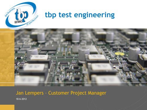
<strong>tbp</strong> test engineering<br />
Jan Lempers – Customer Project Manager<br />
18-6-2012
product creation<br />
Review<br />
Customer<br />
needs<br />
Design<br />
input<br />
Design<br />
process<br />
Design<br />
output<br />
Engineering<br />
sample<br />
Prototype<br />
Product<br />
Verification<br />
Pre-Qualification<br />
Qulaification<br />
2<br />
©<strong>tbp</strong> electronics bv
design for eXcellence (DfX)<br />
3<br />
©<strong>tbp</strong> electronics bv
design for test<br />
The aspects of the product design process whose goal is<br />
to ensure that the testability of the end product is<br />
competently and sufficiently developed.<br />
4<br />
©<strong>tbp</strong> electronics bv
the ideal world<br />
Pass<br />
First-Pass<br />
Yield<br />
100%<br />
Good<br />
Faulty<br />
Known Good<br />
Boards:<br />
100%<br />
Slip: 0%<br />
Production<br />
Yield<br />
100%<br />
Test<br />
Efficiency<br />
100%<br />
5 ©<strong>tbp</strong> electronics bv
est-in-class reality<br />
no structural test,<br />
only AOI.<br />
Pass<br />
First-Pass<br />
Yield<br />
93,77%<br />
Good<br />
Faulty<br />
Known Good<br />
Boards:<br />
92,12%<br />
Slip: 1,65%<br />
Production<br />
Yield<br />
92,59%<br />
Testway<br />
Test<br />
Efficiency<br />
77,75%<br />
Fall-Off<br />
Rate:<br />
6,22%<br />
False<br />
Rejects:<br />
0,46%<br />
Known Bad<br />
Boards:<br />
5,76%<br />
6 ©<strong>tbp</strong> electronics bv
test strategy<br />
how to get the proper test strategy<br />
early involvement in design process<br />
dialogue with developers during design<br />
implement appropriate test strategy in the design<br />
7<br />
©<strong>tbp</strong> electronics bv
test methods (a)<br />
inspection systems<br />
X-ray<br />
automatic optical inspection (AOI)<br />
structural test systems<br />
boundary scan (BSC)<br />
in-circuit (ICT)<br />
flying probe (FP)<br />
complementary test systems<br />
functional test (FT)<br />
system test<br />
burn-in<br />
8 ©<strong>tbp</strong> electronics bv
x-ray<br />
what can be inspected:<br />
• solder joints (BGA, QFN, …)<br />
• shorts, opens (no cracks)<br />
• discover fake components<br />
pro’s and con’s:<br />
quick program generation ( library )<br />
no tool cost<br />
exact diagnosis: ~ no troubleshoot time<br />
no electrical test<br />
depends on photo-interpretation of operator<br />
development time:<br />
• few minutes/part<br />
9<br />
©<strong>tbp</strong> electronics bv
automatic optical inspection<br />
what can be inspected:<br />
• precense of components<br />
• polarity of components<br />
• optional solder joints<br />
pro’s and con’s:<br />
quick program generation ( library )<br />
no tool cost<br />
exact diagnosis: ~ no troubleshoot time<br />
no electrical test<br />
high false call rate (mainly solder)<br />
development time:<br />
• approximately 2 days (strongly dependent on library)<br />
10<br />
©<strong>tbp</strong> electronics bv
oundary scan (1)<br />
what can be tested:<br />
• interconnects and BSC supported circuits<br />
• opens/shorts between BSC nets<br />
• can be used for programming purposes<br />
pro’s and con’s:<br />
quick program generation (if BSDL-files are provided)<br />
test point saving<br />
good diagnosis: ~ fast troubleshooting<br />
programming (cpld, fpga)<br />
11<br />
©<strong>tbp</strong> electronics bv
oundary scan (2)<br />
pro’s and con’s:<br />
coverage is limited to BSC-components<br />
all command pins should be controllable<br />
not all pins of a BSC-component are foreseen<br />
with BSC-cells (e.g. clock inputs)<br />
rather slow when BSC is used for advanced testing or<br />
programming<br />
development time:<br />
• approximately 3,5 days (if BSDL-files are provided)<br />
12<br />
©<strong>tbp</strong> electronics bv
in circuit test (1)<br />
what can be inspected:<br />
• resistors, capacitors, diodes, transistors,… (analog)<br />
• shorts between all nets<br />
• digital tests on component level<br />
• testjet for non-functional ICs<br />
• ISP (CPLD) device programming<br />
pro’s and con’s:<br />
fast test, simultaneous access to all nets<br />
good diagnosis: ~ fast troubleshooting<br />
boundary scan integration possible<br />
13<br />
©<strong>tbp</strong> electronics bv
in circuit test (2)<br />
pro’s and con’s:<br />
fixture has to be developed<br />
not flexible for changes<br />
expensive equipment and tooling<br />
development time:<br />
• approximately 6 weeks<br />
14<br />
©<strong>tbp</strong> electronics bv
flying probe test (1)<br />
what can be tested:<br />
unpowered board:<br />
• resistors, capacitors, diodes, … (analog)<br />
• transistors, FETs, zenerdiodes (digital)<br />
• shorts between nets with short risk<br />
• diode to ground on digital components<br />
powered board:<br />
• voltages (current limitation), currents<br />
15<br />
©<strong>tbp</strong> electronics bv
flying probe test (2)<br />
pro’s and con’s:<br />
quick program development from CAD data<br />
flexible for small changes<br />
fixture replaced by flying probes => no fixture development<br />
good diagnosis: ~ fast troubleshooting<br />
open/short checker<br />
boundary scan integration possible<br />
long run time only for prototyping and low volume<br />
limited coverage (MDA)<br />
development time:<br />
• approximately 1 day<br />
16<br />
©<strong>tbp</strong> electronics bv
test methods (b)<br />
BSC<br />
X-ray<br />
ICT<br />
FT<br />
AOI<br />
FPT<br />
combination<br />
test<br />
17 © <strong>tbp</strong> electronics bv
determine the test strategy<br />
Schematic<br />
BSDL file<br />
TestWay<br />
DfT report,<br />
TestPoint Saving,<br />
Test Strategy<br />
CAD file<br />
(ODB++,<br />
GenCad, …)<br />
TestExpert<br />
18<br />
©<strong>tbp</strong> electronics bv
dft analysis - our approach<br />
our goal<br />
• maximize manufacturing test coverage and efficiency<br />
result contains:<br />
• access result for test process and related coverage<br />
indicating blocking issues<br />
• proposal to improve the<br />
coverage, according to the<br />
process<br />
• design guideline where<br />
additional access is required<br />
19<br />
©<strong>tbp</strong> electronics bv
the benefit of dft analysis<br />
test coverage report WITHOUT<br />
preliminary DfT analysis<br />
(AOI + ICT + BSC)<br />
test coverage report WITH<br />
preliminary DfT analysis<br />
(AOI + ICT + BSC)<br />
20 ©<strong>tbp</strong> electronics bv
Cost<br />
structural vs functional test<br />
Troubleshoot (min)<br />
Development (h)<br />
Run-time (10s)<br />
AOI FPT ICT BSC FT<br />
21 ©<strong>tbp</strong> electronics bv
slip-through vs test strategy<br />
test strategy: AOI, FP, BS ><br />
< test strategy: AOI, ICT, BS<br />
22 ©<strong>tbp</strong> electronics bv
cost efficiency<br />
cost per board<br />
# PCBAs<br />
23 ©<strong>tbp</strong> electronics bv
equirements for dft<br />
early involvement<br />
edif file (dft analysis on schematic)<br />
detailed CAD data (ODB++ preferred)<br />
bill of materials<br />
searchable schematics (pdf)<br />
24<br />
©<strong>tbp</strong> electronics bv
test strategy - summary<br />
agreed slip<br />
take test coverage into account at design<br />
reduce product cost (troubleshoot, low skill operators)<br />
reduce custom test investments<br />
controllable delivery performance<br />
25<br />
©<strong>tbp</strong> electronics bv
thanks for your attention<br />
questions<br />
jlempers@<strong>tbp</strong>.nl<br />
www.<strong>tbp</strong>.eu<br />
26<br />
©<strong>tbp</strong> electronics bv