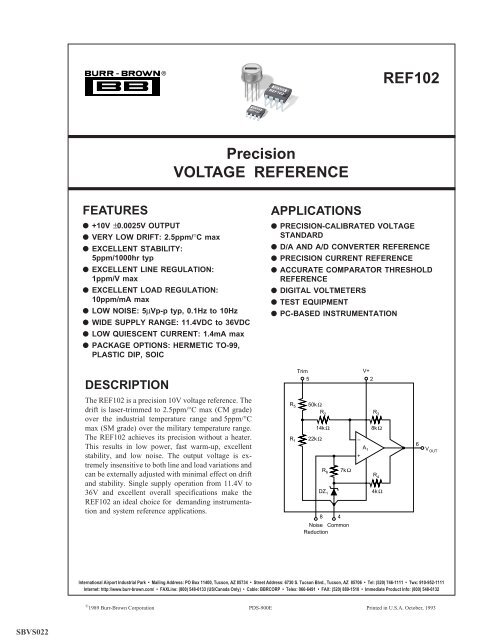
REF102 Precision VOLTAGE REFERENCE
REF102 Precision VOLTAGE REFERENCE
REF102 Precision VOLTAGE REFERENCE

Create successful ePaper yourself
Turn your PDF publications into a flip-book with our unique Google optimized e-Paper software.
<strong>REF102</strong><br />
<strong>REF102</strong><br />
®<br />
<strong>REF102</strong><br />
<strong>Precision</strong><br />
<strong>VOLTAGE</strong> <strong>REFERENCE</strong><br />
FEATURES<br />
● +10V ±0.0025V OUTPUT<br />
● VERY LOW DRIFT: 2.5ppm/°C max<br />
● EXCELLENT STABILITY:<br />
5ppm/1000hr typ<br />
● EXCELLENT LINE REGULATION:<br />
1ppm/V max<br />
● EXCELLENT LOAD REGULATION:<br />
10ppm/mA max<br />
● LOW NOISE: 5µVp-p typ, 0.1Hz to 10Hz<br />
● WIDE SUPPLY RANGE: 11.4VDC to 36VDC<br />
● LOW QUIESCENT CURRENT: 1.4mA max<br />
● PACKAGE OPTIONS: HERMETIC TO-99,<br />
PLASTIC DIP, SOIC<br />
APPLICATIONS<br />
● PRECISION-CALIBRATED <strong>VOLTAGE</strong><br />
STANDARD<br />
● D/A AND A/D CONVERTER <strong>REFERENCE</strong><br />
● PRECISION CURRENT <strong>REFERENCE</strong><br />
● ACCURATE COMPARATOR THRESHOLD<br />
<strong>REFERENCE</strong><br />
● DIGITAL VOLTMETERS<br />
● TEST EQUIPMENT<br />
● PC-BASED INSTRUMENTATION<br />
DESCRIPTION<br />
Trim<br />
V+<br />
5 2<br />
The <strong>REF102</strong> is a precision 10V voltage reference. The<br />
drift is laser-trimmed to 2.5ppm/°C max (CM grade)<br />
over the industrial temperature range and 5ppm/°C<br />
max (SM grade) over the military temperature range.<br />
The <strong>REF102</strong> achieves its precision without a heater.<br />
This results in low power, fast warm-up, excellent<br />
stability, and low noise. The output voltage is extremely<br />
insensitive to both line and load variations and<br />
can be externally adjusted with minimal effect on drift<br />
and stability. Single supply operation from 11.4V to<br />
36V and excellent overall specifications make the<br />
<strong>REF102</strong> an ideal choice for demanding instrumentation<br />
and system reference applications.<br />
R 5 50k Ω<br />
R 2 R 3<br />
14k Ω<br />
8k Ω<br />
R 1 22k Ω<br />
–<br />
A1<br />
+<br />
R 6<br />
DZ 1<br />
8 4<br />
7k Ω<br />
Noise Common<br />
Reduction<br />
R 4<br />
4k Ω<br />
6<br />
V OUT<br />
International Airport Industrial Park • Mailing Address: PO Box 11400, Tucson, AZ 85734 • Street Address: 6730 S. Tucson Blvd., Tucson, AZ 85706 • Tel: (520) 746-1111 • Twx: 910-952-1111<br />
Internet: http://www.burr-brown.com/ • FAXLine: (800) 548-6133 (US/Canada Only) • Cable: BBRCORP • Telex: 066-6491 • FAX: (520) 889-1510 • Immediate Product Info: (800) 548-6132<br />
© 1989 Burr-Brown Corporation PDS-900E Printed in U.S.A. October, 1993<br />
SBVS022
SPECIFICATIONS<br />
ELECTRICAL<br />
At T A = +25°C and V S = +15V power supply, unless otherwise noted.<br />
<strong>REF102</strong>A, R <strong>REF102</strong>B, S <strong>REF102</strong>C, M<br />
PARAMETER CONDITIONS MIN TYP MAX MIN TYP MAX MIN TYP MAX UNITS<br />
OUTPUT <strong>VOLTAGE</strong><br />
Initial T A = 25°C 9.99 10.01 9.995 10.005 9.9975 10.0025 V<br />
vs Temperature (1) 10 5 2.5 ppm/°C<br />
vs Supply<br />
(Line Regulation) V S = 11.4V to 36V 2 1 1 ppm/V<br />
vs Output Current<br />
(Load Regulation) I L = 0mA to +10mA 20 10 10 ppm/mA<br />
I L = 0mA to –5mA 40 20 20 ppm/mA<br />
vs Time T A = 25°<br />
M Package 5 ✻ ✻ ppm/1000hr<br />
P, U Packages (2) 20 ✻ ppm/1000hr<br />
Trim Range (3) ±3 ✻ ✻ %<br />
Capacitive Load, max 1000 ✻ ✻ pF<br />
NOISE (0.1Hz to 10Hz) 5 ✻ ✻ µVp-p<br />
OUTPUT CURRENT +10, –5 ✻ ✻ mA<br />
INPUT <strong>VOLTAGE</strong><br />
RANGE +11.4 +36 ✻ ✻ ✻ ✻ V<br />
QUIESCENT CURRENT (I OUT = 0) +1.4 ✻ ✻ mA<br />
WARM-UP TIME (4) (To 0.1%) 15 ✻ ✻ µs<br />
TEMPERATURE<br />
RANGE<br />
Specification<br />
<strong>REF102</strong>A, B, C –25 +85 ✻ ✻ ✻ ✻ °C<br />
<strong>REF102</strong>R, S –55 +125 ✻ ✻ °C<br />
✻ Specifications same as <strong>REF102</strong>A/R.<br />
NOTES: (1) The “box” method is used to specify output voltage drift vs temperature. See the Discussion of Performance section. (2) Typically 5ppm/1000hrs after 168hr<br />
powered stabilization. (3) Trimming the offset voltage affects drift slightly. See Installation and Operating Instructions for details. (4) With noise reduction pin floating.<br />
See Typical Performance Curves for details.<br />
The information provided herein is believed to be reliable; however, BURR-BROWN assumes no responsibility for inaccuracies or omissions. BURR-BROWN assumes<br />
no responsibility for the use of this information, and all use of such information shall be entirely at the user’s own risk. Prices and specifications are subject to change<br />
without notice. No patent rights or licenses to any of the circuits described herein are implied or granted to any third party. BURR-BROWN does not authorize or warrant<br />
any BURR-BROWN product for use in life support devices and/or systems.<br />
®<br />
<strong>REF102</strong><br />
2
ORDERING INFORMATION<br />
TEMPERATURE MAX INITIAL MAX DRIFT<br />
PRODUCT PACKAGE RANGE ERROR (mV) (ppm/°C)<br />
<strong>REF102</strong>AU 8-Pin SOIC –25°C to +85°C ±10 ±10<br />
<strong>REF102</strong>AP 8-Pin Plastic DIP –25°C to +85°C ±10 ±10<br />
<strong>REF102</strong>BP 8-Pin Plastic DIP –25°C to +85°C ±5 ±5<br />
<strong>REF102</strong>AM Metal TO-99 –25°C to +85°C ±10 ±10<br />
<strong>REF102</strong>BM Metal TO-99 –25°C to +85°C ±5 ±5<br />
<strong>REF102</strong>CM Metal TO-99 –25°C to +85°C ±2.5 ±2.5<br />
<strong>REF102</strong>RM Metal TO-99 –55°C to +125°C ±10 ±10<br />
<strong>REF102</strong>SM Metal TO-99 –55°C to +125°C ±5 ±5<br />
PIN CONFIGURATIONS<br />
ABSOLUTE MAXIMUM RATINGS<br />
Top View<br />
NC<br />
V+<br />
NC<br />
Com<br />
1<br />
2<br />
3<br />
4<br />
8<br />
7<br />
6<br />
5<br />
DIP/SOIC<br />
Noise Reduction<br />
NC<br />
V OUT<br />
Trim<br />
Input Voltage ...................................................................................... +40V<br />
Operating Temperature<br />
P,U .................................................................................. –25°C to +85°C<br />
M ................................................................................... –55°C to +125°C<br />
Storage Temperature Range<br />
P,U .................................................................................. –40°C to +85°C<br />
M ................................................................................... –65°C to +150°C<br />
Lead Temperature (soldering, 10s) ................................................ +300°C<br />
(SOIC, 3s) ....................................................... +260°C<br />
Short-Circuit Protection to Common or V+ ............................... Continuous<br />
Top View<br />
V+<br />
NC<br />
NC<br />
Noise Reduction<br />
1<br />
3<br />
8<br />
4<br />
7<br />
2 6<br />
Common<br />
5<br />
NC<br />
V OUT<br />
Trim<br />
TO-99<br />
ELECTROSTATIC<br />
DISCHARGE SENSITIVITY<br />
This integrated circuit can be damaged by ESD. Burr-Brown<br />
recommends that all integrated circuits be handled with<br />
appropriate precautions. Failure to observe proper handling<br />
and installation procedures can cause damage.<br />
ESD damage can range from subtle performance degradation<br />
to complete device failure. <strong>Precision</strong> integrated circuits may<br />
be more susceptible to damage because very small parametric<br />
changes could cause the device not to meet its published<br />
specifications.<br />
PACKAGE INFORMATION<br />
PACKAGE DRAWING<br />
PRODUCT PACKAGE NUMBER (1)<br />
<strong>REF102</strong>AU 8-Pin SOIC 182<br />
<strong>REF102</strong>AP 8-Pin Plastic DIP 006<br />
<strong>REF102</strong>BP 8-Pin Plastic DIP 006<br />
<strong>REF102</strong>AM Metal-TO-99 001<br />
<strong>REF102</strong>BM Metal-TO-99 001<br />
<strong>REF102</strong>CM Metal-TO-99 001<br />
<strong>REF102</strong>RM Metal-TO-99 001<br />
<strong>REF102</strong>SM Metal-TO-99 001<br />
NOTE: (1) For detailed drawing and dimension table, please see end of data<br />
sheet, or Appendix C of Burr-Brown IC Data Book.<br />
3<br />
<strong>REF102</strong><br />
®
TYPICAL PERFORMANCE CURVES<br />
At T A = +25°C, V S = +15V, unless otherwise noted.<br />
POWER TURN-ON RESPONSE<br />
POWER TURN-ON RESPONSE with 1µF Cn<br />
V OUT<br />
FPO<br />
V OUT<br />
FPO<br />
FPO<br />
V IN<br />
V IN<br />
Time (5µs/div)<br />
Power Turn-On<br />
Time (10ms/div)<br />
Power Turn-On<br />
130<br />
POWER SUPPLY REJECTION vs FREQUENCY<br />
+1.5<br />
LOAD REGULATION<br />
Power Supply Rejection (dB)<br />
120<br />
110<br />
100<br />
90<br />
80<br />
70<br />
Output Voltage Change (mV)<br />
+1.0<br />
+0.5<br />
0<br />
–0.5<br />
–1.0<br />
60<br />
1 100 1k 10k<br />
Frequency (Hz)<br />
–1.5<br />
–5 0 +5 +10<br />
Output Current (mA)<br />
+600<br />
RESPONSE TO THERMAL SHOCK<br />
1.6<br />
QUIESCENT CURRENT vs TEMPERATURE<br />
Output Voltage Change (µV)<br />
+300<br />
0<br />
–300<br />
T A =<br />
+25°C<br />
–600<br />
0<br />
<strong>REF102</strong>CM Immersed in +85°C Fluorinert Bath<br />
T A = +85°C<br />
15<br />
30 45 60<br />
Time (s)<br />
Quiescent Current (mA)<br />
1.4<br />
1.2<br />
1.0<br />
0.8<br />
–75<br />
–50 –25 0 +25 +50 +75 +100 +125<br />
Temperature (°C)<br />
®<br />
<strong>REF102</strong><br />
4
TYPICAL PERFORMANCE CURVES (CONT)<br />
At T A = +25°C, V S = +15V, unless otherwise noted.<br />
TYPICAL <strong>REF102</strong> <strong>REFERENCE</strong> NOISE<br />
Noise Voltage (µV)<br />
6<br />
4<br />
2<br />
0<br />
–2<br />
–4<br />
–6<br />
F P O<br />
20Ω<br />
100µF<br />
DUT<br />
15.8kΩ<br />
Noise Test Circuit.<br />
–<br />
2kΩ<br />
OPA27<br />
+<br />
8KΩ<br />
2µF<br />
Gain = 100V/V<br />
f –3dB = 0.1Hz and 10Hz<br />
Oscilloscope<br />
Low Frequency Noise (1s /div)<br />
(See Noise Test Circuit)<br />
5<br />
<strong>REF102</strong><br />
®
THEORY OF OPERATION<br />
Refer to the diagram on the first page of this data sheet. The<br />
10V output is derived from a compensated buried zener<br />
diode DZ 1 , op amp A 1 , and resistor network R 1 –R 6 .<br />
Approximately 8.2V is applied to the non-inverting input of<br />
A 1 by DZ 1 . R 1 , R 2 , and R 3 are laser-trimmed to produce an<br />
exact 10V output. The zener bias current is established from<br />
the regulated output voltage through R 4 . R 5 allows usertrimming<br />
of the output voltage by providing for small<br />
external adjustment of the amplifier gain. Because the TCR<br />
of R 5 closely matches the TCR of R 1 , R 2 and R 3 , the voltage<br />
trim has minimal effect on the reference drift. The output<br />
voltage noise of the <strong>REF102</strong> is dominated by the noise of the<br />
zener diode. A capacitor can be connected between the<br />
Noise Reduction pin and ground to form a low-pass filter<br />
with R 6 and roll off the high-frequency noise of the zener.<br />
DISCUSSION<br />
OF PERFORMANCE<br />
The <strong>REF102</strong> is designed for applications requiring a precision<br />
voltage reference where both the initial value at room<br />
temperature and the drift over temperature are of importance<br />
to the user. Two basic methods of specifying voltage reference<br />
drift versus temperature are in common usage in the<br />
industry—the “butterfly method” and the “box method.”<br />
The <strong>REF102</strong> is specified with the more commonly used<br />
“box method.” The “box” is formed by the high and low<br />
specification temperatures and a diagonal, the slope of<br />
which is equal to the maximum specified drift.<br />
Since the shape of the actual drift curve is not known, the<br />
vertical position of the box is not exactly known either. It is,<br />
however, bounded by V UPPER BOUND and V LOWER BOUND (see<br />
Figure 1). Figure 1 uses the <strong>REF102</strong>CM as an example. It<br />
has a drift specification of 2.5ppm/°C maximum and a<br />
specification temperature range of –25°C to +85°C. The<br />
“box” height, V 1 to V 2 , is 2.75mV.<br />
Output Voltage (V)<br />
+10.00275<br />
V 1<br />
V NOMINAL<br />
+10.0000<br />
V 2<br />
+9.99725<br />
<strong>REF102</strong>BM V UPPER BOUND<br />
<strong>REF102</strong>BM V LOWER BOUND<br />
–25 0 +25 +50 +85<br />
Temperature (°C)<br />
FIGURE 1. <strong>REF102</strong>CM Output Voltage Drift.<br />
2.75mV<br />
Worst-case<br />
∆V OUT<br />
for<br />
<strong>REF102</strong>CM<br />
INSTALLATION AND<br />
OPERATING INSTRUCTIONS<br />
BASIC CIRCUIT CONNECTION<br />
Figure 2 shows the proper connection of the <strong>REF102</strong>. To<br />
achieve the specified performance, pay careful attention to<br />
layout. A low resistance star configuration will reduce voltage<br />
errors, noise pickup, and noise coupled from the power<br />
supply. Commons should be connected as indicated being<br />
sure to minimize interconnection resistances.<br />
V+<br />
+ 1µF<br />
Tantalum<br />
NOTES: (1) Lead resistances here of up to a few ohms have negligible<br />
effect on performance. (2) A resistance of 0.1Ω in series with these<br />
leads will cause a 1mV error when the load current is at its maximum of<br />
10mA. This results in a 0.01% error of 10V.<br />
FIGURE 2. <strong>REF102</strong> Installation.<br />
OPTIONAL OUTPUT <strong>VOLTAGE</strong> ADJUSTMENT<br />
Optional output voltage adjustment circuits are shown in<br />
Figures 3 and 4. Trimming the output voltage will change<br />
the voltage drift by approximately 0.008ppm/°C per mV of<br />
trimmed voltage. In the circuit in Figure 3, any mismatch in<br />
TCR between the two sections of the potentiometer will also<br />
affect drift, but the effect of the ∆TCR is reduced by a factor<br />
of five by the internal resistor divider. A high quality<br />
potentiometer, with good mechanical stability, such as a<br />
cermet, should be used. The circuit in Figure 3 has a<br />
minimum trim range of ±300mV. The circuit in Figure 4 has<br />
less range but provides higher resolution. The mismatch in<br />
TCR between R S and the internal resistors can introduce<br />
some slight drift. This effect is minimized if R S is kept<br />
significantly larger than the 50kΩ internal resistor. A TCR<br />
of 100ppm/°C is normally sufficient.<br />
<strong>REF102</strong><br />
4<br />
V+<br />
2<br />
V OUT<br />
6<br />
(1)<br />
V TRIM<br />
5<br />
<strong>REF102</strong><br />
4<br />
(1)<br />
2 (2)<br />
R L 1 R L 2 R L 3<br />
Minimum range (±300mV) and minimal<br />
degradation of drift.<br />
6<br />
+ 1µF<br />
Tantalum<br />
20kΩ<br />
Output<br />
Voltage<br />
Adjust<br />
(2)<br />
+10V<br />
FIGURE 3. <strong>REF102</strong> Optional Output Voltage Adjust.<br />
®<br />
<strong>REF102</strong><br />
6
<strong>REF102</strong><br />
4<br />
V+<br />
2<br />
V OUT<br />
6<br />
V TRIM<br />
5<br />
R S<br />
1M Ω<br />
FIGURE 4. <strong>REF102</strong> Optional Output Voltage Fine Adjust.<br />
OPTIONAL NOISE REDUCTION<br />
+ 1µF<br />
Tantalum<br />
20kΩ<br />
Output<br />
Voltage<br />
Adjust<br />
+10V<br />
The high-frequency noise of the <strong>REF102</strong> is dominated by<br />
the zener diode noise. This noise can be greatly reduced by<br />
connecting a capacitor between the Noise Reduction pin and<br />
ground. The capacitor forms a low pass filter with R 6 (refer<br />
to the figure on the first page of the data sheet) and attenuates<br />
the high-frequency noise generated by the zener. Figure<br />
5 shows the effect of a 1µF noise reduction capacitor on the<br />
high frequency noise of the <strong>REF102</strong>. R 6 is typically 7kΩ so<br />
the filter has a –3dB frequency of about 22Hz. The result is<br />
a reduction in noise from about 800µVp-p to under 200µ<br />
Vp-p. If further noise reduction is required, use the circuit in<br />
Figure 14.<br />
APPLICATIONS INFORMATION<br />
High accuracy, extremely low drift, outstanding stability,<br />
and low cost make the <strong>REF102</strong> an ideal choice for all<br />
instrumentation and system reference applications. Figures 6<br />
through 14 show a variety of useful application circuits.<br />
6<br />
<strong>REF102</strong><br />
1.4mA < (5V –I<br />
Higher resolution, reduced range (typically ±25mV).<br />
L<br />
) < 5.4mA<br />
R S<br />
4<br />
–10V Out<br />
I<br />
R L<br />
S<br />
–15V<br />
V+ (1.4V to 26V)<br />
2<br />
a) Resister Biased –10V Reference<br />
R 1<br />
<strong>REF102</strong><br />
2kΩ<br />
6<br />
10V<br />
C 1<br />
1000pF<br />
4<br />
OPA27<br />
–10V Out<br />
b) <strong>Precision</strong> –10V Reference.<br />
See AB-004 for more detail<br />
NO C N<br />
2<br />
V+ (1.4V to 26V)<br />
FIGURE 6. –10V Reference Using a) Resistor or b) OPA27.<br />
C N = 1µF<br />
FIGURE 5. Effect of 1µF Noise Reduction Capacitor on<br />
Broadband Noise (f –3dB = 1MHz).<br />
7<br />
<strong>REF102</strong><br />
®
V+<br />
2<br />
V+<br />
V+<br />
<strong>REF102</strong><br />
6<br />
–<br />
OPA27<br />
+<br />
+10V<br />
220Ω<br />
2<br />
2N2905<br />
2<br />
R 1<br />
= V CC<br />
– 10V<br />
4<br />
I L<br />
6<br />
<strong>REF102</strong><br />
I L<br />
+10V<br />
<strong>REF102</strong><br />
6<br />
I L<br />
I L (TYP)<br />
+10V<br />
a) –20mA < I L<br />
< +20mA<br />
(OPA27 also improves transient immunity)<br />
4<br />
b) –5mA < I L<br />
< +100mA<br />
4<br />
c) I L (MAX)<br />
= I L (TYP)<br />
+10mA<br />
I L (MIN)<br />
= I L (TYP)<br />
–5mA<br />
FIGURE 7. +10V Reference With Output Current Boosted to: a) ±20mA, b) +100mA, and c) I L (TYP) +10mA, –5A.<br />
+15V<br />
2<br />
6<br />
357Ω<br />
1/2W<br />
28mA<br />
28.5mA<br />
+5V<br />
<strong>REF102</strong><br />
350 Ω Strain<br />
Gauge Bridge<br />
4<br />
6<br />
–<br />
OPA27<br />
2<br />
R G<br />
5<br />
10<br />
–<br />
INA101<br />
+<br />
8<br />
VOUT<br />
x100<br />
+<br />
3<br />
–15V<br />
–5V<br />
357Ω<br />
1/2W<br />
FIGURE 8. Strain Gauge Conditioner for 350Ω Bridge.<br />
V+<br />
2<br />
V+<br />
2<br />
<strong>REF102</strong><br />
4<br />
6<br />
2<br />
3<br />
25kΩ<br />
25kΩ<br />
25kΩ<br />
5<br />
6<br />
+10V<br />
Out<br />
–10V<br />
Out<br />
<strong>REF102</strong><br />
4<br />
6<br />
OPA111<br />
–<br />
+<br />
R<br />
I OUT<br />
LOAD<br />
25kΩ<br />
1<br />
See AB-005 for more details.<br />
INA105<br />
I OUT<br />
= 10V , R ≥ 1kΩ<br />
R<br />
See AB-002 for more details and I Sink Circuit.<br />
Can be connected<br />
to ground or –V . S<br />
FIGURE 9. ±10V Reference.<br />
FIGURE 10. Positive <strong>Precision</strong> Current Source.<br />
®<br />
<strong>REF102</strong><br />
8
31.4V to 56V<br />
2<br />
2<br />
V+<br />
6 +10V<br />
<strong>REF102</strong><br />
6<br />
+30V<br />
<strong>REF102</strong><br />
INA105<br />
2<br />
2<br />
<strong>REF102</strong><br />
6<br />
4<br />
+20V<br />
4<br />
3<br />
–<br />
+<br />
5<br />
6<br />
+5V<br />
1<br />
2<br />
4<br />
<strong>REF102</strong><br />
6<br />
+10V<br />
FIGURE 13. +5V and +10V Reference.<br />
V+<br />
4<br />
2<br />
NOTES: (1) <strong>REF102</strong>s can be stacked to obtain voltages in multiples of 10V.<br />
(2) The supply voltage should be between 10n + 1.4 and 10n + 26 where n<br />
is the number of <strong>REF102</strong>s. (3) Output current of each <strong>REF102</strong> must not<br />
exceed its rated output current of +10, –5mA. This includes the current<br />
delivered to the lower <strong>REF102</strong>.<br />
<strong>REF102</strong><br />
(1)<br />
4<br />
2kΩ<br />
6<br />
V OUT 1<br />
R2<br />
2kΩ<br />
FIGURE 11. Stacked References.<br />
C 2<br />
2<br />
2<br />
V+<br />
<strong>REF102</strong><br />
6 +5V<br />
Out<br />
2<br />
<strong>REF102</strong><br />
(2)<br />
4<br />
V+<br />
2<br />
–<br />
1µF<br />
2kΩ<br />
OPA27<br />
6<br />
3<br />
+<br />
R1<br />
V OUT 2 1k Ω<br />
+10V<br />
C<br />
VREF<br />
1 1µF<br />
INA105<br />
5<br />
4<br />
–5V<br />
Out<br />
V+<br />
2<br />
–<br />
+<br />
6<br />
<strong>REF102</strong><br />
(N)<br />
2kΩ<br />
6<br />
V OUT N<br />
V REF<br />
= (V O1<br />
+ V O2<br />
....V OUT N<br />
)<br />
N<br />
e N<br />
= 5µVp-p (f = 0.1Hz to 1Mhz)<br />
1 3<br />
4<br />
N<br />
See AB-003 for more details.<br />
FIGURE 12. ±5V Reference.<br />
FIGURE 14. <strong>Precision</strong> Voltage Reference with Extremely<br />
Low Noise.<br />
9<br />
<strong>REF102</strong><br />
®
IMPORTANT NOTICE<br />
Texas Instruments and its subsidiaries (TI) reserve the right to make changes to their products or to discontinue<br />
any product or service without notice, and advise customers to obtain the latest version of relevant information<br />
to verify, before placing orders, that information being relied on is current and complete. All products are sold<br />
subject to the terms and conditions of sale supplied at the time of order acknowledgment, including those<br />
pertaining to warranty, patent infringement, and limitation of liability.<br />
TI warrants performance of its semiconductor products to the specifications applicable at the time of sale in<br />
accordance with TI’s standard warranty. Testing and other quality control techniques are utilized to the extent<br />
TI deems necessary to support this warranty. Specific testing of all parameters of each device is not necessarily<br />
performed, except those mandated by government requirements.<br />
Customers are responsible for their applications using TI components.<br />
In order to minimize risks associated with the customer’s applications, adequate design and operating<br />
safeguards must be provided by the customer to minimize inherent or procedural hazards.<br />
TI assumes no liability for applications assistance or customer product design. TI does not warrant or represent<br />
that any license, either express or implied, is granted under any patent right, copyright, mask work right, or other<br />
intellectual property right of TI covering or relating to any combination, machine, or process in which such<br />
semiconductor products or services might be or are used. TI’s publication of information regarding any third<br />
party’s products or services does not constitute TI’s approval, warranty or endorsement thereof.<br />
Copyright © 2000, Texas Instruments Incorporated