BTS7960 datasheet - DFRobot
BTS7960 datasheet - DFRobot
BTS7960 datasheet - DFRobot

Create successful ePaper yourself
Turn your PDF publications into a flip-book with our unique Google optimized e-Paper software.
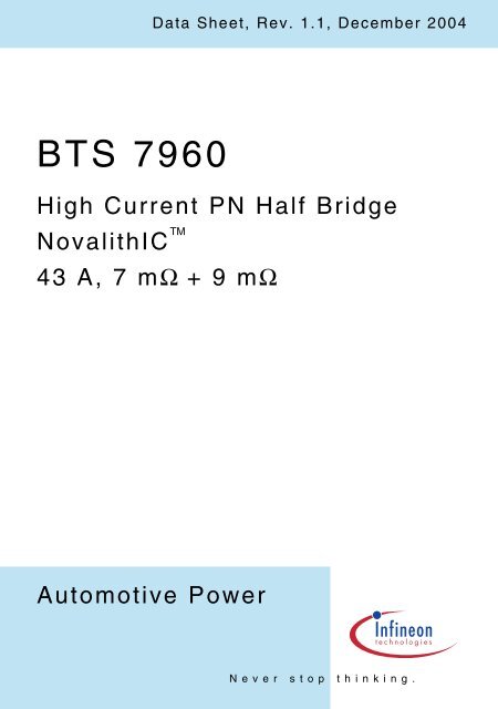
Data Sheet, Rev. 1.1, December 2004<br />
BTS 7960<br />
High Current PN Half Bridge<br />
NovalithIC<br />
TM<br />
43 A, 7 mΩ + 9 mΩ<br />
Automotive Power<br />
Never stop thinking.
High Current PN Half Bridge<br />
BTS 7960<br />
Product Summary . . . . . . . . . . . . . . . . . . . . . . . . . . . . . . . . . . . . . . . . . . . . . . . . . . . .2<br />
Basic Features . . . . . . . . . . . . . . . . . . . . . . . . . . . . . . . . . . . . . . . . . . . . . . . . . . . . . . .2<br />
1Overview . . . . . . . . . . . . . . . . . . . . . . . . . . . . . . . . . . . . . . . . . . . . . . . . . . . . . . . . .3<br />
1.1 Block Diagram . . . . . . . . . . . . . . . . . . . . . . . . . . . . . . . . . . . . . . . . . . . . . . . . . . .3<br />
1.2 Terms . . . . . . . . . . . . . . . . . . . . . . . . . . . . . . . . . . . . . . . . . . . . . . . . . . . . . . . . .4<br />
2 Pin Configuration . . . . . . . . . . . . . . . . . . . . . . . . . . . . . . . . . . . . . . . . . . . . . . . . . .5<br />
2.1 Pin Assignment . . . . . . . . . . . . . . . . . . . . . . . . . . . . . . . . . . . . . . . . . . . . . . . . . .5<br />
2.2 Pin Definitions and Functions . . . . . . . . . . . . . . . . . . . . . . . . . . . . . . . . . . . . . . .5<br />
3 Maximum Ratings . . . . . . . . . . . . . . . . . . . . . . . . . . . . . . . . . . . . . . . . . . . . . . . . . .6<br />
4 Block Description and Characteristics . . . . . . . . . . . . . . . . . . . . . . . . . . . . . . . . .7<br />
4.1 Supply Characteristics . . . . . . . . . . . . . . . . . . . . . . . . . . . . . . . . . . . . . . . . . . . . .7<br />
4.2 Power Stages . . . . . . . . . . . . . . . . . . . . . . . . . . . . . . . . . . . . . . . . . . . . . . . . . . .8<br />
4.2.1 Power Stages - Static Characteristics . . . . . . . . . . . . . . . . . . . . . . . . . . . . 9<br />
4.2.2 Switching Times . . . . . . . . . . . . . . . . . . . . . . . . . . . . . . . . . . . . . . . . . . . 10<br />
4.2.3 Power Stages - Dynamic Characteristics . . . . . . . . . . . . . . . . . . . . . . . . 11<br />
4.3 Protection Functions . . . . . . . . . . . . . . . . . . . . . . . . . . . . . . . . . . . . . . . . . . . . .13<br />
4.3.1 Overvoltage Lock Out . . . . . . . . . . . . . . . . . . . . . . . . . . . . . . . . . . . . . . . 13<br />
4.3.2 Undervoltage Shut Down . . . . . . . . . . . . . . . . . . . . . . . . . . . . . . . . . . . . . 13<br />
4.3.3 Overtemperature Protection . . . . . . . . . . . . . . . . . . . . . . . . . . . . . . . . . . 13<br />
4.3.4 Current Limitation . . . . . . . . . . . . . . . . . . . . . . . . . . . . . . . . . . . . . . . . . . 13<br />
4.3.5 Short Circuit Protection . . . . . . . . . . . . . . . . . . . . . . . . . . . . . . . . . . . . . . 15<br />
4.3.6 Electrical Characteristics - Protection Functions . . . . . . . . . . . . . . . . . . . 16<br />
4.4 Control and Diagnostics . . . . . . . . . . . . . . . . . . . . . . . . . . . . . . . . . . . . . . . . . .17<br />
4.4.1 Input Circuit . . . . . . . . . . . . . . . . . . . . . . . . . . . . . . . . . . . . . . . . . . . . . . . 17<br />
4.4.2 Dead Time Generation . . . . . . . . . . . . . . . . . . . . . . . . . . . . . . . . . . . . . . 17<br />
4.4.3 Adjustable Slew Rate . . . . . . . . . . . . . . . . . . . . . . . . . . . . . . . . . . . . . . . 17<br />
4.4.4 Status Flag Diagnosis With Current Sense Capability . . . . . . . . . . . . . . 17<br />
4.4.5 Truth Table . . . . . . . . . . . . . . . . . . . . . . . . . . . . . . . . . . . . . . . . . . . . . . . 19<br />
4.4.6 Electrical Characteristics - Control and Diagnostics . . . . . . . . . . . . . . . . 20<br />
5 Thermal Characteristics . . . . . . . . . . . . . . . . . . . . . . . . . . . . . . . . . . . . . . . . . . . .21<br />
6 Application . . . . . . . . . . . . . . . . . . . . . . . . . . . . . . . . . . . . . . . . . . . . . . . . . . . . . . .22<br />
6.1 Application Example . . . . . . . . . . . . . . . . . . . . . . . . . . . . . . . . . . . . . . . . . . . . .22<br />
6.2 Layout Considerations . . . . . . . . . . . . . . . . . . . . . . . . . . . . . . . . . . . . . . . . . . . .22<br />
7 Package Outlines P-TO-263-7 . . . . . . . . . . . . . . . . . . . . . . . . . . . . . . . . . . . . . . .23<br />
8 Package Outlines P-TO-220-7 . . . . . . . . . . . . . . . . . . . . . . . . . . . . . . . . . . . . . . .24<br />
9 Revision History . . . . . . . . . . . . . . . . . . . . . . . . . . . . . . . . . . . . . . . . . . . . . . . . . .25<br />
Data Sheet 1 Rev. 1.1, 2004-12-07
High Current PN Half Bridge<br />
TM<br />
NovalithIC<br />
BTS 7960B<br />
BTS 7960P<br />
Product Summary<br />
The BTS 7960 is a fully integrated high current half<br />
bridge for motor drive applications. It is part of the<br />
NovalithIC TM family containing one p-channel highside<br />
MOSFET and one n-channel lowside MOSFET with an<br />
integrated driver IC in one package. Due to the p-channel<br />
highside switch the need for a charge pump is eliminated<br />
thus minimizing EMI. Interfacing to a microcontroller is<br />
made easy by the integrated driver IC which features<br />
logic level inputs, diagnosis with current sense, slew rate<br />
adjustment, dead time generation and protection against<br />
overtemperature, overvoltage, undervoltage,<br />
overcurrent and short circuit.<br />
The BTS 7960 provides a cost optimized solution for<br />
protected high current PWM motor drives with very low<br />
board space consumption.<br />
BTS 7960B<br />
P-TO-263-7<br />
BTS 7960P<br />
P-TO-220-7<br />
Basic Features<br />
• Path resistance of typ. 16 mΩ @25°C<br />
• Low quiescent current of typ. 7 µA @ 25 °C<br />
• PWM capability of up to 25 kHz combined with active freewheeling<br />
• Switched mode current limitation for reduced power dissipation in overcurrent<br />
• Current limitation level of 43 A typ.<br />
• Status flag diagnosis with current sense capability<br />
• Overtemperature shut down with latch behaviour<br />
• Overvoltage lock out<br />
• Undervoltage shut down<br />
• Driver circuit with logic level inputs<br />
• Adjustable slew rates for optimized EMI<br />
Type Ordering Code Package<br />
BTS 7960B Q67060-S6160 P-TO-263-7<br />
BTS 7960P on request P-TO-220-7<br />
Data Sheet 2 Rev. 1.1, 2004-12-07
1 Overview<br />
High Current PN Half Bridge<br />
BTS 7960<br />
Overview<br />
The BTS 7960 is part of the NovalithIC family containing three separate chips in one<br />
package: One p-channel highside MOSFET and one n-channel lowside MOSFET<br />
together with a driver IC, forming a fully integrated high current half-bridge. All three<br />
chips are mounted on one common leadframe, using the chip on chip and chip by chip<br />
technology. The power switches utilize vertical MOS technologies to ensure optimum on<br />
state resistance. Due to the p-channel highside switch the need for a charge pump is<br />
eliminated thus minimizing EMI. Interfacing to a microcontroller is made easy by the<br />
integrated driver IC which features logic level inputs, diagnosis with current sense, slew<br />
rate adjustment, dead time generation and protection against overtemperature,<br />
overvoltage, undervoltage, overcurrent and short circuit. The BTS 7960 can be<br />
combined with other BTS 7960 to form H-bridge and 3-phase drive configurations.<br />
1.1 Block Diagram<br />
BTS 7960<br />
HS base-chip<br />
VS<br />
Top-chip<br />
IN<br />
INH<br />
SR<br />
IS<br />
Gate Driver<br />
Dead Time Gen.<br />
Slew Rate Adj.<br />
UV Shut Down<br />
OV Lock Out<br />
OT Shut Down<br />
Current Lim.<br />
Diagnosis<br />
Current Sense<br />
LS base-chip<br />
OUT<br />
GND<br />
Figure 1<br />
Block Diagram<br />
Data Sheet 3 Rev. 1.1, 2004-12-07
1.2 Terms<br />
Following figure shows the terms used in this data sheet.<br />
High Current PN Half Bridge<br />
BTS 7960<br />
Overview<br />
I IN<br />
V IN<br />
V INH<br />
V SR<br />
I INH<br />
I SR<br />
V VS<br />
,V S<br />
I OUT<br />
, I L<br />
V OUT<br />
I VS<br />
, -I D(HS)<br />
V DS(HS)<br />
IN<br />
VS<br />
INH<br />
SR<br />
BTS 7960<br />
OUT<br />
V SD(LS)<br />
V IS<br />
I IS<br />
IS<br />
GND<br />
I GND,<br />
I D(LS)<br />
Figure 2<br />
Terms<br />
Data Sheet 4 Rev. 1.1, 2004-12-07
High Current PN Half Bridge<br />
BTS 7960<br />
Pin Configuration<br />
2 Pin Configuration<br />
2.1 Pin Assignment<br />
BTS 7960B<br />
P-TO-263-7<br />
BTS 7960P<br />
P-TO-220-7<br />
8<br />
8<br />
1 2<br />
3 5 6<br />
7<br />
4<br />
1 2 4<br />
3 5 6 7<br />
Figure 3<br />
Pin Assignment BTS 7960B and BTS 7960P (top view)<br />
2.2 Pin Definitions and Functions<br />
Pin Symbol I/O Function<br />
1 GND - Ground<br />
2 IN I Input<br />
Defines whether high- or lowside switch is activated<br />
3 INH I Inhibit<br />
When set to low device goes in sleep mode<br />
4,8 OUT O Power output of the bridge<br />
5 SR I Slew Rate<br />
The slew rate of the power switches can be adjusted<br />
by connecting a resistor between SR and GND<br />
6 IS O Current Sense and Diagnosis<br />
7 VS - Supply<br />
Bold type: pin needs power wiring<br />
Data Sheet 5 Rev. 1.1, 2004-12-07
3 Maximum Ratings<br />
High Current PN Half Bridge<br />
BTS 7960<br />
Maximum Ratings<br />
-40 40 1)<br />
-40 °C < T j < 150 °C (unless otherwise specified)<br />
Pos Parameter Symbol Limits Unit Test Condition<br />
min max<br />
Electrical Maximum Ratings<br />
3.0.1 Supply voltage V VS -0.3 45 V<br />
3.0.2 Logic Input Voltage V IN -0.3 5.3 V<br />
V INH<br />
3.0.3 HS/LS continuous drain I D(HS)<br />
A T C < 85°C<br />
current<br />
I D(LS) switch active<br />
3.0.4 HS pulsed drain current I D(HS) -60 60 1) A T C < 85°C<br />
3.0.5 LS pulsed drain current I D(LS) -60 60 1) A t pulse = 10ms<br />
3.0.6 Voltage at SR pin V SR -0.3 1.0 V<br />
3.0.7 Voltage between VS and V VS -V IS -0.3 45 V<br />
IS pin<br />
3.0.8 Voltage at IS pin V IS -20 45 V<br />
Thermal Maximum Ratings<br />
3.0.9 Junction temperature T j -40 150 °C<br />
3.0.10 Storage temperature T stg -55 150 °C<br />
ESD Susceptibility<br />
3.0.11 ESD susceptibility HBM<br />
IN, INH, SR, IS<br />
OUT, GND, VS<br />
V ESD<br />
-2<br />
-6<br />
2<br />
6<br />
kV<br />
according to EIA/<br />
JESD 22-A 114B<br />
1)<br />
Maximum reachable current may be smaller depending on current limitation level<br />
Note: Maximum ratings are absolute ratings; exceeding any one of these values may<br />
cause irreversible damage to the device. Exposure to maximum rating conditions<br />
for extended periods of time may affect device reliability<br />
Data Sheet 6 Rev. 1.1, 2004-12-07
4 Block Description and Characteristics<br />
High Current PN Half Bridge<br />
BTS 7960<br />
Block Description and Characteristics<br />
4.1 Supply Characteristics<br />
– 40 °C < T j < 150 °C, 8 V < V S < 18 V, I L = 0A (unless otherwise specified)<br />
Pos. Parameter Symbol Limit Values Unit Test Conditions<br />
min. typ. max.<br />
General<br />
4.1.1 Operating Voltage V S 5.5 – 27.5 V<br />
4.1.2 Supply Current I VS(on) – 2 3 mA V INH = 5 V<br />
V IN = 0V or 5V<br />
R SR =0 Ω<br />
DC-mode<br />
normal operation<br />
(no fault condition)<br />
4.1.3 Quiescent Current I VS(off) – 7 15 µA V INH = 0 V<br />
V IN = 0V or 5V<br />
T j
High Current PN Half Bridge<br />
BTS 7960<br />
Block Description and Characteristics<br />
4.2 Power Stages<br />
The power stages of the BTS 7960 consist of a p-channel vertical DMOS transistor for<br />
the high side switch and a n-channel vertical DMOS transistor for the low side switch. All<br />
protection and diagnostic functions are located in a separate top chip. Both switches can<br />
be operated up to 25 kHz, allowing active freewheeling and thus minimizing power<br />
dissipation in the forward operation of the integrated diodes.<br />
The on state resistance R ON is dependent on the supply voltage V S as well as on the<br />
junction temperature T j . The typical on state resistance characteristics are shown in<br />
Figure 4.<br />
High Side Switch<br />
Low Side Switch<br />
25<br />
25<br />
mΩ<br />
mΩ<br />
20<br />
20<br />
R ON(HS)<br />
R ON(LS)<br />
15<br />
15<br />
T j<br />
= 150°C<br />
10<br />
T j = 150°C<br />
10<br />
T j<br />
= 25°C<br />
T j<br />
= 25°C<br />
T j<br />
= -40°C<br />
5<br />
4 8 12 16 20 24 V 28<br />
V S<br />
T j<br />
= -40°C<br />
5<br />
4 8 12 16 20 24 V 28<br />
V S<br />
Figure 4<br />
Typical On State Resistance vs. Supply Voltage<br />
Data Sheet 8 Rev. 1.1, 2004-12-07
4.2.1 Power Stages - Static Characteristics<br />
High Current PN Half Bridge<br />
BTS 7960<br />
Block Description and Characteristics<br />
– 40 °C < T j < 150 °C, 8 V < V S < 18 V (unless otherwise specified)<br />
Pos. Parameter Symbol Limit Values Unit Test Conditions<br />
min. typ. max.<br />
High Side Switch - Static Characteristics<br />
4.2.1 On state high side<br />
resistance<br />
4.2.2 Leakage current high<br />
side<br />
4.2.3 Reverse diode<br />
forward-voltage high<br />
side 1)<br />
R ON(HS)<br />
–<br />
–<br />
7<br />
10<br />
9<br />
12.5<br />
mΩ<br />
I OUT = 9 A<br />
V S = 13.5 V<br />
T j = 25 °C<br />
T j = 150 °C<br />
I L(LKHS) – – 1 µA V INH = 0 V<br />
V OUT = 0 V<br />
T j < 85 °C<br />
– – 50 µA V INH = 0 V<br />
V OUT = 0 V<br />
T j = 150 °C<br />
V DS(HS)<br />
–<br />
–<br />
–<br />
Low Side Switch - Static Characteristics<br />
4.2.4 On state low side<br />
resistance<br />
4.2.5 Leakage current low<br />
side<br />
R ON(LS)<br />
–<br />
–<br />
V 4.2.6 Reverse diode<br />
forward-voltage low<br />
side 1) SD(LS)<br />
–<br />
–<br />
–<br />
0.9<br />
0.8<br />
0.6<br />
9<br />
14<br />
1.5<br />
1.1<br />
0.8<br />
12<br />
18<br />
V<br />
mΩ<br />
I OUT =-9A<br />
T j = -40 °C<br />
T j = 25 °C<br />
T j = 150 °C<br />
I OUT =-9A<br />
V S = 13.5V<br />
T j = 25 °C<br />
T j = 150 °C<br />
I L(LKLS) – – 1 µA V INH = 0 V<br />
V OUT = V S<br />
T j < 85 °C<br />
– – 15 µA V INH = 0 V<br />
V OUT = V S<br />
T j = 150 °C<br />
0.9<br />
0.8<br />
0.6<br />
1.5<br />
1.1<br />
0.8<br />
V<br />
I OUT = 9 A<br />
T j = -40 °C<br />
T j = 25 °C<br />
T j = 150 °C<br />
1)<br />
Due to active freewheeling, diode is conducting only for a few µs, depending on R SR<br />
Data Sheet 9 Rev. 1.1, 2004-12-07
High Current PN Half Bridge<br />
BTS 7960<br />
Block Description and Characteristics<br />
4.2.2 Switching Times<br />
IN<br />
t<br />
t dr(HS) t r(HS) t df(HS) t f(HS)<br />
V OUT<br />
90%<br />
∆V OUT<br />
90%<br />
∆V OUT<br />
10%<br />
Figure 5<br />
Definition of switching times high side (R load to GND)<br />
10%<br />
t<br />
IN<br />
t df(LS)<br />
t f(LS)<br />
∆V OUT<br />
∆V OUT<br />
t dr(LS)<br />
t<br />
t r(LS)<br />
V OUT<br />
90%<br />
90%<br />
10%<br />
10%<br />
t<br />
Figure 6<br />
Definition of switching times low side (R load to VS)<br />
Due to the timing differences for the rising and the falling edge there will be a slight<br />
difference between the length of the input pulse and the length of the output pulse. It can<br />
be calculated using the following formulas:<br />
• ∆t HS = (t dr(HS) + 0.5 t r(HS) ) - (t df(HS) + 0.5 t f(HS) )<br />
• ∆t LS = (t df(LS) + 0.5 t f(LS) ) - (t dr(LS) + 0.5 t r(LS) ).<br />
Data Sheet 10 Rev. 1.1, 2004-12-07
4.2.3 Power Stages - Dynamic Characteristics<br />
High Current PN Half Bridge<br />
BTS 7960<br />
Block Description and Characteristics<br />
-40 °C < T j < 150 °C, V S = 13.5 V, R load = 2Ω (unless otherwise specified)<br />
Pos. Parameter Symbol Limit Values Unit Test Conditions<br />
min. typ. max.<br />
HIgh Side Switch Dynamic Characteristics<br />
r(HS)<br />
0.5<br />
–<br />
2.8<br />
4.2.8 Slew rate HS on ∆V OUT /<br />
t r( HS) –<br />
–<br />
–<br />
4.2.9 Switch on delay time<br />
HS<br />
t dr(HS)<br />
1.7<br />
–<br />
5.6<br />
f(HS)<br />
0.5<br />
–<br />
2.8<br />
4.2.11 Slew rate HS off -∆V OUT /<br />
t f(HS) –<br />
–<br />
–<br />
4.2.12 Switch off delay time<br />
HS<br />
t df(HS)<br />
1.2<br />
–<br />
4<br />
1<br />
2<br />
7<br />
11<br />
6<br />
1.6<br />
3.1<br />
4.4<br />
14<br />
1<br />
2<br />
7<br />
11<br />
6<br />
1.6<br />
2.4<br />
3.4<br />
10<br />
1.5<br />
–<br />
11<br />
–<br />
–<br />
–<br />
4.5<br />
–<br />
22.4<br />
1.5<br />
–<br />
11<br />
–<br />
–<br />
–<br />
3.6<br />
–<br />
16<br />
µs<br />
V/µs<br />
µs<br />
µs<br />
V/µs<br />
µs<br />
R SR = 0 Ω<br />
R SR = 5.1 kΩ<br />
R SR = 51 kΩ<br />
R SR = 0 Ω<br />
R SR = 5.1 kΩ<br />
R SR = 51 kΩ<br />
R SR = 0 Ω<br />
R SR = 5.1 kΩ<br />
R SR = 51 kΩ<br />
R SR = 0 Ω<br />
R SR = 5.1 kΩ<br />
R SR = 51 kΩ<br />
R SR = 0 Ω<br />
R SR = 5.1 kΩ<br />
R SR = 51 kΩ<br />
R SR = 0 Ω<br />
R SR = 5.1 kΩ<br />
R SR = 51 kΩ<br />
Data Sheet 11 Rev. 1.1, 2004-12-07
High Current PN Half Bridge<br />
BTS 7960<br />
Block Description and Characteristics<br />
-40 °C < T j < 150 °C, V S = 13.5 V, R load = 2Ω (unless otherwise specified)<br />
Pos. Parameter Symbol Limit Values Unit Test Conditions<br />
min. typ. max.<br />
Low Side Switch Dynamic Characteristics<br />
r(LS)<br />
0.5<br />
–<br />
2.8<br />
1<br />
2<br />
7<br />
1.5<br />
–<br />
11<br />
µs<br />
R SR = 0 Ω<br />
R SR = 5.1 kΩ<br />
R SR = 51 kΩ<br />
4.2.14 Slew rate LS switch off ∆V OUT /<br />
t r(LS) –<br />
–<br />
–<br />
11<br />
6<br />
1.6<br />
–<br />
–<br />
–<br />
V/µs<br />
R SR = 0 Ω<br />
R SR = 5.1 kΩ<br />
R SR = 51 kΩ<br />
4.2.15 Switch off delay time<br />
LS<br />
t dr(LS)<br />
0.7<br />
–<br />
2.8<br />
1.3<br />
2.2<br />
7<br />
1.9<br />
–<br />
11.2<br />
µs<br />
R SR = 0 Ω<br />
R SR = 5.1 kΩ<br />
R SR = 51 kΩ<br />
f(LS)<br />
0.5<br />
–<br />
2.8<br />
1<br />
2<br />
7<br />
1.5<br />
–<br />
11<br />
µs<br />
R SR = 0 Ω<br />
R SR = 5.1 kΩ<br />
R SR = 51 kΩ<br />
4.2.17 Slew rate LS switch on -∆V OUT /<br />
t f(LS) –<br />
–<br />
–<br />
11<br />
6<br />
1.6<br />
–<br />
–<br />
–<br />
V/µs<br />
R SR = 0 Ω<br />
R SR = 5.1 kΩ<br />
R SR = 51 kΩ<br />
4.2.18 Switch on delay time<br />
LS<br />
t df(LS)<br />
2.2<br />
–<br />
6.4<br />
4<br />
5.6<br />
16<br />
5.8<br />
–<br />
25.4<br />
µs<br />
R SR = 0 Ω<br />
R SR = 5.1 kΩ<br />
R SR = 51 kΩ<br />
Data Sheet 12 Rev. 1.1, 2004-12-07
High Current PN Half Bridge<br />
BTS 7960<br />
Block Description and Characteristics<br />
4.3 Protection Functions<br />
The device provides integrated protection functions. These are designed to prevent IC<br />
destruction under fault conditions described in the data sheet. Fault conditions are<br />
considered as “outside” normal operating range. Protection functions are not to be used<br />
for continuous or repetitive operation, with the exception of the current limitation<br />
(Chapter 4.3.4). In a fault condition the BTS 7960 will apply the highest slew rate<br />
possible independent of the connected slew rate resistor. Overvoltage, overtemperature<br />
and overcurrent are indicated by a fault current I IS(LIM) at the IS pin as described in the<br />
paragraph “Status Flag Diagnosis With Current Sense Capability” on Page 17 and<br />
Figure 10.<br />
In the following the protection functions are listed in order of their priority. Overvoltage<br />
lock out overrides all other error modes.<br />
4.3.1 Overvoltage Lock Out<br />
To assure a high immunity against overvoltages (e.g. load dump conditions) the device<br />
shuts the lowside MOSFET off and turns the highside MOSFET on, if the supply voltage<br />
is exceeding the over voltage protection level V OV(OFF) . The IC operates in normal mode<br />
again with a hysteresis V OV(HY) if the supply voltage decreases below the switch-on<br />
voltage V OV(ON) . In H-bridge configuration, this behavior of the BTS 7960 will lead to<br />
freewheeling in highside during over voltage.<br />
4.3.2 Undervoltage Shut Down<br />
To avoid uncontrolled motion of the driven motor at low voltages the device shuts off<br />
(output is tri-state), if the supply voltage drops below the switch-off voltage V UV(OFF) . The<br />
IC becomes active again with a hysteresis V UV(HY) if the supply voltage rises above the<br />
switch-on voltage V UV(ON) .<br />
4.3.3 Overtemperature Protection<br />
The BTS 7960 is protected against overtemperature by an integrated temperature<br />
sensor. Overtemperature leads to a shut down of both output stages. This state is<br />
latched until the device is reset by a low signal with a minimum length of t reset at the INH<br />
pin, provided that its temperature has decreased at least the thermal hysteresis ∆T in the<br />
meantime.<br />
Repetitive use of the overtemperature protection might reduce lifetime.<br />
4.3.4 Current Limitation<br />
The current in the bridge is measured in both switches. As soon as the current in forward<br />
direction in one switch (high side or low side) is reaching the limit I CLx , this switch is<br />
deactivated and the other switch is activated for t CLS . During that time all changes at the<br />
Data Sheet 13 Rev. 1.1, 2004-12-07
High Current PN Half Bridge<br />
BTS 7960<br />
Block Description and Characteristics<br />
IN pin are ignored. However, the INH pin can still be used to switch both MOSFETs off.<br />
After t CLS the switches return to their initial setting. The error signal at the IS pin is reset<br />
after 2 * t CLS . Unintentional triggering of the current limitation by short current spikes<br />
(e.g. inflicted by EMI coming from the motor) is suppressed by internal filter circuitry. Due<br />
to thresholds and reaction delay times of the filter circuitry the effective current limitation<br />
level I CLx depends on the slew rate of the load current dI/dt as shown in Figure 8<br />
I L<br />
t CLS<br />
I CLx<br />
I CLx0<br />
t<br />
Figure 7<br />
Timing Diagram Current Limitation<br />
High Side Switch<br />
80<br />
Low SideSwitch<br />
80<br />
I CLH<br />
[A]<br />
75<br />
70<br />
65<br />
60<br />
55<br />
50<br />
45<br />
I CLH0<br />
T j<br />
= 25°C<br />
T j<br />
= -40°C<br />
T j<br />
= 150°C<br />
I CLL<br />
[A]<br />
75<br />
70<br />
65<br />
60<br />
55<br />
50<br />
45<br />
T<br />
I j<br />
= -40°C<br />
CLL0<br />
T j<br />
= 25°C<br />
T j<br />
= 150°C<br />
40<br />
40<br />
35<br />
0 500 1000 1500 2000<br />
dI L<br />
/dt [A/ms]<br />
35<br />
0 500 1000 1500 2000<br />
dI L<br />
/dt[A/ms]<br />
Figure 8<br />
Current Limitation Level vs. Current Slew Rate dI/dt<br />
Data Sheet 14 Rev. 1.1, 2004-12-07
High Current PN Half Bridge<br />
BTS 7960<br />
Block Description and Characteristics<br />
High Side Switch<br />
Low Side Switch<br />
I CLH<br />
65<br />
A<br />
60<br />
55<br />
T j<br />
= -40°C<br />
T j<br />
= 25°C<br />
T j = 150°C<br />
65<br />
A<br />
60<br />
55<br />
I CLL<br />
50<br />
50<br />
T j = -40°C<br />
45<br />
45<br />
T j = 25°C<br />
40<br />
40<br />
T j<br />
= 150°C<br />
35<br />
4 6 8 10 12 14 16 18 V 20<br />
V S<br />
35<br />
4 6 8 10 12 14 16 18 V 20<br />
V S<br />
Figure 9<br />
Typical Current Limitation Detection Levels vs. Supply Voltage<br />
In combination with a typical inductive load, such as a motor, this results in a switched<br />
mode current limitation. That way of limiting the current has the advantage that the power<br />
dissipation in the BTS 7960 is much smaller than by driving the MOSFETs in linear<br />
mode. Therefore it is possible to use the current limitation for a short time without<br />
exceeding the maximum allowed junction temperature (e.g. for limiting the inrush current<br />
during motor start up). However, the regular use of the current limitation is allowed as<br />
long as the specified maximum junction temperature is not exceeded. Exceeding this<br />
temperature can reduce the lifetime of the device.<br />
4.3.5 Short Circuit Protection<br />
The device is short circuit protected against<br />
• output short circuit to ground<br />
• output short circuit to supply voltage<br />
• short circuit of load<br />
The short circuit protection is realized by the previously described current limitation in<br />
combination with the over-temperature shut down of the device<br />
Data Sheet 15 Rev. 1.1, 2004-12-07
High Current PN Half Bridge<br />
BTS 7960<br />
Block Description and Characteristics<br />
4.3.6 Electrical Characteristics - Protection Functions<br />
– 40 °C < T j < 150 °C; 8 V < V S < 18 V (unless otherwise specified)<br />
Pos. Parameter Symbol Limit Values Unit Test Conditions<br />
min. typ. max.<br />
Under Voltage Shut Down<br />
4.3.1 Switch-ON voltage V UV(ON) – – 5.5 V V S increasing<br />
4.3.2 Switch-OFF voltage V UV(OFF) 4.0 – 5.4 V V S decreasing<br />
4.3.3 ON/OFF hysteresis V UV(HY) – 0.2 – V –<br />
Over Voltage Lock Out<br />
4.3.4 Switch-ON voltage V OV(ON) 27.5 – – V V S decreasing<br />
4.3.5 Switch-OFF voltage V OV(OFF) 27.6 – 30 V V S increasing<br />
4.3.6 ON/OFF hysteresis V OV(HY) – 0.2 – V –<br />
Current Limitation<br />
4.3.7 Current limitation<br />
detection level high<br />
side<br />
4.3.8 Current limitation<br />
detection level low<br />
side<br />
I CLH0<br />
47<br />
44<br />
43<br />
I CLL0<br />
36<br />
34<br />
33<br />
62<br />
60<br />
59<br />
47<br />
43<br />
42<br />
84<br />
80<br />
79<br />
64<br />
61<br />
61<br />
A<br />
A<br />
V S =13.5 V<br />
T j = -40 °C<br />
T j = 25 °C<br />
T j = 150 °C<br />
V S =13.5V<br />
T j = -40 °C<br />
T j = 25 °C<br />
T j = 150 °C<br />
Current Limitation Timing<br />
4.3.9 Shut off time for HS t CLS 70 115 210 µs V S =13.5V<br />
and LS<br />
Thermal Shut Down<br />
4.3.10 Thermal shut down T jSD 152 175 200 °C –<br />
junction temperature<br />
4.3.11 Thermal switch on T jSO 150 – 190 °C –<br />
junction temperature<br />
4.3.12 Thermal hysteresis ∆T – 7 – K –<br />
4.3.13 Reset pulse at INH pin t reset 3 – – µs –<br />
(INH low)<br />
Data Sheet 16 Rev. 1.1, 2004-12-07
High Current PN Half Bridge<br />
BTS 7960<br />
Block Description and Characteristics<br />
4.4 Control and Diagnostics<br />
4.4.1 Input Circuit<br />
The control inputs IN and INH consist of TTL/CMOS compatible schmitt triggers with<br />
hysteresis which control the integrated gate drivers for the MOSFETs. Setting the INH<br />
pin to high enables the device. In this condition one of the two power switches is switched<br />
on depending on the status of the IN pin. To deactivate both switches, the INH pin has<br />
to be set to low. No external driver is needed. The BTS 7960 can be interfaced directly<br />
to a microcontroller.<br />
4.4.2 Dead Time Generation<br />
In bridge applications it has to be assured that the highside and lowside MOSFET are<br />
not conducting at the same time, connecting directly the battery voltage to GND. This is<br />
assured by a circuit in the driver IC, generating a so called dead time between switching<br />
off one MOSFET and switching on the other. The dead time generated in the driver IC is<br />
automatically adjusted to the selected slew rate.<br />
4.4.3 Adjustable Slew Rate<br />
In order to optimize electromagnetic emission, the switching speed of the MOSFETs is<br />
adjustable by an external resistor. The slew rate pin SR allows the user to optimize the<br />
balance between emission and power dissipation within his own application by<br />
connecting an external resistor R SR to GND.<br />
4.4.4 Status Flag Diagnosis With Current Sense Capability<br />
The status pin IS is used as a combined current sense and error flag output. In normal<br />
operation (current sense mode), a current source is connected to the status pin, which<br />
delivers a current proportional to the forward load current flowing through the active high<br />
side switch. If the high side switch is inactive or the current is flowing in the reverse<br />
direction no current will be driven except for a marginal leakage current I IS(LK) . The<br />
external resistor R IS determines the voltage per output current. E.g. with the nominal<br />
value of 8500 for the current sense ratio k ILIS = I L / I IS , a resistor value of R IS = 1kΩ leads<br />
to V IS = (I L / 8.5 A)V. In case of a fault condition the status output is connected to a<br />
current source which is independent of the load current and provides I IS(lim) . The<br />
maximum voltage at the IS pin is determined by the choice of the external resistor and<br />
the supply voltage. In case of current limitation the I IS(lim) is activated for 2 * t CLS .<br />
Data Sheet 17 Rev. 1.1, 2004-12-07
High Current PN Half Bridge<br />
BTS 7960<br />
Block Description and Characteristics<br />
Normal operation:<br />
current sense mode<br />
Fault condition:<br />
error flag mode<br />
VS<br />
VS<br />
ESD-ZD<br />
IS<br />
I IS<br />
~ I Load<br />
Sense<br />
Sense<br />
output R V IS<br />
I IS<br />
IS(lim)<br />
I<br />
output<br />
logic<br />
IS(lim)<br />
logic<br />
ESD-ZD<br />
IS<br />
R IS<br />
V IS<br />
Figure 10<br />
Sense current and fault current<br />
Data Sheet 18 Rev. 1.1, 2004-12-07
High Current PN Half Bridge<br />
BTS 7960<br />
Block Description and Characteristics<br />
4.4.5 Truth Table<br />
Device State Inputs Outputs Mode<br />
INH IN HSS LSS IS<br />
Normal operation 0 X OFF OFF 0 Stand-by mode<br />
1 0 OFF ON 0 LSS active<br />
1 1 ON OFF CS HSS active<br />
Over-voltage (OV) X X ON OFF 1 Shut-down of LSS,<br />
HSS activated,<br />
error detected<br />
Under-voltage (UV) X X OFF OFF 0 UV lockout<br />
Overtemperature or<br />
short circuit of HSS or<br />
LSS<br />
0 X OFF OFF 0 Stand-by mode, reset<br />
of latch<br />
1 X OFF OFF 1 Shut-down with latch,<br />
error detected<br />
Current limitation mode 1 1 OFF ON 1 Switched mode, error<br />
detected<br />
1 0 ON OFF 1 Switched mode, error<br />
detected<br />
Inputs: Switches Status Flag IS:<br />
0 = Logic LOW OFF = switched off CS = Current sense mode<br />
1 = Logic HIGH ON = switched on 1 = Logic HIGH (error)<br />
X = 0 or 1<br />
Data Sheet 19 Rev. 1.1, 2004-12-07
High Current PN Half Bridge<br />
BTS 7960<br />
Block Description and Characteristics<br />
4.4.6 Electrical Characteristics - Control and Diagnostics<br />
– 40 °C < T j < 150 °C, 8 V < V S < 18 V (unless otherwise specified)<br />
Pos. Parameter Symbol Limit Values Unit Test Conditions<br />
min. typ. max.<br />
Control Inputs (IN and INH)<br />
4.4.1 High level voltage<br />
INH, IN<br />
4.4.2 Low level voltage<br />
INH, IN<br />
4.4.3 Input voltage<br />
hysteresis<br />
V INH(H) – 1.75<br />
V IN(H) 1.6<br />
2.15<br />
2<br />
V –<br />
V INH(L) 1.1 1.4 – V –<br />
V IN(L)<br />
V INHHY –<br />
V INHY –<br />
350<br />
200<br />
–<br />
–<br />
mV –<br />
4.4.4 Input current I INH(H) – 30 150 µA V IN = V INH = 5.3 V<br />
I IN(H)<br />
4.4.5 Input current I INH(L) – 25 125 µA V IN = V INH =0.4 V<br />
I IN(L)<br />
Current Sense<br />
k 4.4.6 Current sense ratio<br />
in static on-condition<br />
k ILIS = I L / I IS<br />
ILIS<br />
6<br />
5<br />
3<br />
4.4.7 Maximum analog<br />
sense current, sense<br />
current in fault<br />
condition<br />
8.5<br />
8.5<br />
8.5<br />
11<br />
12<br />
14<br />
10 3 R IS = 1 kΩ<br />
I L = 30 A<br />
I L = 15 A<br />
I L = 5 A<br />
I IS(lim) 4 4.5 7 mA V S = 13.5 V<br />
R IS = 1kΩ<br />
4.4.8 Isense leakage current I ISL – – 1 µA V IN = 0 V or<br />
V INH = 0 V<br />
4.4.9 Isense leakage current,<br />
active high side switch<br />
I ISH – 1 200 µA V IN = V INH = 5 V<br />
I L = 0 A<br />
Data Sheet 20 Rev. 1.1, 2004-12-07
High Current PN Half Bridge<br />
BTS 7960<br />
Thermal Characteristics<br />
5 Thermal Characteristics<br />
R – 1.8 K/W<br />
Pos Parameter Symbol Limits Unit Test Condition<br />
min max<br />
5.0.1 Thermal Resistance<br />
R thjc(LS) = ∆T j(LS) / P v(LS)<br />
Junction-Case, Low Side Switch<br />
thjc(LS)<br />
R – 0.9 K/W<br />
5.0.2 Thermal Resistance<br />
R thjc(HS) = ∆T j(HS) / P v(HS)<br />
Junction-Case, High Side Switch<br />
thjc(HS)<br />
5.0.3 Thermal Resistance<br />
Junction-Case, both Switches<br />
R thjc = max[∆T j(HS) , ∆T j(LS) ] /<br />
(P v(HS) + P v(LS) )<br />
5.0.4 Thermal Resistance<br />
Junction-Ambient<br />
R thjc – 1.0 K/W<br />
R thja – 35 K/W 6cm 2 cooling<br />
area<br />
Data Sheet 21 Rev. 1.1, 2004-12-07
High Current PN Half Bridge<br />
BTS 7960<br />
Application<br />
6 Application<br />
6.1 Application Example<br />
Microcontroller<br />
Voltage Regulator<br />
Reverse Polarity<br />
Protection<br />
µC TLE<br />
4278G<br />
I/O I/O I/O I/O<br />
I/O<br />
Reset<br />
Vdd<br />
Vss<br />
WO<br />
RO<br />
Q<br />
D<br />
GND<br />
I<br />
SPD<br />
50P03L<br />
V S<br />
BTS 7960B<br />
BTS 7960B<br />
INH<br />
IN<br />
IS<br />
VS<br />
OUT<br />
M<br />
VS<br />
OUT<br />
INH<br />
IN<br />
IS<br />
SR<br />
SR<br />
GND<br />
GND<br />
High Current H-Bridge<br />
Figure 11<br />
Application Example: H-Bridge with two BTS 7960B<br />
6.2 Layout Considerations<br />
Due to the fast switching times for high currents, special care has to be taken to the PCB<br />
layout. Stray inductances have to be minimized in the power bridge design as it is<br />
necessary in all switched high power bridges. The BTS 7960 has no separate pin for<br />
power ground and logic ground. Therefore it is recommended to assure that the offset<br />
between the ground connection of the slew rate resistor, the current sense resistor and<br />
ground pin of the device (GND / pin 1) is minimized. If the BTS 7960 is used in a H-bridge<br />
or B6 bridge design, the voltage offset between the GND pins of the different devices<br />
should be small as well.<br />
A ceramic capacitor from VS to GND close to each device is recommended to provide<br />
current for the switching phase via a low inductance path and therefore reducing noise<br />
and ground bounce. A reasonable value for this capacitor would be about 470 nF.<br />
The digital inputs need to be protected from excess currents (e.g. caused by induced<br />
voltage spikes) by series resistors in the range of 10 kΩ.<br />
Data Sheet 22 Rev. 1.1, 2004-12-07
4.6<br />
16.15<br />
9.4<br />
(14.9)<br />
6.5<br />
7 Package Outlines P-TO-263-7<br />
P-TO-263-7 (Plastic Transistor Single Outline Package)<br />
High Current PN Half Bridge<br />
BTS 7960<br />
Package Outlines P-TO-263-7<br />
4.4<br />
9.9<br />
7.5<br />
6.6<br />
A<br />
1.3 +0.1<br />
-0.02<br />
0.05<br />
B<br />
1±0.3<br />
10.2 ±0.15<br />
9.2 ±0.2<br />
0...0.15<br />
17<br />
4.7 ±0.5<br />
2.7 ±0.5<br />
1)<br />
0.1<br />
2.4<br />
7 x 0.6 +0.1<br />
-0.03<br />
0.5 ±0.15<br />
6 x 1.27<br />
0.25 M AB<br />
8° MAX.<br />
0.1 B<br />
1) Shear and punch direction no burrs this surface<br />
Back side, heatsink contour<br />
All metal sufaces tin plated, except area of cut .<br />
Footprint<br />
10.8<br />
0.47<br />
0.8<br />
8.42<br />
HLGF1019<br />
You can find all of our packages, sorts of packing and others in our<br />
Infineon Internet Page “Products”: http://www.infineon.com/products.<br />
SMD = Surface Mounted Device<br />
Dimensions in mm<br />
Data Sheet 23 Rev. 1.1, 2004-12-07
13<br />
8 Package Outlines P-TO-220-7<br />
P-TO-220-7 (Plastic Transistor Single Outline Package)<br />
High Current PN Half Bridge<br />
BTS 7960<br />
Package Outlines P-TO-220-7<br />
17.5 ±0.3<br />
15.6 ±0.3<br />
9.9±0.2<br />
7.5<br />
6.6<br />
A<br />
9.5±0.2<br />
3.7 -0.15<br />
2.8 ±0.2<br />
+0.1<br />
1.3-0.0 2<br />
B<br />
0.05<br />
1)<br />
4.4<br />
3.3 ±0.3<br />
9.2 ±0.2<br />
C<br />
17<br />
0...0.15<br />
7 x 0.6±0.1<br />
6 x 1.27<br />
0.25M AB C<br />
8.6 ±0.3<br />
10.2 ±0.3<br />
2.4<br />
4.5±0.3<br />
8.4±0.3<br />
0.5±0.1<br />
1) Shear and punch direction no burrs this surface<br />
Back side, heatsink contour<br />
All metal surfaces tin plated, except area of cut.<br />
You can find all of our packages, sorts of packing and others in our<br />
Infineon Internet Page “Products”: http://www.infineon.com/products.<br />
Dimensions in mm<br />
Data Sheet 24 Rev. 1.1, 2004-12-07
High Current PN Half Bridge<br />
BTS 7960<br />
Revision History<br />
9 Revision History<br />
Revision Date Changes / Comments<br />
n.a. 2004-03-18 Target Data Sheet<br />
0.9 2004-10-10 Target Data Sheet converted to new layout<br />
1.0 2004-11-30 Preliminary Data Sheet<br />
1.1 2004-12-07 “Preliminary” removed; No other changes<br />
Data Sheet 25 2004-12-07
High Current PN Half Bridge<br />
BTS 7960<br />
Edition 2004-12-07<br />
Published by Infineon Technologies AG,<br />
St.-Martin-Strasse 53,<br />
D-81541 München, Germany<br />
© Infineon Technologies AG 2004-12-07.<br />
All Rights Reserved.<br />
Attention please!<br />
The information herein is given to describe certain components and shall not be considered as warranted<br />
characteristics.<br />
Terms of delivery and rights to technical change reserved.<br />
We hereby disclaim any and all warranties, including but not limited to warranties of non-infringement, regarding<br />
circuits, descriptions and charts stated herein.<br />
Infineon Technologies is an approved CECC manufacturer.<br />
Information<br />
For further information on technology, delivery terms and conditions and prices please contact your nearest<br />
Infineon Technologies Office in Germany or our Infineon Technologies Representatives worldwide.<br />
Warnings<br />
Due to technical requirements components may contain dangerous substances. For information on the types in<br />
question please contact your nearest Infineon Technologies Office.<br />
Infineon Technologies Components may only be used in life-support devices or systems with the express written<br />
approval of Infineon Technologies, if a failure of such components can reasonably be expected to cause the failure<br />
of that life-support device or system, or to affect the safety or effectiveness of that device or system. Life support<br />
devices or systems are intended to be implanted in the human body, or to support and/or maintain and sustain<br />
and/or protect human life. If they fail, it is reasonable to assume that the health of the user or other persons may<br />
be endangered.<br />
Data Sheet 26 2004-12-07
http://www.infineon.com<br />
Published by Infineon Technologies AG