Accurate Junction Capacitance Modeling for Substrate Crosstalk ...
Accurate Junction Capacitance Modeling for Substrate Crosstalk ...
Accurate Junction Capacitance Modeling for Substrate Crosstalk ...

You also want an ePaper? Increase the reach of your titles
YUMPU automatically turns print PDFs into web optimized ePapers that Google loves.
to the underlying substrate and its physical properties. Some of those approaches<br />
work with a 2,5-dimensional discretization of the substrate, others apply<br />
boundary element methods to a conducting semiplane. All of them derive a<br />
network description using lumped elements to represent the substrate region.<br />
The problem ahead is to accurately connect the substrate network to the network<br />
of the designed elements.<br />
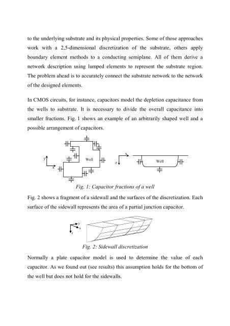
In CMOS circuits, <strong>for</strong> instance, capacitors model the depletion capacitance from<br />
the wells to substrate. It is necessary to divide the overall capacitance into<br />
smaller fractions. Fig. 1 shows an example of an arbitrarily shaped well and a<br />
possible arrangement of capacitors.<br />
y<br />
x<br />
Well<br />
z<br />
x<br />
Well<br />
Fig. 1: Capacitor fractions of a well<br />
Fig. 2 shows a fragment of a sidewall and the surfaces of the discretization. Each<br />
surface of the sidewall represents the area of a partial junction capacitor.<br />
z<br />
y<br />
x<br />
Fig. 2: Sidewall discretization<br />
Normally a plate capacitor model is used to determine the value of each<br />
capacitor. As we found out (see results) this assumption holds <strong>for</strong> the bottom of<br />
the well but does not hold <strong>for</strong> the sidewalls.