

ONFI Standards and What They Mean to Designers - Micron
ONFI Standards and What They Mean to Designers - Micron
ONFI Standards and What They Mean to Designers - Micron

Create successful ePaper yourself
Turn your PDF publications into a flip-book with our unique Google optimized e-Paper software.
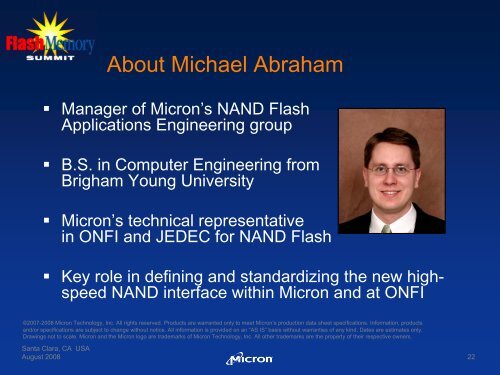
About Michael Abraham<br />
� Manager of <strong>Micron</strong>’s NAND Flash<br />
Applications Engineering group<br />
� B.S. in Computer Engineering from<br />
Brigham Young University<br />
� <strong>Micron</strong>’s technical representative<br />
in <strong>ONFI</strong> <strong>and</strong> JEDEC for NAND Flash<br />
� Key role in defining <strong>and</strong> st<strong>and</strong>ardizing the new highspeed<br />
NAND interface within <strong>Micron</strong> <strong>and</strong> at <strong>ONFI</strong><br />
©2007-2008 <strong>Micron</strong> Technology, Inc. All rights reserved. Products are warranted only <strong>to</strong> meet <strong>Micron</strong>’s production data sheet specifications. Information, products<br />
<strong>and</strong>/or specifications are subject <strong>to</strong> change without notice. All information is provided on an “AS IS” basis without warranties of any kind. Dates are estimates only.<br />
Drawings not <strong>to</strong> scale. <strong>Micron</strong> <strong>and</strong> the <strong>Micron</strong> logo are trademarks of <strong>Micron</strong> Technology, Inc. All other trademarks are the property of their respective owners.<br />
Santa Clara, CA USA<br />
August 2008 22


