

An Overview of SSD Write Caching (pdf) - Micron
An Overview of SSD Write Caching (pdf) - Micron
An Overview of SSD Write Caching (pdf) - Micron

Create successful ePaper yourself
Turn your PDF publications into a flip-book with our unique Google optimized e-Paper software.
<strong>An</strong> <strong>Overview</strong> <strong>of</strong> <strong>SSD</strong><br />
<strong>Write</strong> <strong>Caching</strong><br />
Doug Rollins, Senior Strategic Applications Engineer<br />
<strong>Micron</strong> Technology, Inc.<br />
Technical Marketing Brief<br />
What Is <strong>Write</strong> <strong>Caching</strong>, and Why Would<br />
I Enable It in My <strong>SSD</strong>?<br />
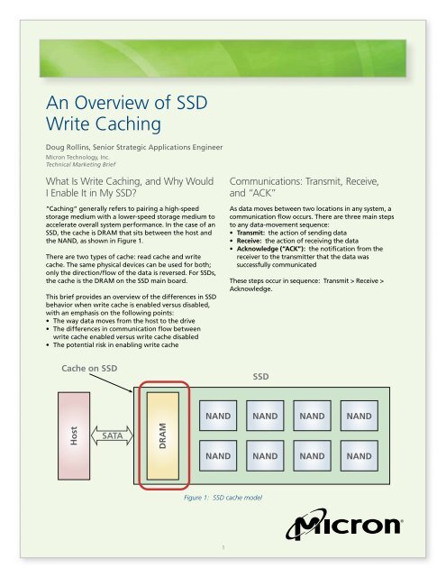
“<strong>Caching</strong>” generally refers to pairing a high-speed<br />
storage medium with a lower-speed storage medium to<br />
accelerate overall system performance. In the case <strong>of</strong> an<br />
<strong>SSD</strong>, the cache is DRAM that sits between the host and<br />
the NAND, as shown in Figure 1.<br />
There are two types <strong>of</strong> cache: read cache and write<br />
cache. The same physical devices can be used for both;<br />
only the direction/flow <strong>of</strong> the data is reversed. For <strong>SSD</strong>s,<br />
the cache is the DRAM on the <strong>SSD</strong> main board.<br />
This brief provides an overview <strong>of</strong> the differences in <strong>SSD</strong><br />
behavior when write cache is enabled versus disabled,<br />
with an emphasis on the following points:<br />
• The way data moves from the host to the drive<br />
• The differences in communication flow between<br />
write cache enabled versus write cache disabled<br />
• The potential risk in enabling write cache<br />
Cache on <strong>SSD</strong><br />
Host<br />
SATA<br />
DRAM<br />
NAND<br />
NAND<br />
Figure 1: <strong>SSD</strong> cache model<br />
1<br />
Communications: Transmit, Receive,<br />
and “ACK”<br />
As data moves between two locations in any system, a<br />
communication flow occurs. There are three main steps<br />
to any data-movement sequence:<br />
• Transmit: the action <strong>of</strong> sending data<br />
• Receive: the action <strong>of</strong> receiving the data<br />
• Acknowledge (“ACK”): the notification from the<br />
receiver to the transmitter that the data was<br />
successfully communicated<br />
These steps occur in sequence: Transmit > Receive ><br />
Acknowledge.<br />
<strong>SSD</strong><br />
NAND<br />
NAND<br />
NAND<br />
NAND<br />
NAND<br />
NAND
<strong>SSD</strong> Elements: Transmitters and<br />
Receivers<br />
For the scope <strong>of</strong> this document, we will assume that the<br />
transmitter is the host system and that the receiver is the<br />
<strong>SSD</strong>. This corresponds to a “write” command in which<br />
the host writes (transmits) data to the <strong>SSD</strong> (the receiver).<br />
The communications channel between the two is the<br />
host/drive interface. This can be SAS, SATA,<br />
FibreChannel, or any other drive interface.<br />
<strong>Write</strong> Traffic Flow: Cache Enabled<br />
When a host-to-<strong>SSD</strong> write occurs, data flows from the<br />
host, through the host:drive interface, to the <strong>SSD</strong>.<br />
<strong>Write</strong> cache enabled means that the <strong>SSD</strong> tells the host,<br />
“I have the data; please continue processing” as soon<br />
as the data reaches the DRAM buffer on the <strong>SSD</strong>. The<br />
data is moved from the DRAM buffer into the NAND<br />
opportunistically—that is, the <strong>SSD</strong> firmware controls<br />
this process and moves the data.<br />
2<br />
<strong>An</strong> <strong>Overview</strong> <strong>of</strong> <strong>SSD</strong> <strong>Write</strong> <strong>Caching</strong><br />
<strong>Write</strong> Traffic Flow: Cache Disabled<br />
When a host-to-<strong>SSD</strong> write occurs, data flows from the<br />
host, through the host/drive interface, to the <strong>SSD</strong>. This<br />
process is the same when write cache is enabled, but<br />
the sequence <strong>of</strong> communication is different.<br />
Potential Risk: Data Loss on Sudden<br />
Power Loss<br />
Although enabling write cache can substantially improve<br />
performance, it does increase the risk <strong>of</strong> data loss if the<br />
system power fails suddenly and unexpectedly.<br />
Why? Because when write cache is enabled, the drive<br />
“tells” the host that it “has the data” as soon as the<br />
data reaches the <strong>SSD</strong> DRAM buffer. The DRAM buffer<br />
is volatile (that is, it loses its contents when the power is<br />
removed). When the host receives the “ACK” message,<br />
the host assumes that the data is on the drive (and it is,<br />
but only on the drive’s DRAM) and will continue processing.<br />
If power is lost before the firmware moves the data<br />
from DRAM to NAND, the data is lost—but the host is<br />
completely unaware.<br />
Generally speaking, this is an acceptable risk in client<br />
systems. Enterprise systems, however, typically run with<br />
write cache disabled for the extra assurance that the data<br />
is more secure, that the host “knows” for certain when<br />
the data is in the NAND, and that the host knows how<br />
to handle sudden power losses (typically, by executing a<br />
write retry).
Steps Dialogue<br />
1 The host<br />
transmits data<br />
through the<br />
drive interface<br />
(SATA) to the<br />
<strong>SSD</strong>.<br />
2 The data<br />
moves from<br />
the host,<br />
through the<br />
drive interface,<br />
and into<br />
the DRAM<br />
buffer on the<br />
<strong>SSD</strong>.<br />
Note: Data<br />
always goes<br />
to the DRAM<br />
buffer on the<br />
<strong>SSD</strong> first—never<br />
straight to<br />
the NAND.<br />
3 The <strong>SSD</strong> then<br />
tells the host<br />
that it has a<br />
copy <strong>of</strong> the<br />
transmitted<br />
data and that<br />
the host is free<br />
to continue<br />
processing.<br />
Host to <strong>SSD</strong>:<br />
“…I’m sending<br />
you data;<br />
let me know<br />
when you<br />
have it…”<br />
<strong>SSD</strong> to host:<br />
“…OK, I have<br />
the data…”<br />
<strong>Write</strong> Traffic Flow: Cache Enabled<br />
DATA<br />
Host<br />
Host<br />
Host<br />
1: transmit<br />
SATA<br />
3<br />
DRAM<br />
<strong>An</strong> <strong>Overview</strong> <strong>of</strong> <strong>SSD</strong> <strong>Write</strong> <strong>Caching</strong><br />
NAND<br />
NAND<br />
NAND<br />
NAND<br />
NAND<br />
NAND<br />
Figure 2: The host transmits data to the <strong>SSD</strong>’s DRAM buffer.<br />
1: transmit<br />
DRAM<br />
NAND<br />
Figure 3: The data moves through the SATA interface and is received<br />
in the DRAM buffer.<br />
2: ACK<br />
DATA<br />
DRAM<br />
NAND<br />
NAND<br />
NAND<br />
NAND<br />
NAND<br />
NAND<br />
NAND<br />
NAND<br />
NAND<br />
NAND<br />
NAND<br />
Figure 4: The DRAM buffer immediately sends the host an<br />
acknowledgement <strong>of</strong> the data’s arrival.<br />
NAND<br />
NAND<br />
NAND<br />
NAND<br />
NAND<br />
NAND
Steps Dialogue<br />
4 Finally, the<br />
<strong>SSD</strong> automatically<br />
migrates<br />
the data from<br />
the DRAM<br />
buffer into the<br />
NAND (under<br />
the control<br />
<strong>of</strong> the <strong>SSD</strong><br />
firmware).<br />
Steps Dialogue<br />
1 The first step<br />
in the traffic<br />
flow when<br />
write cache is<br />
disabled is the<br />
same as when<br />
it is enabled:<br />
the host<br />
transmits data<br />
through the<br />
drive interface<br />
(SATA) to the<br />
<strong>SSD</strong>.<br />
2 The data<br />
moves from<br />
the host,<br />
through the<br />
drive interface,<br />
and into<br />
the DRAM<br />
buffer on the<br />
<strong>SSD</strong>.<br />
Note: Data<br />
always goes<br />
to the DRAM<br />
buffer on the<br />
<strong>SSD</strong> first—<br />
never straight<br />
to the NAND.<br />
Host to <strong>SSD</strong>:<br />
“…I’m sending<br />
you data;<br />
let me know<br />
when you<br />
have it…”<br />
Host<br />
Host<br />
Host<br />
1: transmit<br />
4<br />
DRAM<br />
<strong>An</strong> <strong>Overview</strong> <strong>of</strong> <strong>SSD</strong> <strong>Write</strong> <strong>Caching</strong><br />
NAND<br />
NAND<br />
NAND<br />
NAND<br />
NAND<br />
NAND<br />
Figure 6: The host transmits data to the <strong>SSD</strong>’s DRAM buffer.<br />
1: transmit<br />
DRAM<br />
<strong>Write</strong> Traffic Flow: Cache Disabled<br />
DATA<br />
DRAM<br />
3: Move<br />
(buffer to NAND)<br />
NAND<br />
NAND<br />
NAND<br />
NAND<br />
NAND<br />
NAND<br />
Figure 5: Instructed by the <strong>SSD</strong> firmware, the DRAM buffer<br />
opportunistically moves the data to the NAND.<br />
NAND<br />
NAND<br />
NAND<br />
NAND<br />
NAND<br />
NAND<br />
NAND<br />
NAND<br />
NAND<br />
NAND<br />
NAND<br />
NAND<br />
Figure 7: The data moves through the SATA interface and is received<br />
in the DRAM buffer.
Conclusion<br />
Steps Dialogue<br />
3 Next, the data<br />
is moved from<br />
the <strong>SSD</strong> DRAM<br />
buffer into the<br />
NAND.<br />
4 Only when<br />
the data has<br />
moved from<br />
the DRAM<br />
buffer to the<br />
NAND does<br />
the <strong>SSD</strong> inform<br />
the host that it<br />
“has the data”<br />
and that the<br />
host should<br />
continue processing.<br />
Enabling the write cache on any target adjusts how that<br />
target interacts with the host during data transmission<br />
and reception. With the cache enabled, the target<br />
acknowledges reception <strong>of</strong> data sooner, but because<br />
that data is stored (temporarily) in volatile DRAM, the<br />
data is potentially at risk due to sudden power loss.<br />
With the cache disabled, that acknowledgement does<br />
not occur until the data has been successfully programmed<br />
into the NAND.<br />
micron.com<br />
<strong>SSD</strong> to host:<br />
“…OK, I have<br />
the data…”<br />
Products are warranted only to meet <strong>Micron</strong>’s production data sheet<br />
specifications. Products and specifications are subject to change<br />
without notice.<br />
©2012 <strong>Micron</strong> Technology, Inc. <strong>Micron</strong>, the <strong>Micron</strong> logo, and Real<strong>SSD</strong> are trademarks <strong>of</strong> <strong>Micron</strong><br />
Technology, Inc. All other trademarks are the property <strong>of</strong> their respective owners. All rights<br />
reserved. 05/12 EN.L M:11841<br />
Host<br />
5<br />
DRAM<br />
<strong>An</strong> <strong>Overview</strong> <strong>of</strong> <strong>SSD</strong> <strong>Write</strong> <strong>Caching</strong><br />
NAND<br />
Figure 8: Instructed by the <strong>SSD</strong> firmware, the DRAM buffer opportunistically<br />
moves the data to the NAND.<br />
Host<br />
3: ACK<br />
DRAM<br />
2: Move<br />
(buffer to NAND)<br />
NAND<br />
NAND<br />
NAND<br />
NAND<br />
NAND<br />
NAND<br />
NAND<br />
NAND<br />
NAND<br />
NAND<br />
NAND<br />
NAND<br />
NAND<br />
NAND<br />
NAND<br />
Figure 9: The NAND sends the host an acknowledgement <strong>of</strong> the<br />
data’s arrival.<br />
While enabling the write cache on the <strong>SSD</strong> may improve<br />
performance in certain workloads, doing so requires an<br />
understanding <strong>of</strong> the resultant operations and the<br />
potential risks. For many hosts, the benefits far<br />
outweigh any associated risks (some <strong>of</strong> which can be<br />
mitigated by the use <strong>of</strong> an uninterruptable power<br />
supply [UPS]), while for others it does not. Because<br />
both the benefits and the potential risks are both<br />
platform- and workload-dependent, designers should<br />
give careful consideration to deciding whether to<br />
enable the write cache.


