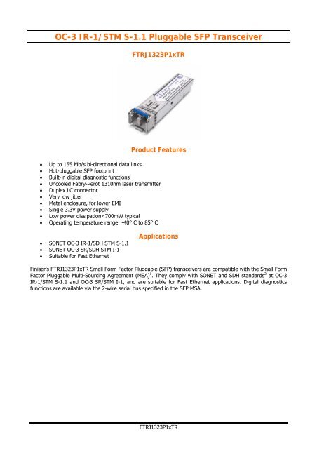
OC-3 IR-1/STM S-1.1 Pluggable SFP Transceiver
OC-3 IR-1/STM S-1.1 Pluggable SFP Transceiver
OC-3 IR-1/STM S-1.1 Pluggable SFP Transceiver

You also want an ePaper? Increase the reach of your titles
YUMPU automatically turns print PDFs into web optimized ePapers that Google loves.
<strong>OC</strong>-3 <strong>IR</strong>-1/<strong>STM</strong> S-<strong>1.1</strong> <strong>Pluggable</strong> <strong>SFP</strong> <strong>Transceiver</strong><br />
FTRJ1323P1xTR<br />
Product Features<br />
• Up to 155 Mb/s bi-directional data links<br />
• Hot-pluggable <strong>SFP</strong> footprint<br />
• Built-in digital diagnostic functions<br />
• Uncooled Fabry-Perot 1310nm laser transmitter<br />
• Duplex LC connector<br />
• Very low jitter<br />
• Metal enclosure, for lower EMI<br />
• Single 3.3V power supply<br />
• Low power dissipation
Pin Descriptions<br />
Pin Symbol Name/Description Ref.<br />
1 VEET Transmitter Ground (Common with Receiver Ground) 1<br />
2 TFAULT Transmitter Fault. Not supported.<br />
3 TDIS Transmitter Disable. Laser output disabled on high or open. 2<br />
4 MOD_DEF(2) Module Definition 2. Data line for Serial ID. 3<br />
5 MOD_DEF(1) Module Definition 1. Clock line for Serial ID. 3<br />
6 MOD_DEF(0) Module Definition 0. Grounded within the module. 3<br />
7 Rate Select No connection required 4<br />
8 LOS Loss of Signal indication. Logic 0 indicates normal operation. 5<br />
9 VEER Receiver Ground (Common with Transmitter Ground) 1<br />
10 VEER Receiver Ground (Common with Transmitter Ground) 1<br />
11 VEER Receiver Ground (Common with Transmitter Ground) 1<br />
12 RD- Receiver Inverted DATA out. AC Coupled<br />
13 RD+ Receiver Non-inverted DATA out. AC Coupled<br />
14 VEER Receiver Ground (Common with Transmitter Ground) 1<br />
15 VCCR Receiver Power Supply<br />
16 VCCT Transmitter Power Supply<br />
17 VEET Transmitter Ground (Common with Receiver Ground) 1<br />
18 TD+ Transmitter Non-Inverted DATA in. AC Coupled.<br />
19 TD- Transmitter Inverted DATA in. AC Coupled.<br />
20 VEET Transmitter Ground (Common with Receiver Ground) 1<br />
Notes:<br />
1. Circuit ground is internally isolated from chassis ground.<br />
2. Laser output disabled on TDIS>2.0V or open, enabled on TDIS
Absolute Maximum Ratings<br />
Parameter Symbol Min Typ Max Unit Ref.<br />
Maximum Supply Voltage VCC -0.5 4.7 V<br />
Storage Temperature TS -40 100 °C<br />
Case Operating Temperature TOP -40 85 °C<br />
Relative Humidity RH 0 85 % 1<br />
Electrical Characteristics (TOP = -40 to 85° C, VCC = 3.10 to 3.50 Volts)<br />
Parameter Symbol Min Typ Max Unit Ref.<br />
Supply Voltage VCC 3.10 3.50 V<br />
Supply Current ICC 165 300 mA<br />
Transmitter<br />
Input differential impedance Rin 100 Ω 2<br />
Single ended data input swing Vin,pp 250 1200 mV<br />
Transmit Disable Voltage VD VCC -1.3 VCC V<br />
Transmit Enable Voltage VEN Vee Vee+0.8 V 3<br />
Transmit Disable Assert Time 10 us<br />
Receiver<br />
Single ended data output swing Vout,pp 300 400 800 mV 4<br />
Data rise/fall time tr 250 500 ps 5<br />
LOS Fault VLOS fault VCC -0.5 VccHOST V 6<br />
LOS Normal VLOS norm Vee Vee+0.5 V 6<br />
Power Supply Rejection PSR 100 mVpp 7<br />
Notes:<br />
1. Non condensing.<br />
2. AC coupled.<br />
3. Or open circuit.<br />
4. Into 100 ohms differential termination.<br />
5. 20 – 80%<br />
6. Loss Of Signal is LVTTL. Logic 0 indicates normal operation; logic 1 indicates no signal detected.<br />
7. All transceiver specifications are compliant with a power supply sinusoidal modulation of 20 Hz to<br />
1.5 MHz up to specified value applied through the power supply filtering network shown on page<br />
23 of the Small Form-factor <strong>Pluggable</strong> (<strong>SFP</strong>) <strong>Transceiver</strong> MultiSource Agreement (MSA),<br />
September 14, 2000.<br />
FTRJ1323P1xTR
Optical Characteristics (TOP = -40 to 85° C, VCC = 3.10 to 3.50 Volts)<br />
Parameter Symbol Min Typ Max Unit Ref.<br />
Transmitter<br />
Output Opt. Pwr: 9/125 SMF POUT -15 -8 dBm 1<br />
Optical Wavelength ג 1261 1360 nm<br />
Spectral Width σ 7.7 nm<br />
Optical Extinction Ratio ER 8.2 dB<br />
Optical Rise/Fall Time tr/tf 500 ps 2<br />
Relative Intensity Noise RIN -120 dB/Hz<br />
Generated Jitter (peak to peak) JTXp-p 0.07 UI 3<br />
Generated Jitter (rms) JTXrms 0.007 UI 3<br />
Mask Margin 20%<br />
Receiver<br />
Average Rx Sensitivity @ <strong>OC</strong>-3 RSENS1 -28 -8 dBm 4<br />
Average Rx Sensitivity @ 125 Mb/s RSENS2 -28 -8 dBm 4<br />
Optical Center Wavelength גC 1260 1600 nm<br />
LOS De-Assert LOSD -28 dBm<br />
LOS Assert LOSA -45 dBm<br />
LOS Hysteresis 0.5 dB<br />
Notes:<br />
1. Class 1 Laser Safety per FDA/CDRH and EN (IEC) 60825 regulations.<br />
2. Unfiltered, 20-80%.<br />
3. Jitter measurements taken using Agilent OMNIBERT 718 in accordance with GR-253.<br />
4. With worst-case extinction ratio. Measured with a PRBS 2 23 -1 test pattern.<br />
General Specifications<br />
Parameter Symbol Min Typ Max Units Ref.<br />
Data Rate BR 125 155 Gb/sec 1<br />
Bit Error Rate BER 10 -12<br />
2<br />
Max. Supported Link Length on<br />
9/125µm SMF @ <strong>OC</strong>-3<br />
Notes:<br />
LMAX5 15 km 4<br />
1. Compliant with SONET and SDH at the following rates: <strong>OC</strong>-3 <strong>IR</strong>-1/<strong>STM</strong> S-<strong>1.1</strong> and <strong>OC</strong>-3 SR/<strong>STM</strong> I-1.<br />
2. Tested with a PRBS 2 23 -1 test pattern.<br />
3. Attenuation of 0.55 dB/km is used for the link length calculations (per GR-253 CORE). Distances are<br />
indicative only. Please refer to the Optical Specifications in Table IV to calculate a more accurate link<br />
budget based on specific conditions in your application.<br />
Environmental Specifications<br />
Finisar 1310nm <strong>SFP</strong> transceivers have an industrial operating temperature range from -40° C to +85° C case<br />
temperature.<br />
Parameter Symbol Min Typ Max Units Ref.<br />
Case Operating Temperature Top -40 85 °C<br />
Storage Temperature Tsto -40 100 °C<br />
Regulatory Compliance<br />
Finisar transceivers are Class 1 Laser Products and comply with US FDA regulations. These products are<br />
certified by TÜV and CSA to meet the Class 1 eye safety requirements of EN (IEC) 60825 and the electrical<br />
safety requirements of EN (IEC) 60950. Copies of certificates are available at Finisar Corporation upon<br />
request.<br />
FTRJ1323P1xTR
Digital Diagnostic Functions<br />
Finisar FTRJ1323P1xTR <strong>SFP</strong> transceivers support the 2-wire serial communication protocol as defined in the<br />
draft <strong>SFP</strong> MSA 1 . It is very closely related to the E 2 PROM defined in the GBIC standard, with the same<br />
electrical specifications.<br />
The standard <strong>SFP</strong> serial ID provides access to identification information that describes the transceiver’s<br />
capabilities, standard interfaces, manufacturer, and other information.<br />
Additionally, Finisar <strong>SFP</strong> transceivers provide a unique enhanced digital diagnostic monitoring interface,<br />
which allows real-time access to device operating parameters such as transceiver temperature, laser bias<br />
current, transmitted optical power, received optical power and transceiver supply voltage. It also defines a<br />
sophisticated system of alarm and warning flags, which alerts end-users when particular operating<br />
parameters are outside of a factory set normal range.<br />
The <strong>SFP</strong> MSA defines a 256-byte memory map in E 2 PROM that is accessible over a 2-wire serial interface at<br />
the 8 bit address 1010000X (A0h). The digital diagnostic monitoring interface makes use of the 8 bit address<br />
1010001X (A2h), so the originally defined serial ID memory map remains unchanged. The interface is<br />
identical to, and is thus fully backward compatible with both the GBIC Specification and the <strong>SFP</strong> Multi Source<br />
Agreement. The complete interface is described in Finisar Application Note AN-2030: “Digital Diagnostics<br />
Monitoring Interface for <strong>SFP</strong> Optical <strong>Transceiver</strong>s”.<br />
The operating and diagnostics information is monitored and reported by a Digital Diagnostics <strong>Transceiver</strong><br />
Controller (DDTC) inside the transceiver, which is accessed through a 2-wire serial interface. When the serial<br />
protocol is activated, the serial clock signal (SCL, Mod Def 1) is generated by the host. The positive edge<br />
clocks data into the <strong>SFP</strong> transceiver into those segments of the E 2 PROM that are not write-protected. The<br />
negative edge clocks data from the <strong>SFP</strong> transceiver. The serial data signal (SDA, Mod Def 2) is bi-directional<br />
for serial data transfer. The host uses SDA in conjunction with SCL to mark the start and end of serial<br />
protocol activation. The memories are organized as a series of 8-bit data words that can be addressed<br />
individually or sequentially.<br />
For more information, please see the <strong>SFP</strong> MSA documentation 1 or Finisar Application Note AN-2030.<br />
Digital diagnostics for the FTRJ1323P1xTR are externally calibrated by default.<br />
Please note that evaluation board FDB-1018 is available with Finisar ModDEMO software that allows simple<br />
to use communication over the 2-wire serial interface.<br />
FTRJ1323P1xTR
Mechanical Specifications<br />
Finisar’s Small Form Factor <strong>Pluggable</strong> (<strong>SFP</strong>) transceivers are compatible with the dimensions defined by the<br />
<strong>SFP</strong> Multi-Sourcing Agreement (MSA).<br />
FTRJ1323P1xTR
FTRJ1323P1xTR
References<br />
1. Small Form Factor <strong>Pluggable</strong> (<strong>SFP</strong>) <strong>Transceiver</strong> Multi-Source Agreement (MSA), September 2000.<br />
Documentation is currently available at Finisar upon request.<br />
2. Bellcore GR-253 and ITU-T G.957 Specifications.<br />
FTRJ1323P1xTR