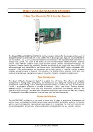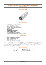
Multi-rate CWDM Pluggable SFP Transceiver
Multi-rate CWDM Pluggable SFP Transceiver
Multi-rate CWDM Pluggable SFP Transceiver

You also want an ePaper? Increase the reach of your titles
YUMPU automatically turns print PDFs into web optimized ePapers that Google loves.
<strong>Multi</strong>-<strong>rate</strong> <strong>CWDM</strong> <strong>Pluggable</strong> <strong>SFP</strong> <strong>Transceiver</strong><br />
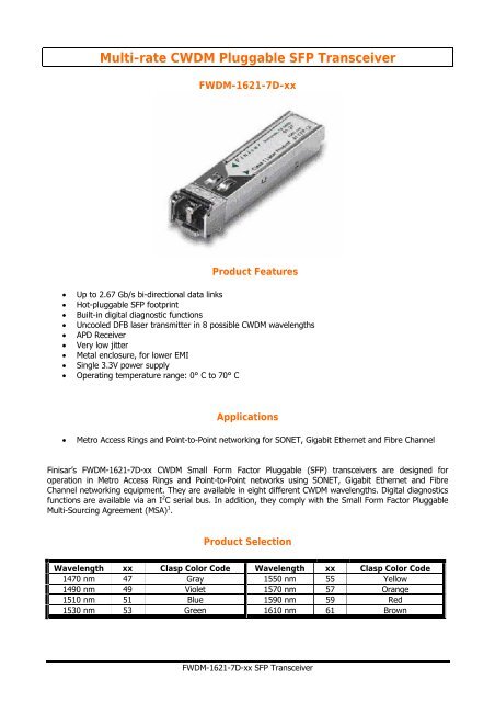
FWDM-1621-7D-xx<br />
Product Features<br />
• Up to 2.67 Gb/s bi-directional data links<br />
• Hot-pluggable <strong>SFP</strong> footprint<br />
• Built-in digital diagnostic functions<br />
• Uncooled DFB laser transmitter in 8 possible <strong>CWDM</strong> wavelengths<br />
• APD Receiver<br />
• Very low jitter<br />
• Metal enclosure, for lower EMI<br />
• Single 3.3V power supply<br />
• Operating temperature range: 0° C to 70° C<br />
Applications<br />
• Metro Access Rings and Point-to-Point networking for SONET, Gigabit Ethernet and Fibre Channel<br />
Finisar’s FWDM-1621-7D-xx <strong>CWDM</strong> Small Form Factor <strong>Pluggable</strong> (<strong>SFP</strong>) transceivers are designed for<br />
operation in Metro Access Rings and Point-to-Point networks using SONET, Gigabit Ethernet and Fibre<br />
Channel networking equipment. They are available in eight different <strong>CWDM</strong> wavelengths. Digital diagnostics<br />
functions are available via an I 2 C serial bus. In addition, they comply with the Small Form Factor <strong>Pluggable</strong><br />
<strong>Multi</strong>-Sourcing Agreement (MSA) 1 .<br />
Product Selection<br />
Wavelength xx Clasp Color Code Wavelength xx Clasp Color Code<br />
1470 nm 47 Gray 1550 nm 55 Yellow<br />
1490 nm 49 Violet 1570 nm 57 Orange<br />
1510 nm 51 Blue 1590 nm 59 Red<br />
1530 nm 53 Green 1610 nm 61 Brown<br />
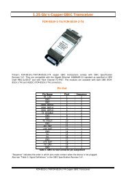
FWDM-1621-7D-xx <strong>SFP</strong> <strong>Transceiver</strong>
Pin Descriptions<br />
Pin Symbol Name/Description Ref.<br />
1 VEET Transmitter Ground (Common with Receiver Ground) 1<br />
2 TFAULT Transmitter Fault. Not supported.<br />
3 TDIS Transmitter Disable. Laser output disabled on high or open. 2<br />
4 MOD_DEF(2) Module Definition 2. Data line for Serial ID. 3<br />
5 MOD_DEF(1) Module Definition 1. Clock line for Serial ID. 3<br />
6 MOD_DEF(0) Module Definition 0. Grounded within the module. 3<br />
7 Rate Select No connection required 4<br />
8 LOS Loss of Signal indication. Logic 0 indicates normal operation. 5<br />
9 VEER Receiver Ground (Common with Transmitter Ground) 1<br />
10 VEER Receiver Ground (Common with Transmitter Ground) 1<br />
11 VEER Receiver Ground (Common with Transmitter Ground) 1<br />
12 RD- Receiver Inverted DATA out. AC Coupled<br />
13 RD+ Receiver Non-inverted DATA out. AC Coupled<br />
14 VEER Receiver Ground (Common with Transmitter Ground) 1<br />
15 VCCR Receiver Power Supply<br />
16 VCCT Transmitter Power Supply<br />
17 VEET Transmitter Ground (Common with Receiver Ground) 1<br />
18 TD+ Transmitter Non-Inverted DATA in. 100 ohm termination<br />
between TD+ and TD-, AC Coupled thereafter.<br />
19 TD- Transmitter Inverted DATA in. See TD+<br />
20 VEET Transmitter Ground (Common with Receiver Ground) 1<br />
Notes:<br />
1. Circuit ground is internally isolated from chassis ground.<br />
2. Laser output disabled on TDIS>2.0V or open, enabled on TDIS
Electrical Characteristics (TOP = 0 to 70° C, VCC = 3.15 to 3.60 Volts)<br />
Parameter Symbol Min Typ Max Unit Ref.<br />
Supply Voltage VCC 3.15 3.60 V<br />
Supply Current ICC 200 300 mA<br />
Transmitter<br />
Input differential impedance Rin 100 Ω 1<br />
Single ended data input swing Vin,pp 250 1200 mV<br />
Transmit Disable Voltage VD VCC -1.3 VCC V<br />
Transmit Enable Voltage VEN Vee Vee+0.8 V 2<br />
Transmit Disable Assert Time 10 us<br />
Receiver<br />
Single ended data output swing Vout,pp 250 800 mV 3<br />
Data output rise time tr 100 180 ps 4<br />
Data output fall time tf 100 180 ps 4<br />
LOS Fault VLOS fault VCC -0.5 VccHOST V 5<br />
LOS Normal VLOS norm Vee Vee+0.5 V 5<br />
Power Supply Rejection PSR 100 mVpp 6<br />
Notes:<br />
1. Connected directly to TX data input pins. AC coupled thereafter.<br />
2. Or open circuit.<br />
3. Into 100 ohms differential termination.<br />
4. 20 – 80%<br />
5. Loss Of Signal is LVTTL. Logic 0 indicates normal operation; logic 1 indicates no signal detected.<br />
6. Receiver sensitivity is compliant with power supply sinusoidal modulation of 20 Hz to 1.5 MHz up<br />
to specified value applied through the recommended power supply filtering network.<br />
Optical Characteristics (TOP = 0 to 70° C, VCC = 3.15 to 3.60 Volts)<br />
Parameter<br />
Transmitter<br />
Symbol Min Typ Max Unit Ref.<br />
Output Opt. Pwr: (End of Life) POUT +0 +5 dBm 1<br />
Optical Wavelength ג (x-4) (x+1) (x+7) nm 2<br />
Wavelength Temperature<br />
Dependance<br />
0.08 0.125 nm/°C<br />
Spectral Width (-20dB) σ 1 nm<br />
Optical Extinction Ratio ER 8.2 dB<br />
Sidemode Supression ratio SSRmin 30 dB<br />
Optical Rise/Fall Time tr/tf 180 ps 3<br />
Relative Intensity Noise RIN -120 dB/Hz<br />
Transmitter Jitter (peak to peak) 100 ps<br />
Receiver<br />
Average Rx Sensitivity @ 2.67 Gb/s RSENS1 -28 dBm 4<br />
Average Rx Sensitivity @ GbE RSENS1 -28 dBm 5<br />
Average Rx Sensitivity @ 2X FC RSENS1 -28 dBm 6<br />
Average Rx Sensitivity @ OC-12 RSENS1 -28 dBm 7<br />
Average Rx Sensitivity @ OC-3 RSENS1 -28 dBm 8<br />
Maximum Input Power PMAX -7 dBm<br />
Optical Center Wavelength גC 1270 1620 nm<br />
LOS De-Assert LOSD -32 dBm<br />
LOS Assert LOSA -42 dBm<br />
LOS Hysteresis 1.0 dB<br />
Receiver Jitter Generation<br />
@2.488Gbps<br />
130 ps 9<br />
Receiver Jitter Generation<br />
@1.25Gbps<br />
160 ps 10<br />
Dispersion Penalty at 100km 3 dB 11<br />
FWDM-1621-7D-xx <strong>SFP</strong> <strong>Transceiver</strong>
Notes:<br />
1. Class 1 Laser Safety per FDA/CDRH and IEC-825-1 regulations.<br />
2. Over case temperature of 0 to 70° C. The Transmitter Center Wavelength “x” is as specified by<br />
the customer. The current available wavelengths are: 1470, 1490, 1510, 1530, 1550, 1570, 1590,<br />
and 1610 nm. Please see the “Product Selection” section on page 1.<br />
3. Unfiltered.<br />
4. Worst-case extinction ratio. Measured with a PRBS 2 23 -1 test pattern.<br />
5. Worst-case extinction ratio. Measured with a PRBS 2 7 -1 test pattern.<br />
6. Worst-case extinction ratio. Measured with a PRBS 2 7 -1 test pattern.<br />
7. Worst-case extinction ratio. Measured with a PRBS 2 23 -1 test pattern.<br />
8. Worst-case extinction ratio. Measured with a PRBS 2 23 -1 test pattern.<br />
9. Jitter added by receiver (peak to peak). Measured at Average Rx Sensitivity of – 28dBm, PRBS 2 23<br />
-1 test pattern.<br />
10. Jitter added by receiver (peak to peak). Measured at Average Rx Sensitivity of – 28dBm, PRBS 2 7 -<br />
1 test pattern.<br />
11. Measured using 9/125µm SMF-28 @2.488Gbps, PRBS 2 23 -1 test pattern, BER
Digital Diagnostic Functions<br />
Finisar FWDM-1621-7D-xx <strong>SFP</strong> transceivers support the 2-wire serial communication protocol as defined in<br />
the draft <strong>SFP</strong> MSA 1 . It is very closely related to the E 2 PROM defined in the GBIC standard, with the same<br />
electrical specifications.<br />
The standard <strong>SFP</strong> serial ID provides access to identification information that describes the transceiver’s<br />
capabilities, standard interfaces, manufacturer, and other information.<br />
Additionally, Finisar <strong>SFP</strong> transceivers provide a unique enhanced digital diagnostic monitoring interface,<br />
which allows real-time access to device operating parameters such as transceiver temperature, laser bias<br />
current, transmitted optical power, received optical power and transceiver supply voltage. It also defines a<br />
sophisticated system of alarm and warning flags, which alerts end-users when particular operating<br />
parameters are outside of a factory set normal range.<br />
The <strong>SFP</strong> MSA defines a 256-byte memory map in E 2 PROM that is accessible over a 2-wire serial interface at<br />
the 8 bit address 1010000X (A0h). The digital diagnostic monitoring interface makes use of the 8 bit address<br />
1010001X (A2h), so the originally defined serial ID memory map remains unchanged. The interface is<br />
identical to, and is thus fully backward compatible with both the GBIC Specification and the <strong>SFP</strong> <strong>Multi</strong> Source<br />
Agreement. The complete interface is described in Finisar Application Note AN-2030: “Digital Diagnostics<br />
Monitoring Interface for <strong>SFP</strong> Optical <strong>Transceiver</strong>s”.<br />
Mechanical Specifications<br />
Finisar’s <strong>Multi</strong>-<strong>rate</strong> <strong>CWDM</strong> Small Form Factor <strong>Pluggable</strong> (<strong>SFP</strong>) transceivers are compatible with the<br />
dimensions defined by the <strong>SFP</strong> <strong>Multi</strong>-Sourcing Agreement (MSA).<br />
FWDM-1621-7D-xx (dimensions are in inches)<br />
FWDM-1621-7D-xx <strong>SFP</strong> <strong>Transceiver</strong>
FWDM-1621-7D-xx <strong>SFP</strong> <strong>Transceiver</strong>
(*) Neither IEEE 802.3 nor FC-PI 10.0 specifies a 1621 nm DFB single mode interface. The FWDM-1621-7Dxx<br />
complies with these specifications except for the following optical parameters, which have different<br />
values: transmitter wavelength, receiver sensitivity, and transmit output power. See Section IV for details.<br />
FWDM-1621-7D-xx <strong>SFP</strong> <strong>Transceiver</strong>