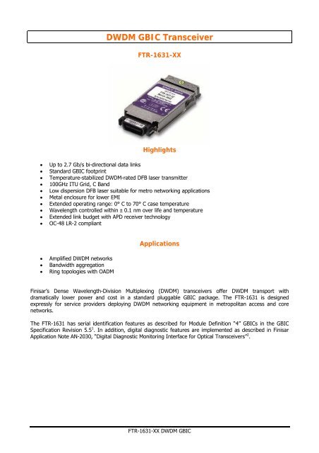
DWDM GBIC Transceiver
DWDM GBIC Transceiver
DWDM GBIC Transceiver

You also want an ePaper? Increase the reach of your titles
YUMPU automatically turns print PDFs into web optimized ePapers that Google loves.
<strong>DWDM</strong> <strong>GBIC</strong> <strong>Transceiver</strong><br />
FTR-1631-XX<br />
Highlights<br />
• Up to 2.7 Gb/s bi-directional data links<br />
• Standard <strong>GBIC</strong> footprint<br />
• Temperature-stabilized <strong>DWDM</strong>-rated DFB laser transmitter<br />
• 100GHz ITU Grid, C Band<br />
• Low dispersion DFB laser suitable for metro networking applications<br />
• Metal enclosure for lower EMI<br />
• Extended operating range: 0° C to 70° C case temperature<br />
• Wavelength controlled within ± 0.1 nm over life and temperature<br />
• Extended link budget with APD receiver technology<br />
• OC-48 LR-2 compliant<br />
• Amplified <strong>DWDM</strong> networks<br />
• Bandwidth aggregation<br />
• Ring topologies with OADM<br />
Applications<br />
Finisar’s Dense Wavelength-Division Multiplexing (<strong>DWDM</strong>) transceivers offer <strong>DWDM</strong> transport with<br />
dramatically lower power and cost in a standard pluggable <strong>GBIC</strong> package. The FTR-1631 is designed<br />
expressly for service providers deploying <strong>DWDM</strong> networking equipment in metropolitan access and core<br />
networks.<br />
The FTR-1631 has serial identification features as described for Module Definition “4” <strong>GBIC</strong>s in the <strong>GBIC</strong><br />
Specification Revision 5.5 1 . In addition, digital diagnostic features are implemented as described in Finisar<br />
Application Note AN-2030, “Digital Diagnostic Monitoring Interface for Optical <strong>Transceiver</strong>s” 2 .<br />
FTR-1631-XX <strong>DWDM</strong> <strong>GBIC</strong>
Product Selection<br />
Product Code Frequency (THz) Center Wavelength (nm)<br />
FTR-1631-17 191.7 1563.86<br />
FTR-1631-18 191.8 1563.05<br />
FTR-1631-19 191.9 1562.23<br />
FTR-1631-20 192.0 1561.42<br />
FTR-1631-21 192.1 1560.61<br />
FTR-1631-22 192.2 1559.79<br />
FTR-1631-23 192.3 1558.98<br />
FTR-1631-24 192.4 1558.17<br />
FTR-1631-25 192.5 1557.36<br />
FTR-1631-26 192.6 1556.55<br />
FTR-1631-27 192.7 1555.75<br />
FTR-1631-28 192.8 1554.94<br />
FTR-1631-29 192.9 1554.13<br />
FTR-1631-30 193.0 1553.33<br />
FTR-1631-31 193.1 1552.52<br />
FTR-1631-32 193.2 1551.72<br />
FTR-1631-33 193.3 1550.92<br />
FTR-1631-34 193.4 1550.12<br />
FTR-1631-35 193.5 1549.32<br />
FTR-1631-36 193.6 1548.51<br />
FTR-1631-37 193.7 1547.72<br />
FTR-1631-38 193.8 1546.92<br />
FTR-1631-39 193.9 1546.12<br />
FTR-1631-40 194.0 1545.32<br />
FTR-1631-41 194.1 1544.53<br />
FTR-1631-42 194.2 1543.73<br />
FTR-1631-43 194.3 1542.94<br />
FTR-1631-44 194.4 1542.14<br />
FTR-1631-45 194.5 1541.35<br />
FTR-1631-46 194.6 1540.56<br />
FTR-1631-47 194.7 1539.77<br />
FTR-1631-48 194.8 1538.98<br />
FTR-1631-49 194.9 1538.19<br />
FTR-1631-50 195.0 1537.40<br />
FTR-1631-51 195.1 1536.61<br />
FTR-1631-52 195.2 1535.82<br />
FTR-1631-53 195.3 1535.04<br />
FTR-1631-54 195.4 1534.25<br />
FTR-1631-55 195.5 1533.47<br />
FTR-1631-56 195.6 1532.68<br />
FTR-1631-57 195.7 1531.90<br />
FTR-1631-58 195.8 1531.12<br />
FTR-1631- 59 195.9 1530.33<br />
FTR-1631-60 196.0 1529.55<br />
FTR-1631-61 196.1 1528.77<br />
FTR-1631-XX <strong>DWDM</strong> <strong>GBIC</strong>
Pin Out<br />
Pin Name Pin# Sequence<br />
RX_LOS 1 2<br />
GND 2 2<br />
GND 3 2<br />
MOD_DEF(0) 4 2<br />
MOD_DEF(1) 5 2<br />
MOD_DEF(2) 6 2<br />
TX_DISABLE 7 2<br />
GND 8 2<br />
GND 9 2<br />
TX_FAULT 10 2<br />
GND 11 1<br />
-RX_DAT 12 1<br />
+RX_DAT 13 1<br />
GND 14 1<br />
Vcc 15 2<br />
Vcc 16 2<br />
GND 17 1<br />
+TX_DAT 18 1<br />
-TX_DAT 19 1<br />
GND 20 1<br />
Table 1. <strong>GBIC</strong> to Host Connector Pin Assignment<br />
“Sequence” indicates the order in which pins make contact when the device is hot plugged.<br />
Also see “Table 3: Signal Definitions” in the <strong>GBIC</strong> Specification Revision 5.5 1 for a description of the<br />
function of each pin listed above.<br />
Electrical Power Interface<br />
The <strong>GBIC</strong> specification calls for a range of 4.75V to 5.25 volts as described in Table 2. The maximum<br />
voltage of 6V is not to be continuously.<br />
Parameter Symbol Min Typ Max Units Notes/Conditions<br />
Supply Current Is 250 400 mA<br />
Inrush Current Isurge 30 mA<br />
=300 msec above<br />
steady state current<br />
Maximum<br />
Voltage<br />
Vmax 6 V<br />
Input Voltage Vcc 4.75 5.0 5.25 V Referenced to GND.<br />
Table 2. Electrical Power Interface<br />
Low Speed Signals<br />
RX_LOS, TX_DISABLE, and TX_FAULT are TTL signals as described in Table 3. MOD_DEF(1) (SCL) and<br />
MOD_DEF(2) (SDA), are open drain CMOS signals (see section IX, “Serial Communication Protocol”). Both<br />
MOD_DEF(1) and MOD_DEF(2) must be pulled up to host_Vcc. For more information, see sections 5.3.1 –<br />
5.3.8 in the <strong>GBIC</strong> Specification Revision 5.5 1 .<br />
For more detailed information, see sections 5.3.1 – 5.3.8 in the <strong>GBIC</strong> Specification Rev. 5.4 1 .<br />
Parameter Symbol Min Max Units Notes/Conditions<br />
<strong>GBIC</strong> Output<br />
LOW<br />
VOL 0 0.5 V<br />
FTR-1631-XX <strong>DWDM</strong> <strong>GBIC</strong><br />
4.7k to 10k pull-up to<br />
host_VCC, measured at host
<strong>GBIC</strong> Output<br />
HIGH<br />
<strong>GBIC</strong> Input<br />
LOW<br />
<strong>GBIC</strong> Input<br />
HIGH<br />
VOH<br />
Host_VCC<br />
-0.5<br />
Host_VCC<br />
+0.3<br />
VIL 0 0.8 V<br />
FTR-1631-XX <strong>DWDM</strong> <strong>GBIC</strong><br />
V<br />
side of connector<br />
4.7k to 10k pull-up to<br />
host_VCC, measured at host<br />
side of connector<br />
4.7k to 10k pull-up to VCC,<br />
measured at <strong>GBIC</strong> side of<br />
connector<br />
VIH 2 VCC + 0.3 V<br />
4.7k to 10k pull-up to VCC,<br />
measured at <strong>GBIC</strong> side of<br />
connector<br />
Table 3. Low Speed Signals – Electronic Characteristics<br />
Parameter Symbol Min Typ Max Units Notes/Conditions<br />
RX_LOS Assert<br />
Level<br />
-42 -36 dBm<br />
RX_LOS Deassert<br />
Level<br />
-34 -32 dBm<br />
RX_LOS<br />
Hysteresis<br />
2 dB<br />
RX_LOS Assert<br />
Delay<br />
t_loss_on 300 µsec<br />
From detection of loss<br />
of signal to assertion<br />
of RX_LOS<br />
RX_LOS Negate<br />
Delay<br />
t_loss_off 150 µsec<br />
From detection of<br />
presence of signal to<br />
negation of RX_LOS<br />
Rising edge of<br />
TX_DISABLE<br />
Assert Time<br />
t_off 1.5 msec<br />
TX_DISABLE to fall of<br />
output signal below<br />
10% of nominal<br />
Falling edge of<br />
TX_DISABLE to rise of<br />
output signal above<br />
TX_DISABLE<br />
Negate Time<br />
t_on 6.0 msec<br />
90% of nominal. Time<br />
indicated is under<br />
steady-state<br />
temperature<br />
conditions.<br />
TX_DISABLE<br />
Reset Time<br />
t_reset 10 µsec<br />
TX_DISABLE HIGH<br />
before TX_DISABLE<br />
set LOW<br />
TX_Fault will assert<br />
TX_FAULT Assert -0.1 0.1 nm<br />
before the device is<br />
outside of specified<br />
wavelength range<br />
Table 4. Low Speed Signal Parameters
High Speed Electrical Interface<br />
All high-speed PECL signals are AC coupled internally.<br />
Parameter Symbol Min Typ Max Units Notes/Conditions<br />
Data Input<br />
Voltage<br />
Vin 650 2000 mV<br />
PECL differential<br />
peak-peak<br />
Data Output<br />
Voltage<br />
Vout 370 2000 mV<br />
PECL differential<br />
peak-peak<br />
PECL rise/fall Tr, Tf 150 psec 20%-80% Differential<br />
Bit Error Rate BER 10 -12<br />
PRBS 2 23 – 1 test data<br />
pattern<br />
Tx Input<br />
Impedance<br />
Zin 75 ohm<br />
Rx Output<br />
Impedance<br />
Zout 75 ohm<br />
Table 5. High-Speed Electrical Interface<br />
Optical Parameters<br />
Parameter Symbol Min Typ Max Units Notes/Conditions<br />
Transmitter Characteristics<br />
Center<br />
Wavelength<br />
Spacing<br />
Spectral<br />
Width<br />
Transmitter<br />
Center<br />
Wavelengt -<br />
End of Life<br />
Transmitter<br />
Center<br />
Wavelength -<br />
Start of Life<br />
Side Mode<br />
Suppression<br />
Ratio (SMSR)<br />
Optical<br />
Rise/Fall<br />
Time<br />
Transmitter<br />
Optical<br />
Output Power<br />
Transmitter<br />
Extinction<br />
Ratio<br />
Transmitter<br />
Eye Opening<br />
Transmitter<br />
Jitter<br />
Receiver Characteristics<br />
Optical Input<br />
Wavelength<br />
Receiver<br />
Jitter<br />
100 GHz<br />
∆λ20 0.2 0.3 nm<br />
λC X-100 X X+100 pm<br />
λC X-80 V-50 X-20 pm<br />
FTR-1631-XX <strong>DWDM</strong> <strong>GBIC</strong><br />
Corresponds to<br />
approximately 0.8 nm<br />
Full width, -20dB from<br />
max<br />
X = specified center<br />
wavelength<br />
X = specified center<br />
wavelength<br />
SMSR 30 dB Modulated<br />
tr/tf 160 ps Unfiltered, 80%-20%<br />
Pout 0 +4 dBm<br />
OMI 8.2 dB<br />
Pin<br />
10 %<br />
75 mUI<br />
1520 1570 nm<br />
75 mUI<br />
Average power<br />
coupled into single<br />
mode fiber<br />
OC-48 eye mask<br />
margin<br />
Parameters per GR-<br />
253 4 section 5.6 for<br />
OC-48 B<br />
Parameters per GR-<br />
253 4 section 5.6 for
Generation OC-48 B<br />
Optical Input<br />
Power<br />
(BER
Storage Temp Tsto -10 85 °C<br />
of device<br />
Ambient temperature<br />
CDRH and IEC-825<br />
Eye Sefety<br />
Class 1 Laser<br />
Product. See Note 1<br />
Note 1: Complies with FDA performance standards for laser products except for deviations pursuant to Laser Notice No.<br />
50, dated July 26, 2001.<br />
Table 8. Environmental Specifications<br />
Serial Communication Protocol<br />
All Finisar optical <strong>GBIC</strong>s implement serial identification features described for ‘Module Definition “4”’ as<br />
outlined in Annex D of the <strong>GBIC</strong> Specification 1 . These <strong>GBIC</strong>s use an Atmel AT24C01A 128 byte E 2 PROM at<br />
address A0H. For details on interfacing with the E 2 PROM, see the Atmel data sheet titled<br />
“AT24C01A/02/04/08/16 2-Wire Serial CMOS E 2 PROM”. 3<br />
Finisar’s <strong>DWDM</strong> <strong>GBIC</strong>s also support extended diagnostic features as described in Finisar Applications Note<br />
AN-2030, “Digital Diagnostic Monitoring Interface for Optical <strong>Transceiver</strong>s” 2 . A controller IC that monitors<br />
system parameters such as laser current, module temperature, transmitter power, and received power is<br />
accessible at address A2H.<br />
Parameter Symbol Min Typ Max Units Notes/Conditions<br />
I 2 C Clock for<br />
Atmel (A0H)<br />
and Controller<br />
IC (A2H)<br />
Catmel 0 100,000 Hz<br />
Table 9. I 2 C Timing Requirements<br />
FTR-1631-XX <strong>DWDM</strong> <strong>GBIC</strong><br />
Bus can be driven<br />
blind.
Mechanical Specifications<br />
Finisar’s <strong>DWDM</strong> <strong>GBIC</strong>s conform to the mechanical specifications outlined in the <strong>GBIC</strong> Specification Revision<br />
5.5, Section 6 1 .<br />
Parameter Symbol Min Typ Max Units Notes/Conditions<br />
<strong>GBIC</strong> insertion F1 0 20 Newtons ~4.5 lbs<br />
<strong>GBIC</strong> extraction FE 0 15 Newtons ~3.3 lbs<br />
<strong>GBIC</strong> retention FR 130 Newtons Straight out ~29.3 lbs<br />
Table 10. Insertion, Extraction, and Retention Forces<br />
Ordering Information<br />
Part Number Description<br />
FTR-1631-XX <strong>DWDM</strong> <strong>GBIC</strong> with APD Receiver<br />
XX = channel number (see product selection on page 2)<br />
References<br />
1. “Gigabit Interface Converter (<strong>GBIC</strong>) Revision 5.5”. Sun Microsystems Computer Company et. al.,<br />
August 16, 1999. http://playground.sun.com/pub/OEmod/<br />
2. “Application Note AN-2030: Digital Diagnostic Monitoring Interface for SFP Optical <strong>Transceiver</strong>s”,<br />
Finisar Corporation, April 2002.<br />
3. “AT24C01A/02/04/08/16 2-Wire Serial CMOS E 2 PROM”. Atmel Corporation. www.Atmel.com.<br />
4. “SONET Transport Systems: Common Generic Criteria”, Telcordia Technologies, GR-253-CORE, Issue<br />
3, September 2000.<br />
FTR-1631-XX <strong>DWDM</strong> <strong>GBIC</strong>