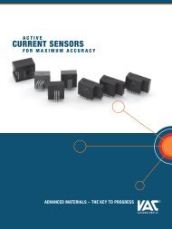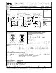
4646-X413 - Vacuumschmelze
4646-X413 - Vacuumschmelze
4646-X413 - Vacuumschmelze

Create successful ePaper yourself
Turn your PDF publications into a flip-book with our unique Google optimized e-Paper software.
VACUUMSCHMELZE<br />
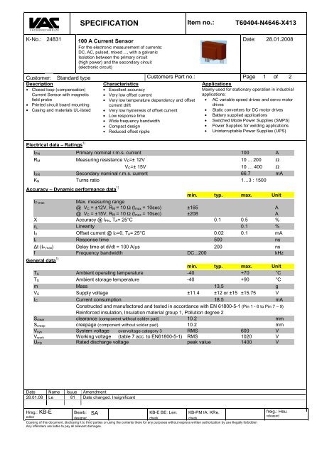
SPECIFICATION Item no.: T60404-N<strong>4646</strong>-<strong>X413</strong><br />
K-No.: 24831 100 A Current Sensor Date: 28.01.2008<br />
For the electronic measurement of currents:<br />
DC, AC, pulsed, mixed ..., with a galvanic<br />
Isolation between the primary circuit<br />
(high power) and the secondary circuit<br />
(electronic circuit)<br />
Customer: Standard type Customers Part no.: Page 1 of 2<br />
Description<br />
• Closed loop (compensation)<br />
Current Sensor with magnetic<br />
field probe<br />
• Printed circuit board mounting<br />
• Casing and materials UL-listed<br />
Electrical data – Ratings 1)<br />
Characteristics<br />
• Excellent accuracy<br />
• Very low offset current<br />
• Very low temperature dependency and offset<br />
current drift<br />
• Very low hysteresis of offset current<br />
• Low response time<br />
• Wide frequency bandwidth<br />
• Compact design<br />
• Reduced offset ripple<br />
Applications<br />
Mainly used for stationary operation in industrial<br />
applications:<br />
• AC variable speed drives and servo motor<br />
drives<br />
• Static converters for DC motor drives<br />
• Battery supplied applications<br />
• Switched Mode Power Supplies (SMPS)<br />
• Power Supplies for welding applications<br />
• Uninterruptable Power Supplies (UPS)<br />
I PN Primary nominal r.m.s. current 100 A<br />
R M Measuring resistance V C=± 12V 10 ... 200 Ω<br />
V C=± 15V 10 … 400 Ω<br />
I SN Secondary nominal r.m.s. current 66.7 mA<br />
K N Turns ratio 1…3 : 1500<br />
min. typ. max. Unit<br />
I P,max<br />
Max. measuring range<br />
@ V C = ±12V, R M = 10 Ω (t max = 10sec) ±165 A<br />
@ V C = ±15V, R M = 10 Ω (t max = 10sec) ±208 A<br />
X Accuracy @ I PN, T A= 25°C 0.1 0.5 %<br />
ε L Linearity 0.1 %<br />
I 0 Offset current @ I P=0, T A= 25°C 0.02 0.1 mA<br />
t r Response time 500 ns<br />
Δt (I P,max) Delay time at di/dt = 100 A/µs 200 ns<br />
f Frequency bandwidth DC...200 kHz<br />
min. typ. max. Unit<br />
T A Ambient operating temperature -40 +70 °C<br />
T S Ambient storage temperature -40 +90 °C<br />
m Mass 13,5 g<br />
V C Supply voltage ±11.4 ±12 or ±15 ±15.75 V<br />
I C Current consumption 18.5 mA<br />
Constructed and manufactored and tested in accordance with EN 61800-5-1 (Pin 1 - 6 to Pin 7 – 9)<br />
Reinforced insulation, Insulation material group 1, Pollution degree 2<br />
S clear clearance (component without solder pad) 10.2 mm<br />
S creep creepage (component without solder pad) 10.2 mm<br />
V sys System voltage overvoltage category 3 RMS 600 V<br />
V work Working voltage (table 7 acc. to EN61800-5-1) RMS 1020 V<br />
U PD Rated discharge voltage peak value 1400 V<br />
Date Name Isuue Amendment<br />
28.01.08 Le 81 Date changed. Insignificant<br />
Hrsg.: KB-E<br />
Bearb: SA<br />
KB-E BE: Len. KB-PM IA: KRe.<br />
editor<br />
designer check<br />
check<br />
Copying of this document, disclosing it to third parties or using the contents there for any purposes without express written authorization by use illegally forbidden<br />
Any offenders are liable to pay all relevant damages.<br />
freig.: Heu.<br />
released
VACUUMSCHMELZE<br />
SPECIFICATION Item no.: T60404-N<strong>4646</strong>-<strong>X413</strong><br />
K-No.: 24831 100 A Current Sensor Date: 28.01.2008<br />
For the electronic measurement of currents:<br />
DC, AC, pulsed, mixed ..., with a galvanic<br />
Isolation between the primary circuit<br />
(high power) and the secondary circuit<br />
(electronic circuit)<br />
Customer: Standard type Customers Part no.: Page 2 of 2<br />
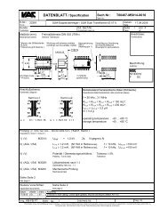
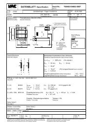
Mechanical outline (mm): General tolerances DIN ISO 2768-c<br />
1,74<br />
1,905<br />
7 9<br />
33,25<br />
Z<br />
4 6<br />
Toleranz der Stiftabstände<br />
±0,2mm<br />
Einzelheit<br />
Z<br />
0,6<br />
Connections:<br />
1...6: ∅ 1,5 mm<br />
7...9: 0,6x0,7 mm<br />
11,43<br />
1,29<br />
(2,64)<br />
F<br />
DC<br />
12,7<br />
3<br />
1<br />
2x2,54<br />
7,75<br />
7,6<br />
0,7<br />
14,45<br />
Marking:<br />
<strong>4646</strong><strong>X413</strong><br />
F DC<br />
21<br />
3,5±0.5<br />
0,65<br />
3x 0,7x0,6 6x Ø1,5<br />
DC = Date Code<br />
F= Factory<br />
Schematic diagram<br />
1...3<br />
Ip<br />
+<br />
8 + V C<br />
7 I S<br />
+<br />
+<br />
-<br />
R M<br />
C A<br />
4...6<br />
9 - V C<br />
M<br />
Possibilities of wiring for V C = ±15V (@ T A = 70°C, R M = 15 Ω)<br />
primary primary current output current turns ratio primary wiring<br />
windings RMS maximal RMS resistance<br />
N P I P [A] Î P,max [A] I S (I P) [mA] K N R P [mW]<br />
. .<br />
1 100 208 66.7 1:1500 0.12 > 1 3<br />
.<br />
. 6 4 > .<br />
> 1 3<br />
2 35 104 46.7 2:1500 0.54<br />
6 4 ><br />
. .<br />
3 25 69 50 3:1500 1.1 > 1 3<br />
.<br />
. 6 4 > .<br />
Temperature of the primary conductor should not exceed 100°C.<br />
Additional information is obtainable on request.<br />
This specification is no declaration of warranty acc. BGB §443 dar.<br />
Hrsg.: KB-E<br />
Bearb: SA<br />
KB-E BE: Len. KB-PM IA: KRe.<br />
editor<br />
designer check<br />
check<br />
Copying of this document, disclosing it to third parties or using the contents there for any purposes without express written authorization by use illegally forbidden<br />
Any offenders are liable to pay all relevant damages.<br />
freig.: Heu.<br />
released
Additional Information Item No.: T60404-N<strong>4646</strong>-<strong>X413</strong><br />
VACUUMSCHMELZE<br />
K-No.: 24831<br />
100 A Current Sensor<br />
For electronic current measurement:<br />
DC, AC, pulsed, mixed ..., with a galvanic<br />
isolation between primary circuit<br />
(high power) and secondary circuit<br />
Date: 28.01.2008<br />
Customer: Customers Part No.: Page 1 of 3<br />
ME<br />
A=km<br />
1=St<br />
2=kg<br />
3=g<br />
4=l<br />
5=m<br />
6=m²<br />
7=m³<br />
8=mm<br />
9:Paar<br />
min. typ. max. Unit<br />
V Ctot Maximum supply voltage (without function) ±18 V<br />
±15.75 … ±18 V: for 1s per hour<br />
R S Secondary coil resistance @ T A=70°C 88 Ω<br />
R p Primary coil resistance per turn @ T A=25°C 0.36 mΩ<br />
X Ti Temperature drift of X @ T A = -40 ... +70 °C 0.1 %<br />
I 0ges Offset current (including I 0, I 0t, I 0T) 0.12 mA<br />
I 0t Long term drift Offset current I 0 0.04 mA<br />
I 0T Offset current temperature drift I 0 @ T A = -40 ...+70°C 0.04 mA<br />
I 0H Hyteresis current @ I P=0 (caused by primary current 3 x I PN) 0.03 0.07 mA<br />
∆I 0/∆V C Supply voltage rejection ratio 0.01 mA/V<br />
i oss Offset ripple* (with1 MHz- filter first order) 0.15 mA<br />
i oss Offset ripple* (with 100 kHz- filter first order) 0.035 0.05 mA<br />
i oss Offset ripple* (with 20 kHz- filter first order) 0.009 0.012 mA<br />
C k Maximum possible coupling capacity (primary – secondary) 5 pF<br />
Mechanical Stress according to M3209/3<br />
10g<br />
Settings: 10 – 2000 Hz, 1 min/Decade, 2 hours<br />
An exceptionally high rate of on/off – switching of the supply voltage<br />
accelerates the aging process of the sensor.<br />
Inspection 1)<br />
(Measurement after temperature balance of the samples at room temperature)<br />
K N(N 1/N 2) (V) M3011/6 Transformation ratio (I P=3*10A, 40-80 Hz) 1…3 : 1500 ± 0.5 %<br />
I 0 (V) M3226 Offset current < 0.07 mA<br />
V P,eff (V) M3014 Test voltage, rms, 1s 2.5 kV<br />
Pin 1 - 6 to Pin 7 - 9<br />
V e (AQL 1/S4) Partial discharge voltage acc. M3024 (RMS) 1500 V<br />
with V vor (RMS) 1875 V<br />
Type Testing (Pin 1 - 6 to Pin 7 – 9)<br />
Designed according standard EN 61800 with insulation material group 1<br />
V W HV transient test according (to M3064) 8 kV<br />
(1,2 µs / 50 µs-wave form)<br />
V d Testing voltage acc. M3014 (RMS) (5 s) 5 kV<br />
V e Partial discharge voltage acc. M3024 (RMS) 1500 V<br />
with V vor (RMS) 1875 V<br />
Datum Name Index Änderung<br />
28.01.08 Le 81 Page 3: write error in X ges (I PN). changed. Insignificant<br />
Hrsg.: KB-E<br />
Bearb: SA<br />
editor<br />
designer check<br />
Weitergabe sowie Vervielfältigung dieser Unterlage, Verwertung und Mitteilung ihres Inhalts<br />
nicht gestattet, soweit nicht ausdrücklich zugestanden. Zuwiderhandlungen verpflichten zu<br />
Schadenersatz. Alle Rechte für den Fall der Patenterteilung oder GM-Eintragung vorbehalten<br />
KB-E BE: Len<br />
KB-PM IA: KRe.<br />
freig.: Heu.<br />
released<br />
check<br />
Copying of this document, disclosing it to third parties or using the contents there for any<br />
purposes without express written authorization by use illegally forbidden.<br />
Any offenders are liable to pay all relevant damages.
Additional Information Item No.: T60404-N<strong>4646</strong>-<strong>X413</strong><br />
VACUUMSCHMELZE<br />
K-No.: 24831<br />
100 A Current Sensor<br />
For electronic current measurement:<br />
DC, AC, pulsed, mixed ..., with a galvanic<br />
isolation between primary circuit<br />
(high power) and secondary circuit<br />
Date: 28.01.2008<br />
Customer: Customers Part No.: Page 2 of 3<br />
ME<br />
A=km<br />
1=St<br />
2=kg<br />
3=g<br />
4=l<br />
5=m<br />
6=m²<br />
7=m³<br />
8=mm<br />
9:Paar<br />
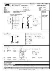
Limit curve of measurable current Î P(R M)<br />
@ ambient temperature T A ≤ 85 °C<br />
N P<br />
* Î P<br />
[A]<br />
250<br />
200<br />
150<br />
100<br />
50<br />
0<br />
V C<br />
= +/-12V - 5%<br />
V C<br />
= +/-15V - 5%<br />
0 20 40 60 80 100 120 140 160 180 200 220 240<br />
R M<br />
[Ω]<br />
1)<br />
Maximum measuring range (µs-range) 1)<br />
Output current behaviour of a 3kA current pulse<br />
@ V C = ±15V und R M= 25Ω<br />
I [A]<br />
1000<br />
800<br />
600<br />
400<br />
200<br />
0<br />
-200<br />
Ip [A]<br />
Ia / KN [A]<br />
0 1 2 3<br />
t [µs]<br />
Fast increasing currents (higher than the specified I p,max), e.g. in case<br />
of a short circuit, can be transmitted because the currents are<br />
transformed directly.<br />
The offset ripple can be reduced by an external low pass. Simplest solution is a passive low pass filter of 1st order with<br />
f<br />
g<br />
1<br />
= 2π<br />
⋅ R<br />
M<br />
⋅C<br />
a<br />
In this case the response time is enlarged.<br />
It is calculated from:<br />
t′<br />
≤ t + 2, 5R<br />
r<br />
r<br />
M<br />
C<br />
a<br />
Applicable documents<br />
Current direction: A positive output current appears at point I S, by primary current in direction of the arrow.<br />
Constructed and manufactored and tested in accordance with EN 61800.<br />
Housing and bobbin material UL-listed: Flammability class 94V-0.<br />
Hrsg.: KB-E<br />
Bearb: SA<br />
editor<br />
designer check<br />
Weitergabe sowie Vervielfältigung dieser Unterlage, Verwertung und Mitteilung ihres Inhalts<br />
nicht gestattet, soweit nicht ausdrücklich zugestanden. Zuwiderhandlungen verpflichten zu<br />
Schadenersatz. Alle Rechte für den Fall der Patenterteilung oder GM-Eintragung vorbehalten<br />
KB-E BE: Len<br />
KB-PM IA: KRe.<br />
freig.: Heu.<br />
released<br />
check<br />
Copying of this document, disclosing it to third parties or using the contents there for any<br />
purposes without express written authorization by use illegally forbidden.<br />
Any offenders are liable to pay all relevant damages.
Additional Information Item No.: T60404-N<strong>4646</strong>-<strong>X413</strong><br />
VACUUMSCHMELZE<br />
K-No.: 24831<br />
100 A Current Sensor<br />
For electronic current measurement:<br />
DC, AC, pulsed, mixed ..., with a galvanic<br />
isolation between primary circuit<br />
(high power) and secondary circuit<br />
Date: 28.01.2008<br />
Customer: Customers Part No.: Page 3 of 3<br />
ME<br />
A=km<br />
1=St<br />
2=kg<br />
3=g<br />
4=l<br />
5=m<br />
6=m²<br />
7=m³<br />
8=mm<br />
9:Paar<br />
I 0H:<br />
I 0t:<br />
t r:<br />
∆t (I Pmax):<br />
X ges(I PN):<br />
Zero variation of I o after overloading with a DC of tenfold the rated value (R M = R MN)<br />
Long term drift of I o after 100 temperature cycles in the range -40 bis 85 °C.<br />
Response time (describe the dynamic performance for the specified measurement range), measured as delay time<br />
at I P = 0,9 . I Pmax between a rectangular current and the output current.<br />
Delay time (describe the dynamic performance for the rapid current pulse rate e.g short circuit current)<br />
measured between I Pmax and the output current i a with a primary current rise of di 1/dt = 100 A/µs.<br />
The sum of all possible errors over the temperature range by measuring a current I PN:<br />
IS<br />
( IPN<br />
)<br />
X<br />
ges = 100 ⋅ − 1 %<br />
K ⋅ I<br />
N<br />
PN<br />
X: Permissible measurement error in the final inspection at RT, defined by<br />
X<br />
I<br />
= 100 ⋅<br />
SB − 1 %<br />
I<br />
SN<br />
where I SB is the output DC value of an input DC current of the same magnitude as the (positive) rated current (I o = 0 )<br />
X Ti:<br />
ε L:<br />
Temperature drift of the rated value orientated output term. I SN (cf. Notes on F i) in a specified temperature range,<br />
obtained by:<br />
I<br />
( T ) − I ( T )<br />
SB A2 SB A1<br />
X<br />
Ti<br />
= 100 ⋅<br />
%<br />
I<br />
SN<br />
Linearity fault defined by<br />
I<br />
P Sx<br />
ε L=<br />
100 ⋅ − %<br />
IPN<br />
ISN<br />
Where I P is any input DC and I Sx the corresponding output term. I SN: see notes of F i (I o = 0).<br />
I<br />
This “Additional information“ is no declaration of warranty according BGB $443.<br />
Hrsg.: KB-E<br />
Bearb: SA<br />
editor<br />
designer check<br />
Weitergabe sowie Vervielfältigung dieser Unterlage, Verwertung und Mitteilung ihres Inhalts<br />
nicht gestattet, soweit nicht ausdrücklich zugestanden. Zuwiderhandlungen verpflichten zu<br />
Schadenersatz. Alle Rechte für den Fall der Patenterteilung oder GM-Eintragung vorbehalten<br />
KB-E BE: Len<br />
KB-PM IA: KRe.<br />
freig.: Heu.<br />
released<br />
check<br />
Copying of this document, disclosing it to third parties or using the contents there for any<br />
purposes without express written authorization by use illegally forbidden.<br />
Any offenders are liable to pay all relevant damages.