CPU Design
CPU Design
CPU Design

You also want an ePaper? Increase the reach of your titles
YUMPU automatically turns print PDFs into web optimized ePapers that Google loves.
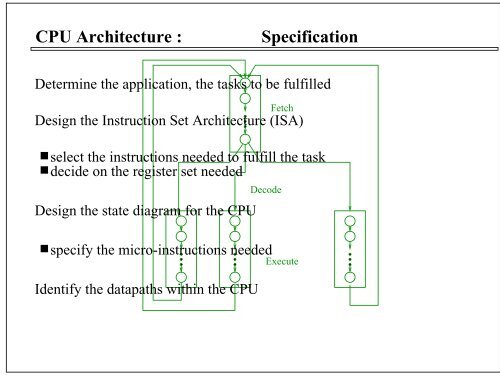
<strong>CPU</strong> Architecture : Specification<br />
Determine the application, the tasks to be fulfilled<br />
Fetch<br />
<strong>Design</strong> the Instruction Set Architecture (ISA)<br />
select the instructions needed to fulfill the task<br />
decide on the register set needed<br />
<strong>Design</strong> the state diagram for the <strong>CPU</strong><br />
Decode<br />
specify the micro-instructions needed<br />
Identify the datapaths within the <strong>CPU</strong><br />
Execute
<strong>CPU</strong> Architecture : Carpinelli’s very simple <strong>CPU</strong>.<br />
It can access 64 words of memory. Each word is 8 bits wide.<br />
It outputs a 6 bit address on pins A[5 .. 0]<br />
D0<br />
and reads an 8 bit value on pins D[7 D1 .. 0]<br />
It has four instructions :<br />
ADD<br />
AND<br />
JMP<br />
INC<br />
D2<br />
D3<br />
D4<br />
D5<br />
D6<br />
D7<br />
Accumulator<br />
A0<br />
A1<br />
A2<br />
A3<br />
A4<br />
A5<br />
read<br />
It has one programmer accessible register :<br />
AC an 8-bit accumulator
<strong>CPU</strong> Architecture : Carpinelli’s very simple <strong>CPU</strong>.<br />
It will require the following register set<br />
8 bit Accumulator, AC<br />
6 bit Program Counter, PC<br />
6 bit Address Register, AR<br />
8 bit Data Register, DR<br />
2 bit Instruction Register, IR
<strong>CPU</strong> Architecture : Fetch - Execute.<br />
Instruction Op−code Operation<br />
ADD 00AAAAAA AC
<strong>CPU</strong> Architecture : Fetch cycle. 1<br />
The fetch phase will take three states :<br />
FETCH1: AR PC<br />
As AR will be connected to A[5..0], this places the address on the address<br />
pins<br />
FETCH2: DR M, PC PC + 1<br />
Assert ’read’, data available on D[7..0], store in DR. Increment the<br />
Program Counter.
<strong>CPU</strong> Architecture : Fetch - cycle. 2<br />
FETCH3: IR DR[7..6], AR DR[5..0]<br />
Copy the instruction into the IR.<br />
Copy the lower 6 bits into the AR as if it’s an<br />
ADD<br />
or an<br />
AND<br />
then this will be the address to get the data from.<br />
This saves one cycle during execute.
<strong>CPU</strong> Architecture : establish the execute steps.<br />
FETCH1<br />
ADD1: DR M<br />
ADD2: AC AC + DR<br />
FETCH2<br />
AND1: DR M<br />
AND2: AC AC ^ DR<br />
IR=00<br />
FETCH3<br />
IR=11<br />
JMP1: PC DR[5..0]<br />
ADD<br />
IR=01<br />
AND<br />
IR=10<br />
JMP<br />
INC<br />
INC1: AC AC + 1<br />
execute<br />
execute<br />
execute<br />
execute<br />
cycle<br />
cycle<br />
cycle<br />
cycle
<strong>CPU</strong> Architecture : Establish data paths.<br />
READ<br />
6<br />
M<br />
Sort the register<br />
transfers by destination<br />
6<br />
AR<br />
A[5..0]<br />
6<br />
6 6<br />
D[7..0]<br />
AR : AR PC<br />
AR DR[5..0]<br />
6<br />
PC<br />
6 6<br />
PC : PC PC + 1<br />
PC DR[5..0]<br />
8<br />
8<br />
DR<br />
AC<br />
8 8<br />
8 8<br />
AC : AC AC + DR<br />
AC AC ^ DR<br />
AC AC + 1<br />
2<br />
IR<br />
2<br />
2<br />
IR : IR DR[7..6]<br />
CLK<br />
8 bit bus
<strong>CPU</strong> Architecture : Register Selection.<br />
AR only supplies data to memory, not other components<br />
IR doesn’t supply data to any component via the internal bus<br />
AC does not supply data to any component<br />
Bus is 8 bits wide, but not all registers are, so specify the width of<br />
connections<br />
AC must load sum of AC and DR, also logical AND of AC and DR so<br />
we need an ALU
<strong>CPU</strong> Architecture : Control Signals.<br />
We need a load signal for all registers that act as destinations for data<br />
We need bus enable signals for those registers that output data to the<br />
internal bus<br />
We need to ensure that all transfers that take place in the same state can<br />
occur simultaneously<br />
We need to be able to increment the PC register and the AC register.
<strong>CPU</strong> Architecture : Final Register Selection.<br />
READ<br />
M<br />
6<br />
A[5..0]<br />
D[7..0]<br />
6<br />
MEMBUS<br />
6<br />
LD<br />
AR<br />
ARLOAD<br />
PCBUS<br />
6 6<br />
6<br />
PC<br />
LD<br />
INC<br />
PCLOAD PCINC<br />
DRBUS<br />
8<br />
LD<br />
DR<br />
8 8<br />
DRLOAD<br />
8<br />
8<br />
LD<br />
ACLOAD<br />
AC<br />
INC<br />
ACINC<br />
2 [7..6]<br />
LD<br />
IRLOAD<br />
IR<br />
8 bit bus
<strong>CPU</strong> Architecture : Simple ALU.<br />
AC<br />
8<br />
8<br />
MUX<br />
DR<br />
8<br />
parallel<br />
adder<br />
8<br />
1<br />
0<br />
S<br />
8<br />
to AC<br />
control signal
<strong>CPU</strong> Architecture : Hardwired Control.<br />
input<br />
Counter<br />
Decoder<br />
Logic<br />
control<br />
signals<br />
clk<br />
ld<br />
inc clr<br />
This <strong>CPU</strong> has 9 states therefore we need :<br />
a 4 bit counter<br />
a 4 to 16 decoder of which 7 outputs will not be used.
<strong>CPU</strong> Architecture : Assigning states.<br />
1) Assign FETCH1 to counter value 0 and use the CLR input to the<br />
counter to get input to this state.<br />
Counter<br />
clk<br />
it’s reached from four ld inc states.<br />
clr<br />
Decoder<br />
FETCH1 is the only state that can be reached by more than one state,<br />
Logic<br />
control<br />
signals<br />
Branches to FETCH1 can then be made by clearing the counter, this is<br />
easy to implement in the control unit logic.<br />
All the other states can only be reached from one other state.
<strong>CPU</strong> Architecture : Sequential States.<br />
2) Assign sequential states to sequential counter values, using the INC<br />
input to the counter input to traverse the states.<br />
ld<br />
Counter<br />
inc clr<br />
Decoder<br />
clk<br />
Again this reduces the required control logic as a state need only assert<br />
the INC signal.<br />
Logic<br />
control<br />
signals<br />
eg. Assign counter value 1 to FETCH2 and counter value 2 to FETCH3.<br />
Similarly AND1 and AND2 would be assigned consecutive values.
<strong>CPU</strong> Architecture : Execute States.<br />
3) Use the instruction opcode to assign the first state of each execute<br />
routine, allowing for the maximum number of steps required for an<br />
execute routine.<br />
input<br />
Counter<br />
Decoder<br />
eg. if the longest execute cycle is 4 steps and assuming an opcode ’01’<br />
Logic<br />
control<br />
signals<br />
clk<br />
then a state value of ld inc ’0100’ clr would be suitable for the first step.<br />
Use the opcode as data input to the counter and load (ld) this value into<br />
the counter as the start point for the execute cycle<br />
load 0100 ->inc, 0101 -> inc, 0110 -> inc, 0111 ->clr, 0000
<strong>CPU</strong> Architecture : States attempt 1<br />
The input to the counter needs to be a function of IR<br />
The function needs to be as simple as possible<br />
1 0 IR[1..0]<br />
This gives load values of<br />
IR Counter value State<br />
00 1000 ADD1<br />
01 1001 AND1<br />
10 1010 JMP1<br />
11 1011 INC1
<strong>CPU</strong> Architecture : States attempt 2<br />
Given that there are a maximum of two states for an execute<br />
1 IR[1..0] 0 gives a better mapping<br />
IR Counter value State<br />
00 1000 ADD1<br />
1001 ADD2<br />
01 1010 AND1<br />
1011 AND2<br />
10 1100 JMP1<br />
11 1110 INC1
<strong>CPU</strong> Architecture : Control Signals<br />
1 IR[1..0]0<br />
4<br />
Counter<br />
LD INC CLR<br />
4<br />
Decoder<br />
0<br />
1<br />
2<br />
.<br />
.<br />
.<br />
8<br />
9<br />
10<br />
11<br />
12<br />
.<br />
.<br />
.<br />
14<br />
.<br />
FETCH1<br />
FETCH2<br />
FETCH3<br />
ADD1<br />
ADD2<br />
AND1<br />
AND2<br />
JMP1<br />
INC1<br />
ADD2<br />
AND2<br />
JMP1<br />
INC1<br />
FETCH1<br />
FETCH2<br />
ADD1<br />
AND1
<strong>CPU</strong> Architecture : Control Signals 2<br />
PCLOAD = JMP1<br />
PCINC = FETCH2<br />
DRLOAD = FETCH2 \/ ADD1 \/ AND1<br />
ACLOAD = ADD2 \/ AND2<br />
ACINC = INC1<br />
IRLOAD = FETCH3<br />
MEMBUS = FETCH2 \/ ADD1 \/ AND1<br />
PCBUS = FETCH1<br />
READ = FETCH2 \/ ADD1 \/ AND1
<strong>CPU</strong> Architecture : States attempt 1<br />
FETCH1<br />
FETCH3<br />
ARLOAD<br />
FETCH3<br />
IRLOAD<br />
AND2<br />
ALUSEL<br />
JMP1<br />
FETCH2<br />
PCLOAD<br />
PCINC<br />
FETCH2<br />
ADD1<br />
AND1<br />
MEMBUS<br />
FETCH2<br />
ADD1<br />
AND1<br />
DRLOAD<br />
FETCH1<br />
PCBUS<br />
ADD2<br />
AND2<br />
ACLOAD<br />
FETCH3<br />
ADD2<br />
AND2<br />
JMP1<br />
DRBUS<br />
INC1<br />
ACINC<br />
FETCH2<br />
ADD1<br />
AND1<br />
READ